JP2004363500A - Nitride-based compound semiconductor and method for manufacturing the same - Google Patents
Nitride-based compound semiconductor and method for manufacturing the same Download PDFInfo
- Publication number
- JP2004363500A JP2004363500A JP2003162914A JP2003162914A JP2004363500A JP 2004363500 A JP2004363500 A JP 2004363500A JP 2003162914 A JP2003162914 A JP 2003162914A JP 2003162914 A JP2003162914 A JP 2003162914A JP 2004363500 A JP2004363500 A JP 2004363500A
- Authority
- JP
- Japan
- Prior art keywords
- nitride
- compound semiconductor
- based compound
- layer
- semiconductor layer
- Prior art date
- Legal status (The legal status is an assumption and is not a legal conclusion. Google has not performed a legal analysis and makes no representation as to the accuracy of the status listed.)
- Pending
Links
Images


Abstract
Description
【0001】
【発明の属する技術分野】
本発明は、III−V族窒化物系化合物半導体を用いた発光ダイオードや半導体レーザなどの発光デバイス用あるいは高出力電界効果トランジスタ等の電子デバイス用の低転位窒化物系化合物半導体結晶に関する。
【0002】
【従来の技術】
窒化物系化合物半導体は、発光スペクトルが紫外から赤色の広範囲に渡る直接遷移型の半導体であり、発光ダイオード(LED)やレーザダイオード(LD)等の発光素子に応用されている。窒化物系化合物半導体結晶のエピタキシャル成長は、格子整合する基板の入手が困難なため、一般にサファイアやSiC基板上にバッファ層を介してエピタキシャル成長している。この場合、エピタキシャル膜と基板の格子不整合のため、成長界面から欠陥が導入され、エピタキシャル膜表面には108〜1010cm−2の転位が存在する。このためLEDやLD等の発光素子の信頼性において悪影響を与えることになるので、様々な転位密度を減らす方法が試みられている。
【0003】
転位密度を減らす方法の代表的な例として、エピタキシャル・ラテラル・オーバーグロース(ELO)という選択成長を用いた方法がある。この方法は、SiO2などのマスク材料を用いて窒化物系化合物半導体の表面にパターニングを施与して選択成長を行い、このマスク材料を埋め込むまで成長して、マスク材料により転位が遮断されて転位密度の低減がなされるものである。しかし、マスク材料を用いて窒化物系化合物半導体の表面に所定のマスクパターンを形成するには、フォトリソグラフィーやエッチングなど多くのプロセスを必要とし、また、マスクの開口部においては、転位は低減されないので、部分的に高密度の転位が残留してしまうという欠点もある。
【0004】
これに対して、マスク材料を用いることなしに炉内プロセスのみで転位密度を減らす方法の一つとして、以下に示す方法が田中らにより報告されている。
【0005】
図21に示すように、この方法は、基板1上に、窒化物系化合物半導体からなる低温堆積緩衝層2、高転位(転位密度>108cm−2)な第一の窒化物系化合物半導体層3を成長させる。但し、第一の窒化物系化合物半導体層3は、低温堆積緩衝層2を含むものとする。
【0006】
次に、一時成長を中断してアンモニアの供給を止め、欠陥抑制物質であるシリコンの原料のテトラエチルシランを供給する。これにより、第一の窒化物系化合物半導体層3の表面に薄いシリコン層4が形成される。この上に、さらに第二の窒化物系化合物半導体層5を成長させると、転位6の密度(転位密度)が大幅に減少し、107cm−2台以下の低転位な窒化物系化合物半導体ウエハを得ることができる(非特許文献1参照。)。
【0007】
この方法による転位低減の機構は未だ明らかではないが、以下の様に推察される。まず、第一の窒化物系化合物半導体層3上にシリコン層4を成長することで、第一の窒化物系化合物半導体層3の表面に存在する転位が終端される。その表面にシリコンを成長する場合、シリコンは窒素のダングリングボンド(未結合手)に優先的に取りこまれる。通常の窒化物系化合物半導体はIII族極性のC面を表面としているので、ステップ位置を除けば、窒素のダングリングボンドが存在するのは転位芯のみである。すなわち、通常の窒化物系化合物半導体上にシリコンを成長した場合、シリコンは転位が存在する部分に優先的に取りこまれ、転位の伝播が阻止されることが期待される。転位芯がシリコンにより終端される割合は、シリコンの供給量が多いほど高いので、転位密度を十分低減するためには、ある程度の量のシリコンを供給する必要がある。
【0008】
【非特許文献1】
Japanese Journal of Applied Physics vol.39(2000)pp.L831−L834
【0009】
【発明が解決しようとする課題】
しかし、従来の窒化物系化合物半導体の製造方法は、上記のようにマスク材料を用いることなしに転位密度を減らす方法であるが、第一の窒化物系化合物半導体層3が高温状態にさらされ、このため、表面からの窒素の脱離を抑制できず、シリコン層4の形成中に第一の窒化物系化合物半導体層3の表面が粗れてしまう。
【0010】
このような表面の粗れは、その上に成長した第二の窒化物系化合物半導体層5の中に新たな転位を発生する原因となり、シリコンの欠陥抑制物質としての効果が薄れてしまう。この結果、転位密度が高くなり(高転位となり)、窒化物系化合物半導体の品質が低下することになる。
【0011】
さらに、上記表面の粗れは、その上に成長する第二の窒化物系化合物半導体層5の表面にも引き継がれる。そのような粗れた表面上(ウエハ上)に、実際の窒化物系化合物半導体デバイスを形成すると、そのデバイスの特性が低下する。
【0012】
本発明は、かかる点に鑑みてなされたものであり、マスク材料を用いることなしに、表面が平坦で低転位な窒化物系化合物半導体層を形成可能とすることによって高品質な窒化物系化合物半導体を製造することができ、その平坦な表面上に形成される窒化物系化合物半導体デバイスの特性を向上させることができる窒化物系化合物半導体の製造方法および窒化物系化合物半導体を提供することを目的とする。
【0013】
【課題を解決するための手段】
上記課題を解決するために、本発明の窒化物系化合物半導体の製造方法は、基板上に成長した転位を含む第一の窒化物系化合物半導体層と、第一の窒化物系化合物半導体層よりも少ない転位を含む第二の窒化物系化合物半導体層との間に欠陥抑制物質層が存在する構成の窒化物系化合物半導体の製造方法において、前記欠陥抑制物質層がシリコン層である場合に、前記シリコン層形成時にシリコン原料を供給する際に同時にアンモニアを供給することを特徴としている。ここで、シリコン原料としては、テトラエチルシランが最適である。
【0014】
このように、テトラエチルシランとアンモニアを同時に供給することにより、第一の窒化物系化合物半導体層の表面からの窒素の脱離を抑制でき、新たな欠陥の導入と表面の粗れを防ぐことができる。そのシリコン層の上に第二の窒化物系化合物半導体層を成長させると、シリコンと窒化物系化合物半導体との間の格子不整合により、窒化物系化合物半導体は層状には成長せず、島状構造に成長し、さらに、窒化物系化合物半導体の成長を続けると、島同士が融合し、最終的には平坦な表面が得られる。
【0015】
また、基板は、Si、SiC、サファイア、GaN、AlNの何れかであることを特徴としている。
【0016】
このように、最上層が窒化物系化合物半導体層であれば基板の種類によらず適用可能なのは明らかである。
【0017】
また、前記第一の窒化物系化合物半導体層は、窒化物系化合物半導体単層膜および、異なる組成を有する複数の窒化物系化合物半導体単層から成る多層膜構造の何れかであることを特徴としている。
【0018】
このように、第一の窒化物系化合物半導体層の構成によらず適用可能である。すなわち、第一の窒化物系化合物半導体層は、任意組成の単層膜、異なる組成の窒化物半導体を組み合わせた多層膜のいずれでも良く、またドーピングについても制限は無い。
【0019】
また、前記第一の窒化物系化合物半導体層の膜厚は、10μm以下であることを特徴としている。
【0020】
このように、第一の窒化物系化合物半導体層の膜厚は、ウエハコストとウエハの反りの観点から、10μm以下とするのが望ましい。好ましくは1μm以下、より好ましくは0.3μm以下がよい。
【0021】
また、前記第一の窒化物系化合物半導体層の成長温度は、900℃以上、1200℃以下であることを特徴としている。
【0022】
このように、第一の窒化物系化合物半導体層は、900℃以上、1200℃以下の温度で窒化物半導体を成長してなる。この成長温度範囲外では、窒化物系化合物半導体層の表面は、高温により粗れたり、低温により3次元成長が促進されて表面起伏が大きくなる等の問題が生じる。上記の成長温度範囲では平坦な表面が得られ、その上に成長するシリコン層及び第二の窒化物系化合物半導体層も平坦な表面を得ることが可能となる。さらに第一の窒化物系化合物半導体層は、多層膜であってもよく、900℃より低温で窒化物半導体バッファ層を成長した上に上記の温度範囲で窒化物半導体を成長してなる層であってもよい。
【0023】
また、前記シリコン層を形成する際のテトラエチルシランの供給速度は、1μmo1/分以上、100μmo1/分以下であることを特徴としている。
【0024】
ここで、供給速度が100μmol/分を越えると、ウェハ面内に均一にシリコン層が形成されず、その上に成長する島状構造も不均一な分布となる。このため島状構造が粗な部分は島同士の間隔が大きいため埋まりにくくなり、表面に窪みが残留する。また、供給速度が1μmol/分より遅くなると、シリコン層形成時に第一の窒化物系化合物半導体層の表面が長時間高温にさらされることになり、表面が粗れてしまう。従って、テトラエチルシランの供給速度範囲が最適であり、より好ましくは10μmol/分以上、50μmol/分以下とするのがよい。
【0025】
また、前記シリコン層を形成する際のテトラエチルシランの供給量は、0.1μmol以上、50μmol以下であることを特徴としている。
【0026】
このようなシリコンの供給量により、その上に選択的に成長する窒化物系化合物半導体の島状構造の島密度が変化する。シリコンの供給量が50μmolを越えると島密度が極端に低くなり、第二の窒化物系化合物半導体層の平坦化が困難で、表面に窪みが残留する。シリコンの供給量が0.1μmolより少なくなるとシリコン層が殆ど形成されなくなり、下地の転位がそのまま上の層にも伝播し、転位密度が高くなる。従って、テトラエチルシランの供給量の範囲にすることで表面が平坦かつ低転位な窒化物半導体層を形成できる。より好ましくは1μmol以上、10μmol以下とするのがよい。
【0027】
また、前記シリコン層を形成する際の成長装置内のアンモニア濃度は、0.1%以上、50%以下であることを特徴としている。
【0028】
このように、窒化物系化合物半導体表面からの窒素の脱離による新たな欠陥の発生を抑制し、表面が粗れないようにするためには、アンモニア濃度を0.1%以上、より好ましくは1%以上とするのがよい。アンモニアとテトラエチルシランの気相反応による表面に到達するシリコン量の低下を抑制するためには、アンモニア濃度を50%以下、より好ましくは、25%以下とするのがよく、上記アンモニア濃度範囲で、平坦かつ低転位な窒化物半導体が得られる。
【0029】
また、前記第一の窒化物系化合物半導体層の形成終了後に、前記シリコン層の形成を開始するまでの時間が10秒以下であることを特徴としている。
【0030】
この場合、窒化物系化合物半導体を成長せずに10秒以上高温にさらすと表面が粗れるため、短い方がよい。また、シリコン層の形成終了後に第二の窒化物系化合物半導体層の形成を開始するまでの時間も同様な理由で10秒以下とするのがよい。
【0031】
さらに、前記シリコン層の厚さは、0.1原子層〜1nmとするのがよい。シリコン層の厚さが、0.1原子層未満では十分な欠陥抑制効果が得られず、また、1nmより厚い場合には第一の窒化物系化合物半導体層とシリコン層の間の格子不整合の影響が大きくなり、界面に新たな転位を導入してしまうからである。
【0032】
また、前記シリコン層の成長時の基板温度は、前記第一の窒化物系化合物半導体層を形成する際の基板温度±100℃以内であることを特徴としている。
【0033】
この理由を述べる。第一の窒化物系化合物半導体層形成後、シリコン層を形成しながら成長温度を変えると、テトラエチルシランの分解効率が温度変化に伴い変化するので、ウエハ表面に到達するシリコンの量が変化してしまい、一定量を供給できなくなる。このため、第一の窒化物系化合物半導体層形成後、温度を変えてからシリコン層を形成することになるが、温度差が100℃以上あると、シリコン層を形成する前に温度を一定に保つまでかなりの時間がかかり、第一の窒化物半導体層表面が粗れてしまう。従って、上記温度範囲内とするのがよく、より好ましくは±50℃以内とするのがよい。
【0034】
また、前記第二の窒化物系化合物半導体層を形成する工程は、前記シリコン層の上に窒化物系化合物半導体を成長して窒化物系化合物半導体による島状構造を形成する第1の工程と、前記島状構造をさらなる窒化物系化合物半導体の成長により平坦化する第2の工程とから成ることを特徴としている。
【0035】
さらに、前記島状構造を形成する際の原料供給レートが、窒化物系化合物半導体が層状に成長した場合の窒化物系化合物半導体の成長速度として0.1nm/s以上でかつ10nm/s以下となる原料供給レートに対応させるのがよい。この場合、島状構造形成時の原料供給レートにより、島密度が変化する。島状構造が、層状に成長した場合に0.1nm/sより遅い成長速度に対応する原料供給レートで成長すると、島密度が低過ぎて第二の窒化物系化合物半導体層の平坦化は困難となり、表面に窪みが残留する。また、前記島状構造が、層状に成長した場合に10nm/sより速い成長速度に対応する原料供給レートで成長すると、島密度が非常に高くなり、島同士の融合時に発生しやすい転位の数も増え、転位密度が高くなってしまう。従って、上記の原料供給レートとすることで、表面を完全に平坦化し、かつ低転位な窒化物半導体層を形成できる。より好ましくは0.5nm/s以上でかつ5nm/s以下とするのがよい。
【0036】
また、前記島状構造を形成する際の原料供給量は、窒化物系化合物半導体が層状に成長した場合の窒化物系化合物半導体の膜厚が、1〜1000nmとなる原料供給量に対応することを特徴としている。
【0037】
ここで、島状構造が、層状に成長した場合に1nmより薄い膜厚に対応する原料供給量で成長すると、島状構造が十分に形成されていないため、格子不整合を緩和できず、新たな転位を発生する原因となる。島状構造が、層状に成長した場合に1000nmより厚い膜厚に対応する原料供給量で成長すると、島が高くなり過ぎて埋め込み平坦化が困難となり、表面に窪みが残留してしまう。従って、膜厚1〜1000nmに対応する原料供給量とすることで、表面を完全に平坦化し、かつ低転位な窒化物半導体層を形成できる。より好ましくは5〜100nmとするのがよい。
【0038】
また、前記島状構造の密度は、103〜109cm−2であることを特徴としている。
【0039】
島状構造の密度は、シリコン層形成時のテトラエチルシランの供給量と島状構造形成時の原料供給レートで制御できる。島密度が103cm−2より低いと平均的な島同士の間隔が数百μmにもわたり、これを埋め込み平坦化するには、通常その間隔と同じくらいの膜厚を成長しなければならず、平坦化が非常に困難となる。また、島密度が多すぎるとほとんど平坦成長時と同じ状態になり、転位低減されなくなる。従って、島密度を103〜109cm−2とすることで、平坦な表面かつ低転位な窒化物半導体層を形成できる。より好ましくは106〜108cm−2とするのがよい。
【0040】
また、前記島状構造を形成する際の基板温度は、前記シリコン層形成時の基板温度±100℃以内であることを特徴としている。
【0041】
シリコン層形成後、島状構造を形成しながら成長温度を変えると、原料の分解効率が温度変化に伴い変化するので、原料供給レートが時間と共に変化し、島の密度を制御できなくなる。このため、シリコン層形成後、温度を変えてから島状構造を形成することになるが、温度差が100℃以上あると、島状構造を形成する前に温度を一定に保つまでかなりの時間がかかり、成長中表面が粗れてしまう。従って、上記温度範囲内とするのがよい。
【0042】
また、前記第2の工程における窒化物系化合物半導体の成長条件は、少なくとも次の(a)〜(e)の何れか1つの要件を満たすように設定されることを特徴としている。(a)基板温度を前記島状構造の形成時よりも高くする。このように、高温にすることで横方向成長が促進され、より薄く埋め込み平坦化が可能となる。(b)成長速度を前記島状構造の形成時よりも速くする。このように、成長速度が大きければ、より速く平坦化が可能である。(c)V族/III族の原料のモル比を前記島状構造の形成時よりも低くする。これにより窒化物系化合物半導体の横方向成長が促進され、より薄く埋め込み平坦化が可能となる。(d)成長装置内の雰囲気ガスに占める水素の割合を前記島状構造の形成時よりも低くする。これにより窒化物系化合物半導体層の横方向成長を促進し、表面をより速く平坦化できる。(e)成長圧力を前記島状構造の形成時よりも低くする。これにより窒化物系化合物半導体の横方向成長が促進され、より薄く埋め込み平坦化が可能となる。
【0043】
また、前記第2の工程における基板温度は、前記第1の工程における基板温度よりも10℃以上、200℃以下の範囲で高いことを特徴としている。
【0044】
これによって、埋め込み平坦化過程における基板温度をシリコン層形成時および、島状構造形成時の基板温度よりも高くする事で横方向成長が促進され、より薄く埋め込み平坦化できる。ただし、10℃以下では殆ど効果がなく、200℃以上高くすると、表面が粗れるため、上記温度範囲内で高くするのがよい。より好ましくは20℃以上70℃以下の範囲内で高温とするのがよい。
【0045】
また、前記第二の窒化物系化合物半導体層の膜厚は、100μm以上であることを特徴としている。
【0046】
このように、膜厚が100μm以上あれば基板を剥がして、低転位な自立した窒化物系化合物半導体基板を形成することができる。さらに、第二の窒化物系化合物半導体層の膜厚は、本発明における島状構造の平坦化の観点からいうと100μm以下の膜厚で十分である。ウエハコストとウエハの反りの観点から、5μm以下が望ましく、より好ましくは2μm以下がよい。
【0047】
また、前記第一の窒化物系化合物半導体層、前記シリコン層および前記第二の窒化物系化合物半導体層を形成する際の成長圧力は、10〜760Torr(約13.3〜約1013.2hPa)の範囲内であることを特徴としている。
【0048】
ここで、成長圧力が10Torr(約13.3hPa)より低いと、原料の分圧が低すぎて、窒化物系化合物半導体層表面から窒素の脱離が激しくなり、欠陥が多くなってしまう。逆に圧力が760Torr(約1013.2hPa)よりも高くなると、窒化物系化合物半導体層の横方向成長が遅く、表面を埋め込み平坦化するのが難しくなる。このため上記の成長圧力範囲が望ましく、より好ましくは75〜350Torr(約100.0〜約466.6hPa)がよい。
【0049】
また、前記第一の窒化物系化合物半導体層および前記第二の窒化物系化合物半導体層を形成する際のIII族原料とV族原料のモル比は、1:100〜10000
であることを特徴としている。
【0050】
III族原料とV族原料の比が1:100より小さくなると窒化物の析出の駆動力が極端に減少するため成長しにくくなる。また、10000以上にする場合、III族原料の分圧を低くすると、エッチングされやすく、成長しにくい。従って、上記のIII族原料に対するV族原料の比の範囲内とするのがよく、好ましくは1:1000〜3000とするのがよい。
【0051】
さらに、本発明における成長の方法は、窒化物系化合物半導体を成長できればよく、MOVPE、MBEあるいはHVPEであってもよい。さらに上記発明により作製された低転位窒化物系化合物半導体上に形成された窒化物系化合物半導体デバイスは、転位の減少により、光デバイスにおいては非発光中心が少なくなり発光輝度が向上し、電子デバイスにおいては散乱中心が少なくなって移動度を向上させることができる。
【0052】
また、本発明の窒化物系化合物半導体は、基板上に成長した転位を含む第一の窒化物系化合物半導体層と、第一の窒化物系化合物半導体層よりも少ない転位を含む第二の窒化物系化合物半導体層との間に欠陥抑制物質層を介在して構成される窒化物系化合物半導体において、前記欠陥抑制物質層は、シリコン原料と、アンモニアとが同時に供給されて形成されたシリコン層であることを特徴としている。ここで、シリコン原料としては、テトラエチルシランが最適である。
【0053】
【発明の実施の形態】
以下、本発明の実施の形態について、図面を参照して詳細に説明する。
【0054】
(実施の形態)
図1(a)〜(e)に示す本実施の形態に係る窒化物系化合物半導体基材10は、基板1上に窒化物系化合物半導体からなる低温堆積緩衝層2、第一の窒化物系化合物半導体層3を成長させ、その後、成長を一時中断してシリコン原料であるテトラエチルシランとアンモニアを同時に供給して欠陥抑制物質層であるシリコン層4を形成し、その上に第二の窒化物系化合物半導体層5を成長させた構造となっている。但し、第一の窒化物系化合物半導体層3は、この層3と異なる組成を有する窒化物系化合物半導体による低温堆積緩衝層2を含む多層膜構造、または窒化物系化合物半導体単層膜(この場合、低温堆積緩衝層2は存在しない)であるとする。
【0055】
この窒化物系化合物半導体基材10(窒化物系化合物半導体)の製造方法の特徴は、上記テトラエチルシランとアンモニアを同時に供給する点にある。
【0056】
つまり、基板1上に成長した転位を多く含む第一の窒化物系化合物半導体層3を含む複合基板と、転位の少ない第二の窒化物系化合物半導体層5との間に欠陥抑制物質であるシリコン層4が存在する構造において、シリコン層4の形成時にシリコン原料であるテトラエチルシランとアンモニアを同時に供給することにより、第一の窒化物系化合物半導体層3の表面からの窒素の脱離を抑制でき、新たな欠陥の導入と表面の粗れを防ぐことができる。これによって、表面が平坦かつ低転位な窒化物系化合物半導体層を形成することが可能となる。
【0057】
ここで、転位が低減された際に観察された成長過程について述べる。第一の窒化物系化合物半導体層3上にシリコン層4を成長させることにより、転位が終端されるのは前述の通りである。シリコン層4上に第二の窒化物系化合物半導体層5を成長させる際には、成長は以下の様に推移する。
【0058】
まず、成長初期においては、シリコン層4を形成するためのシリコンと、第二の窒化物系化合物半導体層5を形成するための第二の窒化物系化合物半導体との間の格子不整合により、第二の窒化物系化合物半導体は層状には成長せず、図1(c)に示すように、島状構造5aに成長する。更に、第二の窒化物系化合物半導体の成長を続けると、島同士が融合し、最終的には平坦な表面が得られる。即ち、図1(d)に示すように、島状構造平坦化層5bが得られる。
【0059】
但し、成長条件によっては、シリコン層4上の第二の窒化物系化合物半導体層5を成長初期から層状に成長することも可能である。しかし、その場合には、シリコンと窒化物系化合物半導体との間の格子不整合に起因する新たな転位が発生し、十分な転位低減が達成できない。
【0060】
そこで、第二の窒化物系化合物半導体層5の成長初期を島状成長とすることで、上述の格子不整合を緩和し、新たな転位の発生を抑制することが出来る。さらに言えば、第二の窒化物系化合物半導体層5の成長初期には島状成長を促進する条件を積極的・意図的に選ぶ必要がある。上述の手法においては、基板1、第一の窒化物系化合物半導体層3、シリコン層4、第二の窒化物系化合物半導体層5という多くの構成要素が存在する。このため、それぞれの構成要素の詳細、および、構成要素の成長条件などにより、転位の低減効果が影響されることが予想される。すなわち、シリコンの欠陥抑制物質としての働きを十分に引き出すために必要な要件を規定すれば、より良い効果を得ることができる。以下、その必要な要件を加味して実際に行った窒化物系化合物半導体の製造方法の実施例を説明する。
(実施例1)
本実施例1は、転位を多く含む第一の窒化物系化合物半導体層3の上に、シリコン原料であるテトラエチルシランと、アンモニア濃度とを変化させて同時に供給し、欠陥抑割物質層であるシリコン層4を形成した。さらに、その上に第二の窒化物系化合物半導体層5を形成し、最表層での転位密度を減少させるようにしたものである。
【0061】
まず、上記基板1としてサファイア基板を用い、これを、有機金属気相成長(以下、MOVPEと略す)装置にセットし、水素窒素混合ガス雰囲気下で1200℃まで昇温させ、サーマルクリーニングを行った。その後、温度を500℃まで下げ、成長圧力300Torr(約400.0hPa)とし、ガリウム原料としてトリメチルガリウム(以下、TMGと略す)、窒素原料としてアンモニアを流し、低温堆積緩衝層2としてGaN低温堆積緩衝層を30nm成長させた。
【0062】
次に、成長温度を1000℃に昇温させ、TMGおよびアンモニアを流し、第一の窒化物系化合物半導体層3としてGaN層を2μm成長させた。
【0063】
その後、同じ成長温度、圧力を保持したまま、TMGの供給を止めて成長を5秒間中断した。その間、成長装置内のアンモニア濃度を0.05〜80%にして、シリコンの原料としてテトラエチルシランを供給速度30μmol/分で5μmol供給し、欠陥抑制物質層であるシリコン層4を形成した。
【0064】
その後、テトラエチルシランの供給を止め5秒間保持した後、平坦な表面上にGaN層を成長した場合に1nm/sの成長速度で成長する場合に対応するTMG供給レートで、再び第二の窒化物系化合物半導体層5としてGaN層を、20秒間成長させたところ、島状構造5aとしてのGaN島状構造が形成された。
【0065】
その後、温度をさらに50℃上げて1050℃とし、成長速度1nm/s、V族原料とIII族原料との比を1500とし、島状構造平坦化層5bとしてGaN層を4μm成長させたところ、表面が平坦化した。
【0066】
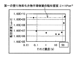
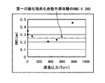
図2に、本実施例1で得られた窒化物系化合物半導体基材10の第二の窒化物系化合物半導体層5の転位密度とシリコン層4の形成時のアンモニア濃度との関係、並びに第一の窒化物系化合物半導体層3の転位密度を示す。
【0067】
図3に、本実施例1で得られた窒化物系化合物半導体基材10の第二の窒化物系化合物半導体層5の表面の粗さ{RMS(二乗平均平方根)値で表す粗さ}とシリコン層4の形成時のアンモニア濃度との関係、並びに第一の窒化物系化合物半導体層3の表面粗さ(RMS)を示す。
【0068】
この結果から、アンモニア濃度が0.1%以下と50%以上で転位密度が極端に増加し、表面も粗くなることが分かる。アンモニア濃度が1〜25%の範囲で最も転位密度が低くなり、最も低い値では2×106cm−2となった。すなわち従来の手法であるシリコン層4の形成時にアンモニアを供給しない場合よりも、転位密度を1桁以上低減することができた。また、第二の窒化物系化合物半導体層5であるGaN層の表面粗さもアンモニア濃度が1〜50%の範囲で小さくなっているのが分かる。
(実施例2)
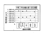
本実施例2は、上記実施例1において、シリコン層4の形成時のアンモニア濃度を20%とし、基板1をサファイア基板の代わりに、SiC、Si、AlN、GaN基板を用いて成長を行ったものである。
【0069】
SiCあるいはSi基板上に成長させる場合は、アルミニウム原料としてトリメチルアルミニウム(TMA)、窒素原料してアンモニアを用い、AlN層を1000℃で100nm成長させ、その後、第一の窒化物系化合物半導体層3としてGaN層を成長させ、以下、実施例1と同様な成長プロセスを経て窒化物系化合物半導体基材10を作製した。
【0070】
また、AlN、GaN基板では、直接1000℃で第一の窒化物系化合物半導体層3としてGaN層を成長させ、以下、実施例1と同様な成長プロセスを経て窒化物系化合物半導体基材10を作製した。
【0071】
図4に、各基板毎の第一の窒化物系化合物半導体層(第一のGaN層)3の転位密度と、第二の窒化物系化合物半導体層(第二のGaN層)5の転位密度を示す。この結果から分かるように、実施例1でサファイア基板を用いたものと同等な転位低減効果が得られ、それぞれ最表層での転位密度が、第一の窒化物系化合物半導体層3と比べ2桁近く低減している。
(実施例3)
本実施例3は、上記実施例1において、シリコン層4の形成時のアンモニア濃度を20%とし、第一の窒化物系化合物半導体層3を、GaN層とその上にA10.2GaN0.8層を積層させた構造としたものである。これにより作製された窒化物系化合物半導体基材10の最表層での転位密度は、2×106cm−2となり、第一の窒化物系化合物半導体層3の転位密度である2×109cm−2と比べ、2ケタ以上低減することができた。
【0072】
なお、窒化物系化合物半導体基材10の最表層とは、この例の場合、第二の窒化物系化合物半導体層5であり、以降、同様に表現する。
(実施例4)
本実施例4は、上記実施例1において、シリコン層4の形成時のアンモニア濃度を20%とし、第一の窒化物系化合物半導体層3の膜厚を、0.3〜15μmとしたものである。
【0073】
図5に、本実施例4で得られた窒化物系化合物半導体基材10の最表層での転位密度と第一の窒化物系化合物半導体層3の膜厚との関係、並びに第一の窒化物系化合物半導体層3の転位密度を示す。
【0074】
図6に、本実施例4で得られた窒化物系化合物半導体基材10の最表層での表面粗さ(RMS)と第一の窒化物系化合物半導体層3の膜厚との関係、並びに第一の窒化物系化合物半導体層3の表面粗さ(RMS)を示す。
【0075】
この結果から分かるように、最表層での転位密度は、第一の窒化物系化合物半導体層3の膜厚が大きくなるにつれてわずかに減少するが、10μm以上になると殆ど変化は見られなかった。また、第一の窒化物系化合物半導体層3の膜厚を0.3〜15μmに変化させてもRMS値に大きな変化は見られなかった。
(実施例5)
本実施例5は、上記実施例1において、シリコン層4の形成時のアンモニア濃度を20%とし、第一の窒化物系化合物半導体層3の形成時の成長温度を800℃〜1300℃としたものである。
【0076】
図7に、本実施例5で得られた窒化物系化合物半導体基材10の最表層の表面粗さ(RMS)と第一の窒化物系化合物半導体層3の形成時の成長温度との関係、並びに第一の窒化物系化合物半導体層3の表面粗さ(RMS)を示す。この結果から分かるように、成長温度が900℃以下と1200℃以上で表面粗さが極端に増加しているのが分かる。逆に、900℃以上1200℃以下では表面粗さが減少している。
(実施例6)
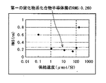
本実施例6は、上記実施例1において、シリコン層4の形成時のアンモニア濃度を20%とし、シリコン層4を形成する際のシリコン原料であるテトラエチルシランの供給速度を、0μmol/分〜150μmol/分まで変化させたものである。
【0077】
図8に、本実施例6で得られた窒化物系化合物半導体基材10の最表層の表面粗さ(RMS)とテトラエチルシランの供給速度との関係、並びに第一の窒化物系化合物半導体層3の表面粗さ(RMS)を示す。この結果から、供給速度が1μmol/分以下と100μmol/分以上で表面粗さが極端に増加しているのが分かる。逆に、1μmol/分以上100μmol/分以下で表面粗さが減少しているのが分かる。
(実施例7)
本実施例7は上記実施例1において、シリコン層4の形成時のアンモニア濃度を20%とし、シリコン層4を形成する際のシリコン原料であるテトラエチルシランの供給量を、0.05μmol〜80μmolまで変化させたものである。
【0078】
図9に、本実施例7で得られた窒化物系化合物半導体基材10の最表層の転位密度とテトラエチルシランの供給速度との関係、並びに第一の窒化物系化合物半導体層3の転位密度を示す。この結果から分かるように、本実施例7で作製された窒化物系化合物半導体基材10においては、テトラエチルシランの供給量が50μmolを越えると平坦化されず、最表層に窪みが残留した。また、0.1μmolより少なくなると転位密度が極端に高くなった。
(実施例8)
本実施例8は、上記実施例1において、シリコン層4の形成時のアンモニア濃度を20%とし、第一の窒化物系化合物半導体層3の形成終了後に、シリコン層4の形成を開始するまでの時間を、0〜20秒まで変化させたものである。
【0079】
図10に、本実施例8で得られた窒化物系化合物半導体基材10の最表層の表面粗さ(RMS)と、第一の窒化物系化合物半導体層3の形成終了後にシリコン層4の形成を開始するまでの時間との関係、並びに第一の窒化物系化合物半導体層3の表面粗さ(RMS)を示す。この結果から分かるように、10秒以下では、RMS値は低い値を保っているが10秒を越えると表面が粗れてしまい、RMS値が極端に増加した。
(実施例9)
本実施例9は、上記実施例1において、シリコン層4の形成時のアンモニア濃度を20%とし、第一の窒化物系化合物半導体層3の形成終了後に、成長温度を1000℃から、850℃〜1150℃までの上下に変化させ、実施例1と同様な成長プロセスにより、シリコン層4を形成し、窒化物系化合物半導体基材10を作製した。
【0080】
図11に、本実施例9で得られた窒化物系化合物半導体基材10の最表層の表面粗さ(RMS)と、第一の窒化物系化合物半導体層3の形成時の成長温度とシリコン層4の形成時の成長温度の差との関係、並びに第一の窒化物系化合物半導体層3の表面粗さ(RMS)を示す。この結果から分かるように、成長温度差が±100℃以上になると表面が粗れてしまい、RMS値が極端に増加した。逆に、成長温度差が±100℃以内では表面が平坦で、RMS値が減少している。
(実施例10)
本実施例10は上記実施例1において、シリコン層4の形成時のアンモニア濃度を20%とし、GaN島状構造5aを形成する際、窒化物系化合物半導体を層状に成長した場合の成長速度として、0.05nm/s〜15nm/sとなる場合に対応するTMG供給レートで成長したものである。
【0081】
図12に、本実施例10で得られた窒化物系化合物半導体基材10の最表層の転位密度と、平坦な表面上に窒化物系化合物半導体を成長した場合の成長速度で表されるGaN島状構造5aの形成時の成長速度との関係、並びに第一の窒化物系化合物半導体層3の転位密度を示す。この結果から、成長速度が0.05nm/sより遅い時は、島状構造5aを完全に平坦化できず、窪みが残留した。また、成長速度が10nm/sより速くなると、最初から殆ど平坦に成長してしまい、転位密度が極端に増加した。成長速度が0.1nm/s以上10nm/s以下で転位密度が減少している。
(実施例11)
本実施例11は上記実施例1において、シリコン層4の形成時のアンモニア濃度を20%とし、GaN島状構造5aを形成する際、窒化物系化合物半導体を層状に成長した場合の膜厚が、0.5nm〜1500nmとなるTMG供給量で成長したものである。
【0082】
図13に、本実施例11で得られた窒化物系化合物半導体基材10の最表層の表面粗さ(RMS)と、GaN島状構造5aにおいて窒化物半導体を層状に成長した場合の膜厚との関係、並びに第一の窒化物系化合物半導体層3の表面粗さ(RMS)を示す。この結果から、膜厚が1nmより小さい時と1000nmより大きくなる時、表面に窪みが残留し、RMS値は極端に増加した。膜厚が1nm以上1000nm以下で、RMS値が減少している。
(実施例12)
本実施例12は上記実施例1において、シリコン層4の形成時のアンモニア濃度を20%とし、GaN島状構造5aを形成する際、島密度が103〜109cm−2に対応するシリコン層4の形成時のテトラエチルシラン供給量と、島状構造5aの形成時のTMG供給レートで成長したものである。
【0083】
図14に、本実施例12で得られた窒化物系化合物半導体基材10の最表層の転位密度とGaN島状構造5aの密度との関係、並びに、第一の窒化物系化合物半導体層3の転位密度を示す。
【0084】
図15に、本実施例12で得られた窒化物系化合物半導体基材10の最表層の表面粗さ(RMS)とGaN島状構造5aの密度との関係、並びに第一の窒化物系化合物半導体層3の表面粗さ(RMS)を示す。
【0085】
この結果から、島密度が高くなるにつれて転位密度が高くなっており、島密度が109cm−2を越えると転位密度は109cm−2台となり、第一の窒化物系化合物半導体層3の転位密度と比べ、殆ど減少していないことが分かる。また、RMS値は、島密度が106〜108cm−2の時、最も低い値を示しており、それより島密度が低い時は、極端に高くなっていく傾向がある。さらに、島密度が103cm−2より低くなると、島状構造5aを殆ど平坦化できず、最表層には島状の突起が残る。
(実施例13)
本実施例13は上記実施例1において、シリコン層4の形成時のアンモニア濃度を20%とし、シリコン層4の形成終了後に、成長温度を1000℃から、850℃〜1150℃までの上下に変化させ、実施例1と同様な成長プロセスにより、GaN島状構造5aを形成し、窒化物系化合物半導体基材10を作製した。
【0086】
図16に、本実施例13で得られた窒化物系化合物半導体基材10の最表層の表面粗さ(RMS)と、シリコン層4の形成時の成長温度とGaN島状構造5aの形成時の成長温度の差との関係、並びに第一の窒化物系化合物半導体層3の表面粗さ(RMS)を示す。この結果から分かるように、成長温度差が100℃以上になると表面が粗れてしまい、RMS値が極端に増加した。100℃以内ではRMS値は小さい。
(実施例14)
本実施例14は上記実施例1において、シリコン層4の形成時のアンモニア濃度を20%とし、GaN島状構造5aの形成後、基板1の温度を1000℃よりも最高で250℃高い範囲まで変化させ、実施例1と同様な成長プロセスにより、島状構造平坦化層5bを形成した。
【0087】
図17に、本実施例14で得られた窒化物系化合物半導体基材10の最表層の表面粗さ(RMS)と、GaN島状構造形成時と平坦化層形成時の成長温度の差との関係、並びに第一の窒化物系化合物半導体層3の表面粗さ(RMS)を示す。この結果から分かるように、基板温度差が150℃を越えるようになると、表面が一部、若干粗れ始め、基板温度が1200℃、すなわちGaN島状構造5aの形成時より200℃以上高温になると、表面が全体的に粗れてしまった。
(実施例15)
本実施例15は上記実施例1において、シリコン層4の形成時のアンモニア濃度を20%とし、第二の窒化物系化合物半導体層5の膜厚を、2〜100μmとしたものである。本実施例15で得られた窒化物系化合物半導体基材10は全ての試料で表面は平坦化しており、転位密度は106cm−2となり、第一の窒化物系化合物半導体層3の転位密度である2×109cm−2と比べ、2ケタ以上低減することができた。
(実施例16)
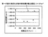
本実施例16は上記実施例1において、シリコン層4の形成時のアンモニア濃度を20%とし、成長圧力を5〜770Torr(約6.7〜約1026.6hPa)まで変化させたものである。
【0088】
図18に、本実施例16で得られた窒化物系化合物半導体基材10の最表層の転位密度と成長圧力との関係、並びに第一の窒化物系化合物半導体層3の転位密度を示す。
【0089】
図19に、本実施例16で得られた窒化物系化合物半導体基材10の最表層の表面粗さ(RMS)と成長圧力との関係、並びに第一の窒化物系化合物半導体層3の表面粗さ(RMS)を示す。これらの結果から、成長圧力が10Torr(約13.3hPa)以下では転位密度が非常に高くなり、また、成長圧力が760Torr(約1013.2hPa)以上ではRMS値が大きくなることが分かる。つまり、成長圧力が10Torr(約13.3hPa)を越えていれば転位密度を低く、また、成長圧力が760Torr(約1013.2hPa)よりも小さければRMS値を小さく押さえられることが分かる。
(実施例17)
本実施例17は上記実施例1において、シリコン層4の形成時のアンモニア濃度を20%とし、第一の窒化物系化合物半導体層3および第二の窒化物系化合物半導体層5を形成する際のIII族とV族原料の比を、1:50〜20000まで変化させたものである。
【0090】
図20に、本実施例17で得られた窒化物系化合物半導体基材10の最表層の表面粗さ(RMS)と、III族原料とV族原料の比との関係、並びに第一の窒化物系化合物半導体層3の表面粗さ(RMS)を示す。この結果から分かるように、III族原料とV族原料の比が1:100より小さい時、及び10000より大きい時は、RMS値が増大し、つまり最表層は平坦化されず、窪みが残留していた。逆に、III族原料とV族原料の比が1:100より大きい時、及び10000より小さい時は、RMS値が減少し、つまり最表層は平坦化されていた。
(実施例18)
本実施例18は上記実施例1において、シリコン層4の形成時にアンモニアを供給しない従来の手法と、アンモニア濃度を20%として作製した窒化物系化合物半導体基材10の上に、発光デバイス構造を順次成長して紫外LED(波長38nm)を作製したものである。発光デバイス部は、従来および本実施例18のものとも全く同じ構造のSQW構造とした。これら従来および本実施例18の発光素子に対し、20mAを通電し、この時の各々の発光出力を比較した。この結果、従来のものは2.2mW、本実施例18のものは5.5mWと従来のものに比べ、2倍以上発光出力が向上した。
【0091】
つまり、本発明の窒化物系化合物半導体基材10の上に、LEDやLDなどの半導体発光素子や受光素子、電子デバイスを作製すれば、その特性を飛躍的に向上させることができる。
(実施例19)
本実施例19は上記実施例1において、第一の窒化物系化合物半導体層3を低温堆積緩衝層2のみとした場合である。これにより得られた窒化物系化合物半導体基材10の最表層での転位密度は、107cm−2台となり、低温堆積緩衝層2の転位密度の1010cm−2台に比べ、3桁低減することができた。
【0092】
【発明の効果】
以上説明したように、本発明によれば、基板上に成長した転位を含む第一の窒化物系化合物半導体層と、第一の窒化物系化合物半導体層よりも少ない転位を含む第二の窒化物系化合物半導体層との間に欠陥抑制物質層が存在する構成の窒化物系化合物半導体を製造する際に、欠陥抑制物質層がシリコン層である場合、そのシリコン層形成時においてシリコン原料(テトラエチルシラン)を供給する際に同時にアンモニアを供給するようにした。このように、シリコン原料とアンモニアを同時に供給することにより、第一の窒化物系化合物半導体層の表面からの窒素の脱離を抑制でき、新たな欠陥の導入と表面の粗れを防ぐことができる。そのシリコン層の上に第二の窒化物系化合物半導体層を成長させると、シリコンと窒化物系化合物半導体との間の格子不整合により、窒化物系化合物半導体は層状には成長せず、島状構造に成長し、さらに、窒化物系化合物半導体の成長を続けると、島同士が融合し、最終的には平坦な表面が得られる。従って、マスク材料を用いることなしに、表面が平坦で低転位な窒化物系化合物半導体層を形成可能とすることによって高品質な窒化物系化合物半導体を製造することができ、その平坦な表面上に形成される窒化物系化合物半導体デバイスの特性を向上させることができる。
【図面の簡単な説明】
【図1】本実施の形態に係る窒化物系化合物半導体基材の製造方法を説明するための図であり、(a)は基板上に低温堆積緩衝層を含む第一の窒化物系化合物半導体層を形成する工程、(b)は第一の窒化物系化合物半導体層上にシリコン層を形成する工程、(c)はシリコン層上に第二の窒化物系化合物半導体層形成過程で形成される島状構造を形成する工程、(d)は島状構造が積層されることで島状構造平坦化層が形成される工程、(e)は窒化物系化合物半導体基材の完成工程を示す図である。
【図2】実施例1で得られた窒化物系化合物半導体基材の第二の窒化物系化合物半導体層の転位密度とシリコン層の形成時のアンモニア濃度との関係、並びに第一の窒化物系化合物半導体層の転位密度を示す図である。
【図3】実施例1で得られた窒化物系化合物半導体基材の第二の窒化物系化合物半導体層の表面粗さ(RMS)とシリコン層の形成時のアンモニア濃度との関係、並びに第一の窒化物系化合物半導体層の表面粗さ(RMS)を示す図である。
【図4】実施例2における各基板毎の第一の窒化物系化合物半導体層(第一のGaN層)の転位密度と、第二の窒化物系化合物半導体層(第二のGaN層)の転位密度を示す図である。
【図5】実施例4で得られた窒化物系化合物半導体基材の最表層での転位密度と第一の窒化物系化合物半導体層の膜厚との関係、並びに第一の窒化物系化合物半導体層の転位密度を示す図である。
【図6】実施例4で得られた窒化物系化合物半導体基材の最表層での表面粗さ(RMS)と第一の窒化物系化合物半導体層の膜厚との関係、並びに第一の窒化物系化合物半導体層の表面粗さ(RMS)を示す図である。
【図7】実施例5で得られた窒化物系化合物半導体基材の最表層の表面粗さ(RMS)と第一の窒化物系化合物半導体層の形成時の成長温度との関係、並びに第一の窒化物系化合物半導体層の表面粗さ(RMS)を示す図である。
【図8】実施例6で得られた窒化物系化合物半導体基材の最表層の表面粗さ(RMS)とテトラエチルシランの供給速度との関係、並びに第一の窒化物系化合物半導体層の表面粗さ(RMS)を示す図である。
【図9】実施例7で得られた窒化物系化合物半導体基材の最表層の転位密度とテトラエチルシランの供給速度との関係、並びに第一の窒化物系化合物半導体層の転位密度を示す図である。
【図10】実施例8で得られた窒化物系化合物半導体基材の最表層の表面粗さ(RMS)と、第一の窒化物系化合物半導体層の形成終了後にシリコン層の形成を開始するまでの時間との関係、並びに第一の窒化物系化合物半導体層の表面粗さ(RMS)を示す図である。
【図11】実施例9で得られた窒化物系化合物半導体基材の最表層の表面粗さ(RMS)と、第一の窒化物系化合物半導体層の形成時の基板の温度に対するシリコン層の形成時の基板温度差との関係、並びに第一の窒化物系化合物半導体層の表面粗さ(RMS)を示す図である。
【図12】実施例10で得られた窒化物系化合物半導体基材の最表層の転位密度と、平坦な表面上に窒化物系化合物半導体を成長した場合の成長速度で表されるGaN島状構造の形成時の成長速度との関係、並びに第一の窒化物系化合物半導体層の転位密度を示す図である。
【図13】実施例11で得られた窒化物系化合物半導体基材の最表層の表面粗さ(RMS)と、GaN島状構造において窒化物半導体を層状に成長した場合の膜厚との関係、並びに第一の窒化物系化合物半導体層の表面粗さ(RMS)を示す図である。
【図14】実施例12で得られた窒化物系化合物半導体基材の最表層の転位密度とGaN島状構造の密度との関係、並びに、第一の窒化物系化合物半導体層の転位密度を示す図である。
【図15】実施例12で得られた窒化物系化合物半導体基材の最表層の表面粗さ(RMS)とGaN島状構造の密度との関係、並びに第一の窒化物系化合物半導体層の表面粗さ(RMS)を示す図である。
【図16】実施例13で得られた窒化物系化合物半導体基材の最表層の表面粗さ(RMS)と、シリコン層の形成時の基板温度とGaN島状構造の形成時の基板温度差との関係、並びに第一の窒化物系化合物半導体層の表面粗さ(RMS)を示す図である。
【図17】実施例14で得られた窒化物系化合物半導体基材の最表層の表面粗さ(RMS)と、GaN島状構造形成時と平坦化層形成時の基板温度の差との関係、並びに第一の窒化物系化合物半導体層の表面粗さ(RMS)を示す図である。
【図18】実施例16で得られた窒化物系化合物半導体基材の最表層の転位密度と成長圧力との関係、並びに第一の窒化物系化合物半導体層の転位密度を示す図である。
【図19】実施例16で得られた窒化物系化合物半導体基材の最表層の表面粗さ(RMS)と成長圧力との関係、並びに第一の窒化物系化合物半導体層の表面粗さ(RMS)を示す図である。
【図20】実施例17で得られた窒化物系化合物半導体基材の最表層の表面粗さ(RMS)と、III族原料とV族原料の比との関係、並びに第一の窒化物系化合物半導体層の表面粗さ(RMS)を示す図である。
【図21】従来の窒化物系化合物半導体基材の構成を示す図である。
【符号の説明】
1 基板
2 低温堆積緩衝層
3 第一の窒化物系化合物半導体層
4 シリコン層
5 第二の窒化物系化合物半導体層
5a 島状構造
5b 島状構造平坦化層
6 転位
10 窒化物系化合物半導体基材[0001]
TECHNICAL FIELD OF THE INVENTION
The present invention relates to a low dislocation nitride compound semiconductor crystal for a light emitting device such as a light emitting diode or a semiconductor laser using a group III-V nitride compound semiconductor or for an electronic device such as a high power field effect transistor.
[0002]
[Prior art]
Nitride-based compound semiconductors are direct-transition semiconductors whose emission spectrum covers a wide range from ultraviolet to red, and are applied to light-emitting elements such as light-emitting diodes (LEDs) and laser diodes (LDs). Since it is difficult to obtain a lattice-matched substrate in the epitaxial growth of a nitride-based compound semiconductor crystal, the epitaxial growth is generally performed on a sapphire or SiC substrate via a buffer layer. In this case, due to lattice mismatch between the epitaxial film and the substrate, defects are introduced from the growth interface, and 10 8 -10 10 cm -2 Dislocations exist. For this reason, there is an adverse effect on the reliability of light emitting elements such as LEDs and LDs, and various methods for reducing dislocation density have been attempted.
[0003]
As a typical example of a method for reducing dislocation density, there is a method using selective growth called epitaxial lateral overgrowth (ELO). This method uses
[0004]
On the other hand, Tanaka et al. Report the following method as one of the methods for reducing the dislocation density only by a process in a furnace without using a mask material.
[0005]
As shown in FIG. 21, according to this method, a low-temperature
[0006]
Next, the temporary growth is interrupted, the supply of ammonia is stopped, and tetraethylsilane, which is a raw material for silicon, which is a defect suppressing substance, is supplied. Thus, a thin silicon layer 4 is formed on the surface of the first nitride-based
[0007]
The mechanism of dislocation reduction by this method is not yet clear, but is presumed as follows. First, by disposing a silicon layer 4 on the first nitride-based
[0008]
[Non-patent document 1]
Japanese Journal of Applied Physics vol. 39 (2000) pp. L831-L834
[0009]
[Problems to be solved by the invention]
However, the conventional method of manufacturing a nitride-based compound semiconductor reduces the dislocation density without using a mask material as described above, but the first nitride-based
[0010]
Such surface roughness causes new dislocations to be generated in the second nitride-based
[0011]
Further, the surface roughness is also carried over to the surface of the second nitride-based
[0012]
The present invention has been made in view of the above circumstances, and is capable of forming a nitride-based compound semiconductor layer having a flat surface and low dislocations without using a mask material, thereby providing a high-quality nitride-based compound. A method of manufacturing a nitride-based compound semiconductor and a nitride-based compound semiconductor capable of manufacturing a semiconductor and improving characteristics of a nitride-based compound semiconductor device formed on a flat surface thereof. Aim.
[0013]
[Means for Solving the Problems]
In order to solve the above problems, a method for manufacturing a nitride-based compound semiconductor according to the present invention comprises a first nitride-based compound semiconductor layer containing dislocations grown on a substrate, and a first nitride-based compound semiconductor layer. In the method for manufacturing a nitride-based compound semiconductor having a structure in which a defect-suppressing material layer is present between the second nitride-based compound semiconductor layer containing even less dislocations, wherein the defect-suppressing material layer is a silicon layer, The method is characterized in that ammonia is simultaneously supplied when supplying the silicon raw material at the time of forming the silicon layer. Here, tetraethylsilane is optimal as a silicon raw material.
[0014]
As described above, by simultaneously supplying tetraethylsilane and ammonia, desorption of nitrogen from the surface of the first nitride-based compound semiconductor layer can be suppressed, and introduction of new defects and prevention of surface roughness can be prevented. it can. When the second nitride-based compound semiconductor layer is grown on the silicon layer, the nitride-based compound semiconductor does not grow in a layered manner due to lattice mismatch between silicon and the nitride-based compound semiconductor. When the structure grows in a state of a lattice and furthermore the growth of the nitride-based compound semiconductor is continued, the islands fuse and finally a flat surface is obtained.
[0015]
Further, the substrate is made of any one of Si, SiC, sapphire, GaN, and AlN.
[0016]
As described above, if the uppermost layer is a nitride-based compound semiconductor layer, it is apparent that the present invention is applicable regardless of the type of the substrate.
[0017]
In addition, the first nitride-based compound semiconductor layer is any one of a nitride-based compound semiconductor single-layer film and a multilayer film structure including a plurality of nitride-based compound semiconductor single-layers having different compositions. And
[0018]
Thus, the present invention is applicable regardless of the configuration of the first nitride-based compound semiconductor layer. That is, the first nitride-based compound semiconductor layer may be a single-layer film having an arbitrary composition or a multilayer film in which nitride semiconductors having different compositions are combined, and there is no limitation on doping.
[0019]
Further, the film thickness of the first nitride-based compound semiconductor layer is 10 μm or less.
[0020]
Thus, the thickness of the first nitride-based compound semiconductor layer is desirably 10 μm or less from the viewpoint of wafer cost and wafer warpage. Preferably it is 1 μm or less, more preferably 0.3 μm or less.
[0021]
Further, a growth temperature of the first nitride-based compound semiconductor layer is not less than 900 ° C. and not more than 1200 ° C.
[0022]
Thus, the first nitride-based compound semiconductor layer is formed by growing a nitride semiconductor at a temperature of 900 ° C. or more and 1200 ° C. or less. Outside the growth temperature range, the surface of the nitride-based compound semiconductor layer may be roughened by high temperature, or three-dimensional growth may be promoted by low temperature to increase surface irregularities. In the above-mentioned growth temperature range, a flat surface is obtained, and the silicon layer and the second nitride-based compound semiconductor layer grown thereon can also obtain a flat surface. Further, the first nitride-based compound semiconductor layer may be a multilayer film, and is a layer formed by growing a nitride semiconductor buffer layer at a temperature lower than 900 ° C. and then growing a nitride semiconductor in the above temperature range. There may be.
[0023]
Further, the supply rate of tetraethylsilane in forming the silicon layer is 1 μmol / min or more and 100 μmol / min or less.
[0024]
Here, if the supply rate exceeds 100 μmol / min, the silicon layer is not formed uniformly in the wafer surface, and the island-like structure grown thereon also has an uneven distribution. For this reason, a portion having a rough island structure is difficult to be buried due to a large space between the islands, and a dent remains on the surface. If the supply rate is lower than 1 μmol / min, the surface of the first nitride-based compound semiconductor layer is exposed to a high temperature for a long time during the formation of the silicon layer, and the surface becomes rough. Therefore, the supply rate range of tetraethylsilane is optimal, and more preferably, it is not less than 10 μmol / min and not more than 50 μmol / min.
[0025]
Further, the supply amount of tetraethylsilane in forming the silicon layer is 0.1 μmol or more and 50 μmol or less.
[0026]
Depending on the supply amount of silicon, the island density of the island structure of the nitride-based compound semiconductor selectively grown thereon changes. If the supply amount of silicon exceeds 50 μmol, the island density becomes extremely low, it is difficult to flatten the second nitride-based compound semiconductor layer, and a dent remains on the surface. If the supply amount of silicon is less than 0.1 μmol, the silicon layer is hardly formed, and the dislocations in the base propagate to the upper layer as they are, and the dislocation density increases. Therefore, by setting the supply amount of tetraethylsilane within the range, a nitride semiconductor layer having a flat surface and low dislocations can be formed. More preferably, the concentration is 1 μmol or more and 10 μmol or less.
[0027]
Further, the ammonia concentration in the growth apparatus when forming the silicon layer is 0.1% or more and 50% or less.
[0028]
As described above, in order to suppress the generation of new defects due to the desorption of nitrogen from the nitride-based compound semiconductor surface and prevent the surface from being roughened, the ammonia concentration is set to 0.1% or more, more preferably. It is better to be 1% or more. In order to suppress a decrease in the amount of silicon reaching the surface due to a gas phase reaction between ammonia and tetraethylsilane, the ammonia concentration is preferably 50% or less, more preferably 25% or less. A flat and low dislocation nitride semiconductor can be obtained.
[0029]
Further, it is characterized in that the time from the end of the formation of the first nitride-based compound semiconductor layer to the start of the formation of the silicon layer is 10 seconds or less.
[0030]
In this case, if the nitride-based compound semiconductor is exposed to a high temperature for 10 seconds or more without growing, the surface is roughened. Further, the time from the completion of the formation of the silicon layer to the start of the formation of the second nitride-based compound semiconductor layer is preferably set to 10 seconds or less for the same reason.
[0031]
Further, the thickness of the silicon layer is preferably 0.1 atomic layer to 1 nm. When the thickness of the silicon layer is less than 0.1 atomic layer, a sufficient defect suppressing effect cannot be obtained. When the thickness is more than 1 nm, the lattice mismatch between the first nitride-based compound semiconductor layer and the silicon layer. Is increased, and new dislocations are introduced at the interface.
[0032]
Further, the substrate temperature during the growth of the silicon layer is within ± 100 ° C. of the substrate temperature when forming the first nitride-based compound semiconductor layer.
[0033]
The reason will be described. After the formation of the first nitride-based compound semiconductor layer, if the growth temperature is changed while forming the silicon layer, the amount of silicon reaching the wafer surface changes because the decomposition efficiency of tetraethylsilane changes with the temperature change. As a result, a fixed amount cannot be supplied. Therefore, after forming the first nitride-based compound semiconductor layer, the silicon layer is formed after changing the temperature. If the temperature difference is 100 ° C. or more, the temperature is kept constant before forming the silicon layer. It takes a considerable amount of time to maintain, and the surface of the first nitride semiconductor layer becomes rough. Therefore, the temperature is preferably within the above temperature range, and more preferably within ± 50 ° C.
[0034]
Further, the step of forming the second nitride-based compound semiconductor layer includes a first step of growing a nitride-based compound semiconductor on the silicon layer to form an island-shaped structure of the nitride-based compound semiconductor. A second step of flattening the island structure by growing a nitride-based compound semiconductor further.
[0035]
Further, the raw material supply rate when forming the island-shaped structure is set to be 0.1 nm / s or more and 10 nm / s or less as a growth rate of the nitride-based compound semiconductor when the nitride-based compound semiconductor grows in a layer. It is preferable to correspond to the raw material supply rate. In this case, the island density changes depending on the material supply rate at the time of forming the island structure. If the island-shaped structure is grown at a material supply rate corresponding to a growth rate slower than 0.1 nm / s when grown in a layered manner, the island density is too low to planarize the second nitride-based compound semiconductor layer. And a depression remains on the surface. Further, when the island-shaped structure is grown in a layered form and grown at a material supply rate corresponding to a growth rate higher than 10 nm / s, the island density becomes extremely high, and the number of dislocations that are likely to occur when the islands fuse with each other is increased. And the dislocation density increases. Therefore, by using the above-described material supply rate, the surface can be completely flattened and a nitride semiconductor layer with low dislocation can be formed. More preferably, the thickness is 0.5 nm / s or more and 5 nm / s or less.
[0036]
Further, the supply amount of the raw material when forming the island-shaped structure corresponds to the supply amount of the raw material when the thickness of the nitride-based compound semiconductor when the nitride-based compound semiconductor is grown in a layered manner is 1 to 1000 nm. It is characterized by.
[0037]
Here, when the island-shaped structure is grown in a layered manner and grown at a raw material supply amount corresponding to a film thickness smaller than 1 nm, the lattice mismatch cannot be reduced because the island-shaped structure is not sufficiently formed, and new Cause dislocations. If the island-shaped structure is grown in a layered manner and is grown at a material supply amount corresponding to a film thickness of more than 1000 nm, the island becomes too high to make burying and flattening difficult, and a depression remains on the surface. Therefore, by setting the raw material supply amount corresponding to the film thickness of 1 to 1000 nm, the surface can be completely flattened and a low-dislocation nitride semiconductor layer can be formed. More preferably, the thickness is 5 to 100 nm.
[0038]
The density of the island structure is 10 3 -10 9 cm -2 It is characterized by being.
[0039]
The density of the island structure can be controlled by the supply amount of tetraethylsilane when forming the silicon layer and the raw material supply rate when forming the island structure. Island density is 10 3 cm -2 If it is lower, the average distance between islands can be as large as several hundred μm, and in order to bury and flatten it, it is usually necessary to grow a film with the same thickness as that distance, making planarization very difficult It becomes. On the other hand, if the island density is too high, the state becomes almost the same as that during flat growth, and dislocations are not reduced. Therefore, an island density of 10 3 -10 9 cm -2 By doing so, a nitride semiconductor layer having a flat surface and low dislocations can be formed. More preferably 10 6 -10 8 cm -2 It is better to do.
[0040]
Further, the substrate temperature at the time of forming the island structure is within ± 100 ° C. of the substrate temperature at the time of forming the silicon layer.
[0041]
If the growth temperature is changed while forming the island structure after the formation of the silicon layer, the decomposition efficiency of the raw material changes with the temperature change, so that the raw material supply rate changes with time, and the density of islands cannot be controlled. Therefore, after the silicon layer is formed, the island structure is formed after the temperature is changed. However, if the temperature difference is 100 ° C. or more, it takes a considerable time until the temperature is kept constant before the island structure is formed. And the surface becomes rough during growth. Therefore, the temperature is preferably set within the above temperature range.
[0042]
Further, the growth condition of the nitride-based compound semiconductor in the second step is set so as to satisfy at least one of the following requirements (a) to (e). (A) The substrate temperature is set higher than when the island-shaped structure is formed. As described above, by increasing the temperature, the lateral growth is promoted, and the buried flattening becomes possible. (B) The growth rate is made faster than when the island-shaped structure is formed. As described above, when the growth rate is high, planarization can be performed more quickly. (C) The molar ratio of group V / group III raw materials is made lower than that at the time of forming the island-shaped structure. Thereby, the lateral growth of the nitride-based compound semiconductor is promoted, and the buried flattening becomes possible. (D) The proportion of hydrogen in the atmosphere gas in the growth apparatus is made lower than that at the time of forming the island-shaped structure. Thereby, the lateral growth of the nitride-based compound semiconductor layer is promoted, and the surface can be flattened more quickly. (E) The growth pressure is made lower than when the island-shaped structure is formed. Thereby, the lateral growth of the nitride-based compound semiconductor is promoted, and the buried flattening becomes possible.
[0043]
Further, the substrate temperature in the second step is higher than the substrate temperature in the first step in a range of 10 ° C. or more and 200 ° C. or less.
[0044]
Thereby, the lateral growth is promoted by setting the substrate temperature in the burying flattening process higher than the substrate temperature in forming the silicon layer and in forming the island-shaped structure, so that the burying flattening can be performed thinner. However, when the temperature is lower than 10 ° C., there is almost no effect, and when the temperature is higher than 200 ° C., the surface is roughened. More preferably, the temperature is set to a high temperature within the range of 20 ° C. or more and 70 ° C. or less.
[0045]
Further, the film thickness of the second nitride-based compound semiconductor layer is 100 μm or more.
[0046]
As described above, when the film thickness is 100 μm or more, the substrate can be peeled off to form a self-supporting nitride-based compound semiconductor substrate with low dislocation. Further, the thickness of the second nitride-based compound semiconductor layer is preferably 100 μm or less from the viewpoint of flattening the island structure in the present invention. From the viewpoint of wafer cost and wafer warpage, the thickness is preferably 5 μm or less, and more preferably 2 μm or less.
[0047]
The growth pressure for forming the first nitride-based compound semiconductor layer, the silicon layer, and the second nitride-based compound semiconductor layer is 10 to 760 Torr (about 13.3 to about 1013.2 hPa). Is within the range.
[0048]
Here, when the growth pressure is lower than 10 Torr (about 13.3 hPa), the partial pressure of the raw material is too low, so that nitrogen is strongly desorbed from the surface of the nitride-based compound semiconductor layer, and defects are increased. On the other hand, when the pressure is higher than 760 Torr (about 1013.2 hPa), the lateral growth of the nitride-based compound semiconductor layer is slow, and it becomes difficult to bury the surface and flatten it. For this reason, the above-mentioned growth pressure range is desirable, and more preferably, 75 to 350 Torr (about 100.0 to about 466.6 hPa).
[0049]
In addition, the molar ratio of the group III raw material to the group V raw material when forming the first nitride-based compound semiconductor layer and the second nitride-based compound semiconductor layer is 1: 100 to 10,000.
It is characterized by being.
[0050]
When the ratio of the group III material to the group V material is less than 1: 100, the driving force for the precipitation of nitride is extremely reduced, so that the growth becomes difficult. In the case of 10,000 or more, when the partial pressure of the group III raw material is reduced, the material is easily etched and hardly grows. Therefore, the ratio of the group V raw material to the group III raw material is preferably in the range, and more preferably 1: 1000 to 3000.
[0051]
Furthermore, the growth method in the present invention is only required to be able to grow a nitride-based compound semiconductor, and may be MOVPE, MBE or HVPE. Furthermore, the nitride-based compound semiconductor device formed on the low-dislocation nitride-based compound semiconductor manufactured by the above-described invention can reduce the number of dislocations, reduce the number of non-emission centers in the optical device, improve the emission luminance, and improve the electronic device. In, the number of scattering centers is reduced and the mobility can be improved.
[0052]
Further, the nitride-based compound semiconductor of the present invention comprises a first nitride-based compound semiconductor layer containing dislocations grown on a substrate, and a second nitride-based compound semiconductor containing fewer dislocations than the first nitride-based compound semiconductor layer. A nitride-based compound semiconductor having a defect-suppressing material layer interposed between the compound-based compound semiconductor layer and the nitride-based compound semiconductor, wherein the defect-suppressing material layer is a silicon layer formed by simultaneously supplying a silicon raw material and ammonia. It is characterized by being. Here, tetraethylsilane is optimal as a silicon raw material.
[0053]
BEST MODE FOR CARRYING OUT THE INVENTION
Hereinafter, embodiments of the present invention will be described in detail with reference to the drawings.
[0054]
(Embodiment)
The nitride-based
[0055]
The feature of the method for producing the nitride-based compound semiconductor substrate 10 (nitride-based compound semiconductor) is that the above-mentioned tetraethylsilane and ammonia are supplied simultaneously.
[0056]
That is, a defect suppressing substance is present between the composite substrate including the first nitride-based
[0057]
Here, a growth process observed when dislocations are reduced will be described. As described above, the dislocation is terminated by growing the silicon layer 4 on the first nitride-based
[0058]
First, at the initial stage of growth, due to lattice mismatch between silicon for forming the silicon layer 4 and the second nitride-based compound semiconductor for forming the second nitride-based
[0059]
However, depending on the growth conditions, the second nitride-based
[0060]
Therefore, by making the initial growth of the second nitride-based
(Example 1)
Example 1 Example 1 is a defect suppressing substance layer that is supplied simultaneously to a first nitride-based
[0061]
First, a sapphire substrate was used as the
[0062]
Next, the growth temperature was raised to 1000 ° C., TMG and ammonia were flowed, and a GaN layer was grown to 2 μm as the first nitride-based
[0063]
Thereafter, while maintaining the same growth temperature and pressure, the supply of TMG was stopped to stop the growth for 5 seconds. In the meantime, the concentration of ammonia in the growth apparatus was set to 0.05 to 80%, and tetraethylsilane was supplied as a silicon source at a supply rate of 5 μmol at a supply rate of 30 μmol / min to form a silicon layer 4 as a defect suppressing substance layer.
[0064]
Thereafter, the supply of tetraethylsilane is stopped, and after holding for 5 seconds, the second nitride is again formed at a TMG supply rate corresponding to the case where the GaN layer is grown on the flat surface at a growth rate of 1 nm / s. When a GaN layer was grown as the base
[0065]
Thereafter, the temperature was further increased by 50 ° C. to 1050 ° C., the growth rate was 1 nm / s, the ratio of the group V material to the group III material was 1500, and the GaN layer was grown to 4 μm as the island-shaped structure planarizing layer 5b. The surface became flat.
[0066]
FIG. 2 shows a relationship between the dislocation density of the second nitride-based
[0067]
FIG. 3 shows the surface roughness {RMS (Root Mean Square)} of the surface of the second nitride-based
[0068]
From this result, it can be seen that the dislocation density increases extremely and the surface becomes rough when the ammonia concentration is 0.1% or less and 50% or more. The dislocation density is lowest when the ammonia concentration is in the range of 1 to 25%, and 2 × 10 6 cm -2 It became. That is, the dislocation density can be reduced by one digit or more as compared with the case where ammonia is not supplied at the time of forming the silicon layer 4 according to the conventional method. It can also be seen that the surface roughness of the GaN layer, which is the second nitride-based
(Example 2)
In the second embodiment, the ammonia concentration in forming the silicon layer 4 was set to 20% in the first embodiment, and the
[0069]
When growing on a SiC or Si substrate, trimethylaluminum (TMA) is used as an aluminum source, ammonia is used as a nitrogen source, an AlN layer is grown at 1000 ° C. with a thickness of 100 nm, and then the first nitride-based
[0070]
In the case of an AlN or GaN substrate, a GaN layer is directly grown at 1000 ° C. as the first nitride-based
[0071]
FIG. 4 shows the dislocation density of the first nitride-based compound semiconductor layer (first GaN layer) 3 and the dislocation density of the second nitride-based compound semiconductor layer (second GaN layer) 5 for each substrate. Is shown. As can be seen from this result, the same dislocation reduction effect as that obtained by using the sapphire substrate in Example 1 was obtained, and the dislocation density in the outermost layer was two orders of magnitude compared to the first nitride-based
(Example 3)
The third embodiment is different from the first embodiment in that the ammonia concentration at the time of forming the silicon layer 4 is set to 20%, and the first nitride-based
[0072]
Note that, in this example, the outermost layer of the nitride-based
(Example 4)
Example 4 is different from Example 1 in that the ammonia concentration at the time of forming the silicon layer 4 was 20% and the thickness of the first nitride-based
[0073]
FIG. 5 shows the relationship between the dislocation density in the outermost layer of the nitride-based
[0074]
FIG. 6 shows the relationship between the surface roughness (RMS) of the outermost layer of the nitride-based
[0075]
As can be seen from the results, the dislocation density in the outermost layer slightly decreases as the thickness of the first nitride-based
(Example 5)
In the fifth embodiment, the ammonia concentration at the time of forming the silicon layer 4 was set to 20% and the growth temperature at the time of forming the first nitride-based
[0076]
FIG. 7 shows the relationship between the surface roughness (RMS) of the outermost layer of the nitride-based
(Example 6)
The sixth embodiment is different from the first embodiment in that the ammonia concentration at the time of forming the silicon layer 4 is set to 20%, and the supply rate of tetraethylsilane, which is a silicon raw material at the time of forming the silicon layer 4, is 0 μmol / min to 150 μmol. / Min.
[0077]
FIG. 8 shows the relationship between the surface roughness (RMS) of the outermost layer of the nitride-based
(Example 7)
In the seventh embodiment, the ammonia concentration at the time of forming the silicon layer 4 is set to 20% in the first embodiment, and the supply amount of tetraethylsilane, which is a silicon raw material at the time of forming the silicon layer 4, is 0.05 μmol to 80 μmol. It has been changed.
[0078]
FIG. 9 shows the relationship between the dislocation density of the outermost layer of the nitride-based
(Example 8)
Example 8 is different from Example 1 in that the ammonia concentration during the formation of the silicon layer 4 was set to 20%, and the formation of the silicon layer 4 was started after the formation of the first nitride-based
[0079]
FIG. 10 shows the surface roughness (RMS) of the outermost layer of the nitride-based
(Example 9)
The ninth embodiment is different from the first embodiment in that the ammonia concentration at the time of forming the silicon layer 4 is set to 20%, and the growth temperature is increased from 1000 ° C. to 850 ° C. after the formation of the first nitride-based
[0080]
FIG. 11 shows the surface roughness (RMS) of the outermost layer of the nitride-based
(Example 10)
The tenth embodiment is different from the first embodiment in that the ammonia concentration at the time of forming the silicon layer 4 is 20%, and the growth rate when the nitride-based compound semiconductor is grown in a layered manner when the GaN island-shaped structure 5a is formed. , 0.05 nm / s to 15 nm / s.
[0081]
FIG. 12 shows the dislocation density of the outermost layer of the nitride-based
(Example 11)
The eleventh embodiment is different from the first embodiment in that, when forming the GaN island-shaped structure 5a by setting the ammonia concentration at the time of forming the silicon layer 4 to 20%, the film thickness when the nitride-based compound semiconductor is grown in a layered manner is reduced. , 0.5 nm to 1500 nm.
[0082]
FIG. 13 shows the surface roughness (RMS) of the outermost layer of the nitride-based
(Example 12)
The twelfth embodiment differs from the first embodiment in that the ammonia concentration at the time of forming the silicon layer 4 is 20% and the island density is 10% when the GaN island structure 5a is formed. 3 -10 9 cm -2 And the TMG supply rate at the time of forming the island-shaped structure 5a.
[0083]
FIG. 14 shows the relationship between the dislocation density of the outermost layer of the nitride-based
[0084]
FIG. 15 shows the relationship between the surface roughness (RMS) of the outermost layer of the nitride-based
[0085]
From this result, it is found that the dislocation density increases as the island density increases. 9 cm -2 Beyond 10 the dislocation density becomes 10 9 cm -2 It can be seen that the dislocation density is hardly reduced as compared with the dislocation density of the first nitride-based
(Example 13)
The thirteenth embodiment is different from the first embodiment in that the ammonia concentration at the time of forming the silicon layer 4 is 20%, and the growth temperature is changed from 1000 ° C. to 850 ° C. to 1150 ° C. after the formation of the silicon layer 4 is completed. Then, a GaN island-shaped structure 5a was formed by the same growth process as in Example 1, and a nitride-based
[0086]
FIG. 16 shows the surface roughness (RMS) of the outermost layer of the nitride-based
(Example 14)
In the fourteenth embodiment, the ammonia concentration in forming the silicon layer 4 is set to 20% in the first embodiment, and the temperature of the
[0087]
FIG. 17 shows the surface roughness (RMS) of the outermost layer of the nitride-based
(Example 15)
Example 15 is different from Example 1 in that the ammonia concentration at the time of forming the silicon layer 4 was 20% and the thickness of the second nitride-based
(Example 16)
Example 16 is different from Example 1 in that the ammonia concentration at the time of forming the silicon layer 4 was 20% and the growth pressure was changed from 5 to 770 Torr (about 6.7 to 1026.6 hPa).
[0088]
FIG. 18 shows the relationship between the dislocation density of the outermost layer and the growth pressure of the nitride-based
[0089]
FIG. 19 shows the relationship between the surface roughness (RMS) of the outermost layer of the nitride-based
(Example 17)
The seventeenth embodiment is different from the first embodiment in that the ammonia concentration at the time of forming the silicon layer 4 is 20% and the first nitride-based
[0090]
FIG. 20 shows the relationship between the surface roughness (RMS) of the outermost layer of the nitride-based
(Example 18)
The eighteenth embodiment is different from the first embodiment in that a conventional method in which ammonia is not supplied at the time of forming the silicon layer 4 and a light emitting device structure is formed on a nitride-based
[0091]
That is, if semiconductor light-emitting elements such as LEDs and LDs, light-receiving elements, and electronic devices are manufactured on the nitride-based
(Example 19)
The nineteenth embodiment is a case where the first nitride-based
[0092]
【The invention's effect】
As described above, according to the present invention, the first nitride-based compound semiconductor layer containing dislocations grown on the substrate and the second nitride-based compound semiconductor containing fewer dislocations than the first nitride-based compound semiconductor layer When manufacturing a nitride-based compound semiconductor having a structure in which a defect-suppressing substance layer is present between the compound-based compound semiconductor layer and the defect-suppressing substance layer, if the defect-suppressing substance layer is a silicon layer, a silicon raw material (tetraethyl When supplying silane), ammonia was supplied at the same time. Thus, by simultaneously supplying the silicon raw material and the ammonia, the desorption of nitrogen from the surface of the first nitride-based compound semiconductor layer can be suppressed, and the introduction of new defects and the prevention of surface roughness can be prevented. it can. When the second nitride-based compound semiconductor layer is grown on the silicon layer, the nitride-based compound semiconductor does not grow in a layered manner due to lattice mismatch between silicon and the nitride-based compound semiconductor. When the structure grows in a state of a lattice and furthermore the growth of the nitride-based compound semiconductor is continued, the islands fuse and finally a flat surface is obtained. Therefore, a high-quality nitride-based compound semiconductor can be manufactured by using a nitride-based compound semiconductor layer having a flat surface and low dislocations without using a mask material, so that a high-quality nitride-based compound semiconductor can be manufactured. The characteristics of the nitride-based compound semiconductor device formed on the substrate can be improved.
[Brief description of the drawings]
FIG. 1 is a diagram for explaining a method of manufacturing a nitride-based compound semiconductor substrate according to the present embodiment, wherein (a) is a first nitride-based compound semiconductor including a low-temperature deposition buffer layer on a substrate; A step of forming a layer, (b) a step of forming a silicon layer on the first nitride-based compound semiconductor layer, and (c) a step of forming a second nitride-based compound semiconductor layer on the silicon layer. (D) shows a step of forming an island-like structure planarizing layer by stacking the island-like structures, and (e) shows a step of completing a nitride-based compound semiconductor substrate. FIG.
FIG. 2 shows the relationship between the dislocation density of the second nitride-based compound semiconductor layer of the nitride-based compound semiconductor substrate obtained in Example 1 and the ammonia concentration at the time of forming the silicon layer, and the first nitride. FIG. 3 is a diagram showing a dislocation density of a system compound semiconductor layer.
FIG. 3 shows the relationship between the surface roughness (RMS) of the second nitride-based compound semiconductor layer of the nitride-based compound semiconductor substrate obtained in Example 1 and the ammonia concentration at the time of forming the silicon layer; FIG. 3 is a diagram showing the surface roughness (RMS) of one nitride-based compound semiconductor layer.
FIG. 4 shows the dislocation density of the first nitride-based compound semiconductor layer (first GaN layer) and the second nitride-based compound semiconductor layer (second GaN layer) of each substrate in Example 2. It is a figure which shows dislocation density.
FIG. 5 shows the relationship between the dislocation density in the outermost layer of the nitride-based compound semiconductor substrate obtained in Example 4 and the thickness of the first nitride-based compound semiconductor layer, and the first nitride-based compound. FIG. 3 is a diagram illustrating a dislocation density of a semiconductor layer.
FIG. 6 shows the relationship between the surface roughness (RMS) of the outermost layer of the nitride-based compound semiconductor substrate obtained in Example 4 and the film thickness of the first nitride-based compound semiconductor layer, and FIG. 3 is a diagram showing a surface roughness (RMS) of a nitride-based compound semiconductor layer.
FIG. 7 shows the relationship between the surface roughness (RMS) of the outermost layer of the nitride-based compound semiconductor substrate obtained in Example 5 and the growth temperature at the time of forming the first nitride-based compound semiconductor layer. FIG. 3 is a diagram showing the surface roughness (RMS) of one nitride-based compound semiconductor layer.
FIG. 8 shows the relationship between the surface roughness (RMS) of the outermost layer of the nitride-based compound semiconductor substrate obtained in Example 6 and the supply rate of tetraethylsilane, and the surface of the first nitride-based compound semiconductor layer. It is a figure which shows roughness (RMS).
FIG. 9 is a diagram showing the relationship between the dislocation density of the outermost layer of the nitride-based compound semiconductor substrate obtained in Example 7 and the supply rate of tetraethylsilane, and the dislocation density of the first nitride-based compound semiconductor layer. It is.
FIG. 10 shows the surface roughness (RMS) of the outermost layer of the nitride-based compound semiconductor substrate obtained in Example 8, and the formation of the silicon layer is started after the formation of the first nitride-based compound semiconductor layer is completed. FIG. 3 is a diagram showing a relationship with time until the first time, and a surface roughness (RMS) of the first nitride-based compound semiconductor layer.
FIG. 11 shows the surface roughness (RMS) of the outermost layer of the nitride-based compound semiconductor substrate obtained in Example 9 and the temperature of the silicon layer with respect to the temperature of the substrate at the time of forming the first nitride-based compound semiconductor layer. FIG. 4 is a diagram illustrating a relationship with a substrate temperature difference during formation and a surface roughness (RMS) of a first nitride-based compound semiconductor layer.
FIG. 12 shows a GaN island shape expressed by the dislocation density of the outermost layer of the nitride-based compound semiconductor substrate obtained in Example 10 and the growth rate when the nitride-based compound semiconductor is grown on a flat surface. FIG. 4 is a diagram showing a relationship with a growth rate at the time of forming a structure, and a dislocation density of a first nitride-based compound semiconductor layer.
FIG. 13 shows the relationship between the surface roughness (RMS) of the outermost layer of the nitride-based compound semiconductor substrate obtained in Example 11 and the film thickness when a nitride semiconductor is grown in a layered manner in a GaN island structure. FIG. 4 is a diagram showing the surface roughness (RMS) of the first nitride-based compound semiconductor layer.
FIG. 14 shows the relationship between the dislocation density of the outermost layer of the nitride-based compound semiconductor substrate obtained in Example 12 and the density of the GaN island-like structure, and the dislocation density of the first nitride-based compound semiconductor layer. FIG.
FIG. 15 shows the relationship between the surface roughness (RMS) of the outermost layer of the nitride-based compound semiconductor substrate obtained in Example 12 and the density of the GaN island-like structure, and the relationship between the density of the first nitride-based compound semiconductor layer. It is a figure showing surface roughness (RMS).
FIG. 16 shows the surface roughness (RMS) of the outermost layer of the nitride-based compound semiconductor substrate obtained in Example 13, and the difference between the substrate temperature when forming a silicon layer and the substrate temperature when forming a GaN island structure. FIG. 4 is a diagram showing a relationship between the first nitride-based compound semiconductor layer and the surface roughness (RMS) of the first nitride-based compound semiconductor layer.
FIG. 17 shows the relationship between the surface roughness (RMS) of the outermost layer of the nitride-based compound semiconductor substrate obtained in Example 14 and the difference in substrate temperature between when a GaN island structure is formed and when a flattening layer is formed. FIG. 4 is a diagram showing the surface roughness (RMS) of the first nitride-based compound semiconductor layer.
FIG. 18 is a diagram showing the relationship between the dislocation density of the outermost layer of the nitride-based compound semiconductor substrate obtained in Example 16 and the growth pressure, and the dislocation density of the first nitride-based compound semiconductor layer.
FIG. 19 shows the relationship between the surface roughness (RMS) of the outermost layer of the nitride-based compound semiconductor substrate obtained in Example 16 and the growth pressure, and the surface roughness of the first nitride-based compound semiconductor layer ( FIG.
FIG. 20 shows the relationship between the surface roughness (RMS) of the outermost layer of the nitride-based compound semiconductor substrate obtained in Example 17, the ratio of the group III material to the group V material, and the first nitride-based material. FIG. 3 is a diagram showing the surface roughness (RMS) of a compound semiconductor layer.
FIG. 21 is a view showing a configuration of a conventional nitride-based compound semiconductor substrate.
[Explanation of symbols]
1 substrate
2 Low temperature buffer layer
3 First nitride-based compound semiconductor layer
4 Silicon layer
5 Second nitride-based compound semiconductor layer
5a Island structure
5b Planarization layer of island structure
6 Dislocation
10. Nitride-based compound semiconductor substrate
Claims (22)
前記欠陥抑制物質層がシリコン層である場合に、前記シリコン層形成時にシリコン原料を供給する際に同時にアンモニアを供給する
ことを特徴とする窒化物系化合物半導体の製造方法。Defect suppression between the first nitride-based compound semiconductor layer containing dislocations grown on the substrate and the second nitride-based compound semiconductor layer containing fewer dislocations than the first nitride-based compound semiconductor layer In a method for manufacturing a nitride-based compound semiconductor having a configuration in which a material layer is present,
A method for manufacturing a nitride-based compound semiconductor, comprising supplying ammonia when supplying a silicon raw material at the time of forming the silicon layer, when the defect suppressing substance layer is a silicon layer.
ことを特徴とする請求項1に記載の窒化物系化合物半導体の製造方法。2. The method according to claim 1, wherein the silicon raw material is tetraethylsilane.
ことを特徴とする請求項2に記載の窒化物系化合物半導体の製造方法。3. The method according to claim 2, wherein the substrate is any one of Si, SiC, sapphire, GaN, and AlN.
ことを特徴とする請求項2に記載の窒化物系化合物半導体の製造方法。The first nitride-based compound semiconductor layer is any one of a nitride-based compound semiconductor single-layer film and a multilayer film structure including a plurality of nitride-based compound semiconductor single-layers having different compositions. A method for producing a nitride-based compound semiconductor according to claim 2.
ことを特徴とする請求項2に記載の窒化物系化合物半導体の製造方法。3. The method according to claim 2, wherein a thickness of the first nitride-based compound semiconductor layer is 10 μm or less. 4.
ことを特徴とする請求項2に記載の窒化物系化合物半導体の製造方法。3. The method according to claim 2, wherein a growth temperature of the first nitride-based compound semiconductor layer is 900 ° C. or more and 1200 ° C. or less. 4.
ことを特徴とする請求項2に記載の窒化物系化合物半導体の製造方法。3. The method according to claim 2, wherein a supply rate of tetraethylsilane in forming the silicon layer is 1 μmol / min or more and 100 μmol / min or less. 4.
ことを特徴とする請求項2に記載の窒化物系化合物半導体の製造方法。3. The method according to claim 2, wherein a supply amount of tetraethylsilane in forming the silicon layer is 0.1 μmol or more and 50 μmol or less. 4.
ことを特徴とする請求項2に記載の窒化物系化合物半導体の製造方法。3. The method according to claim 2, wherein an ammonia concentration in the growth apparatus when forming the silicon layer is 0.1% or more and 50% or less. 4.
ことを特徴とする請求項2に記載の窒化物系化合物半導体の製造方法。3. The method according to claim 2, wherein the time from the completion of the formation of the first nitride-based compound semiconductor layer to the start of the formation of the silicon layer is 10 seconds or less. 4. Method.
ことを特徴とする請求項2に記載の窒化物系化合物半導体の製造方法。3. The nitride-based compound semiconductor according to claim 2, wherein the substrate temperature during the growth of the silicon layer is within ± 100 ° C. of the substrate temperature when forming the first nitride-based compound semiconductor layer. Manufacturing method.
ことを特徴とする請求項2に記載の窒化物系化合物半導体の製造方法。The step of forming the second nitride-based compound semiconductor layer includes a first step of growing a nitride-based compound semiconductor on the silicon layer to form an island-shaped structure of the nitride-based compound semiconductor; 3. The method for producing a nitride-based compound semiconductor according to claim 2, further comprising: a second step of flattening the island-like structure by growing the nitride-based compound semiconductor.
ことを特徴とする請求項12に記載の窒化物系化合物半導体の製造方法。The material supply amount when forming the island-shaped structure corresponds to the material supply amount at which the film thickness of the nitride-based compound semiconductor when the nitride-based compound semiconductor grows in a layered manner is 1 to 1000 nm. The method for producing a nitride-based compound semiconductor according to claim 12.
ことを特徴とする請求項12に記載の窒化物系化合物半導体の製造方法。The method according to claim 12, wherein the density of the island-shaped structure is 10 < 3 > to 10 < 9 > cm <-2 >.
ことを特徴とする請求項12に記載の窒化物系化合物半導体の製造方法。13. The method according to claim 12, wherein a substrate temperature at the time of forming the island-like structure is within ± 100 ° C. of a substrate temperature at the time of forming the silicon layer.
ことを特徴とする請求項12に記載の窒化物系化合物半導体の製造方法。
(a)基板温度を前記島状構造の形成時よりも高くする。
(b)成長速度を前記島状構造の形成時よりも速くする。
(c)V族/III族の原料のモル比を前記島状構造の形成時よりも低くする。
(d)成長装置内の雰囲気ガスに占める水素の割合を前記島状構造の形成時よりも低くする。
(e)成長圧力を前記島状構造の形成時よりも低くする。13. The method according to claim 12, wherein the growth condition of the nitride-based compound semiconductor in the second step is set so as to satisfy at least one of the following requirements (a) to (e). A method for producing a nitride-based compound semiconductor.
(A) The substrate temperature is set higher than when the island-shaped structure is formed.
(B) The growth rate is made faster than when the island-shaped structure is formed.
(C) The molar ratio of group V / group III raw materials is made lower than that at the time of forming the island-shaped structure.
(D) The proportion of hydrogen in the atmosphere gas in the growth apparatus is made lower than that at the time of forming the island-shaped structure.
(E) The growth pressure is made lower than when the island-shaped structure is formed.
ことを特徴とする請求項12に記載の窒化物系化合物半導体の製造方法。13. The method according to claim 12, wherein the substrate temperature in the second step is higher than the substrate temperature in the first step in a range of 10 ° C. or more and 200 ° C. or less. .
ことを特徴とする請求項12に記載の窒化物系化合物半導体の製造方法。The method for manufacturing a nitride-based compound semiconductor according to claim 12, wherein the thickness of the second nitride-based compound semiconductor layer is 100 µm or more.
ことを特徴とする請求項2に記載の窒化物系化合物半導体の製造方法。The growth pressure when forming the first nitride-based compound semiconductor layer, the silicon layer, and the second nitride-based compound semiconductor layer is in the range of 13.3 to 1013.2 hPa. The method for producing a nitride-based compound semiconductor according to claim 2.
ことを特徴とする請求項1に記載の窒化物系化合物半導体の製造方法。The molar ratio of the group III raw material to the group V raw material when forming the first nitride-based compound semiconductor layer and the second nitride-based compound semiconductor layer is 1: 100 to 10,000. A method for manufacturing a nitride-based compound semiconductor according to claim 1.
前記欠陥抑制物質層は、シリコン原料であるテトラエチルシランと、アンモニアとが同時に供給されて形成されたシリコン層である
ことを特徴とする窒化物系化合物半導体。Defect suppression between the first nitride-based compound semiconductor layer containing dislocations grown on the substrate and the second nitride-based compound semiconductor layer containing fewer dislocations than the first nitride-based compound semiconductor layer In a nitride-based compound semiconductor configured with a material layer interposed,
The nitride-based compound semiconductor, wherein the defect suppressing substance layer is a silicon layer formed by simultaneously supplying tetraethylsilane as a silicon raw material and ammonia.
ことを特徴とする請求項21に記載の窒化物系化合物半導体。22. The nitride-based compound semiconductor according to claim 21, wherein the silicon source is tetraethylsilane.
Priority Applications (1)
| Application Number | Priority Date | Filing Date | Title |
|---|---|---|---|
| JP2003162914A JP2004363500A (en) | 2003-06-06 | 2003-06-06 | Nitride-based compound semiconductor and method for manufacturing the same |
Applications Claiming Priority (1)
| Application Number | Priority Date | Filing Date | Title |
|---|---|---|---|
| JP2003162914A JP2004363500A (en) | 2003-06-06 | 2003-06-06 | Nitride-based compound semiconductor and method for manufacturing the same |
Publications (1)
| Publication Number | Publication Date |
|---|---|
| JP2004363500A true JP2004363500A (en) | 2004-12-24 |
Family
ID=34054921
Family Applications (1)
| Application Number | Title | Priority Date | Filing Date |
|---|---|---|---|
| JP2003162914A Pending JP2004363500A (en) | 2003-06-06 | 2003-06-06 | Nitride-based compound semiconductor and method for manufacturing the same |
Country Status (1)
| Country | Link |
|---|---|
| JP (1) | JP2004363500A (en) |
Cited By (7)
| Publication number | Priority date | Publication date | Assignee | Title |
|---|---|---|---|---|
| JP2012517114A (en) * | 2009-02-05 | 2012-07-26 | ソイテック | Epitaxial methods and structures for forming semiconductor materials |
| US8574968B2 (en) | 2007-07-26 | 2013-11-05 | Soitec | Epitaxial methods and templates grown by the methods |
| JP2015029042A (en) * | 2013-06-27 | 2015-02-12 | 株式会社東芝 | Nitride semiconductor element, nitride semiconductor wafer, and method of forming nitride semiconductor layer |
| JP2016199436A (en) * | 2015-04-10 | 2016-12-01 | 株式会社ニューフレアテクノロジー | Vapor growth method |
| JP2017147464A (en) * | 2010-05-07 | 2017-08-24 | 住友化学株式会社 | Semiconductor substrate |
| JP2018509755A (en) * | 2015-01-21 | 2018-04-05 | セントレ・ナショナル・デ・ラ・レシェルシェ・サイエンティフィーク | Production of semiconductor supports based on group III nitrides |
| JP2018088528A (en) * | 2013-06-27 | 2018-06-07 | 株式会社東芝 | Nitride semiconductor element, nitride semiconductor wafer, and forming method for nitride semiconductor layer |
Citations (5)
| Publication number | Priority date | Publication date | Assignee | Title |
|---|---|---|---|---|
| JP2000340511A (en) * | 1999-03-23 | 2000-12-08 | Mitsubishi Cable Ind Ltd | Method for growing gallium nitride compound semiconductor crystal and semiconductor substrate |
| JP2001176804A (en) * | 1999-12-14 | 2001-06-29 | Inst Of Physical & Chemical Res | Method for forming semiconductor layer |
| JP2002043233A (en) * | 2000-07-28 | 2002-02-08 | Shiro Sakai | Manufacturing method for semiconductor of gallium nitride group compound |
| JP2002280611A (en) * | 2001-03-21 | 2002-09-27 | Mitsubishi Cable Ind Ltd | Semiconductor light-emitting element |
| JP2003077841A (en) * | 2001-08-31 | 2003-03-14 | Nichia Chem Ind Ltd | Nitride semiconductor substrate and growth method therefor |
-
2003
- 2003-06-06 JP JP2003162914A patent/JP2004363500A/en active Pending
Patent Citations (5)
| Publication number | Priority date | Publication date | Assignee | Title |
|---|---|---|---|---|
| JP2000340511A (en) * | 1999-03-23 | 2000-12-08 | Mitsubishi Cable Ind Ltd | Method for growing gallium nitride compound semiconductor crystal and semiconductor substrate |
| JP2001176804A (en) * | 1999-12-14 | 2001-06-29 | Inst Of Physical & Chemical Res | Method for forming semiconductor layer |
| JP2002043233A (en) * | 2000-07-28 | 2002-02-08 | Shiro Sakai | Manufacturing method for semiconductor of gallium nitride group compound |
| JP2002280611A (en) * | 2001-03-21 | 2002-09-27 | Mitsubishi Cable Ind Ltd | Semiconductor light-emitting element |
| JP2003077841A (en) * | 2001-08-31 | 2003-03-14 | Nichia Chem Ind Ltd | Nitride semiconductor substrate and growth method therefor |
Non-Patent Citations (3)
| Title |
|---|
| T.WANG, Y.MORISHIMA, N.NAOI, S.SAKAI: "A new method for a great reduction of dislocation density in a GaN layer grown on a sapphire substra", JOURNAL OF CRYSTAL GROWTH, vol. 213(2000), JPN4007012659, 2000, pages 188 - 192, ISSN: 0000866292 * |
| 田中悟、青柳克信: "原子レベルの表面構造制御による窒化物半導体の欠陥密度の低減", 応用物理, vol. 第70巻、第5号, JPN4007012660, 10 May 2001 (2001-05-10), JP, pages 542 - 545, ISSN: 0000866293 * |
| 鈴木貴征、藤倉序章、坂口春典、田中悟: "アンチサーファクタントによるサファイア上GaNの低転位化", 第49回応用物理学関係連合講演会 講演予稿集, vol. 40, no. 1, JPN4007012658, 27 March 2002 (2002-03-27), JP, pages 352, ISSN: 0000866291 * |
Cited By (8)
| Publication number | Priority date | Publication date | Assignee | Title |
|---|---|---|---|---|
| US8574968B2 (en) | 2007-07-26 | 2013-11-05 | Soitec | Epitaxial methods and templates grown by the methods |
| KR101374090B1 (en) * | 2007-07-26 | 2014-03-17 | 아리조나 보드 오브 리젠츠 퍼 앤 온 비하프 오브 아리조나 스테이트 유니버시티 | Epitaxial methods and templates grown by the methods |
| JP2012517114A (en) * | 2009-02-05 | 2012-07-26 | ソイテック | Epitaxial methods and structures for forming semiconductor materials |
| JP2017147464A (en) * | 2010-05-07 | 2017-08-24 | 住友化学株式会社 | Semiconductor substrate |
| JP2015029042A (en) * | 2013-06-27 | 2015-02-12 | 株式会社東芝 | Nitride semiconductor element, nitride semiconductor wafer, and method of forming nitride semiconductor layer |
| JP2018088528A (en) * | 2013-06-27 | 2018-06-07 | 株式会社東芝 | Nitride semiconductor element, nitride semiconductor wafer, and forming method for nitride semiconductor layer |
| JP2018509755A (en) * | 2015-01-21 | 2018-04-05 | セントレ・ナショナル・デ・ラ・レシェルシェ・サイエンティフィーク | Production of semiconductor supports based on group III nitrides |
| JP2016199436A (en) * | 2015-04-10 | 2016-12-01 | 株式会社ニューフレアテクノロジー | Vapor growth method |
Similar Documents
| Publication | Publication Date | Title |
|---|---|---|
| JP3886341B2 (en) | Method for manufacturing gallium nitride crystal substrate and gallium nitride crystal substrate | |
| JP3036495B2 (en) | Method for manufacturing gallium nitride-based compound semiconductor | |
| JP3786544B2 (en) | Nitride semiconductor device manufacturing method and device manufactured by the method | |
| JP5023318B2 (en) | 3-5 nitride semiconductor multilayer substrate, 3-5 nitride semiconductor free-standing substrate manufacturing method, and semiconductor device | |
| JP4999866B2 (en) | Method for growing gallium nitride based semiconductor heterostructure | |
| JP5187610B2 (en) | Nitride semiconductor wafer or nitride semiconductor device and manufacturing method thereof | |
| JP4055304B2 (en) | Method for producing gallium nitride compound semiconductor | |
| JP3550070B2 (en) | GaN-based compound semiconductor crystal, growth method thereof and semiconductor substrate | |
| US20050260781A1 (en) | Method for manufacturing gallium nitride compound semiconductor | |
| US20090148982A1 (en) | Method of Manufacturing Compound Semiconductor Devices | |
| JP2001181096A (en) | Method for producing iii group nitride compound semiconductor and iii group nitride compound semiconductor element | |
| JP2002368269A (en) | Nitride semiconductor device and manufacturing method therefor | |
| KR101071450B1 (en) | Method for producing group iii nitride semiconductor layer, group iii nitride semiconductor light-emitting device, and lamp | |
| JP2009505938A (en) | Semiconductor substrate, method for manufacturing a self-supporting semiconductor substrate by hydride vapor phase epitaxy, and mask layer used therefor | |
| JPH11135832A (en) | Gallium nitride group compound semiconductor and manufacture therefor | |
| JPH11251632A (en) | Manufacture of gallium nitride semiconductor element | |
| JP3196833B2 (en) | Method of growing III-V compound semiconductor and method of manufacturing semiconductor light emitting device using this method | |
| JP4377600B2 (en) | Laminated structure of group 3 nitride semiconductor, manufacturing method thereof, and group 3 nitride semiconductor device | |
| JP4996448B2 (en) | Method for creating a semiconductor substrate | |
| US20070099320A1 (en) | Method for manufacturing gallium nitride compound semiconductor | |
| JP5234814B2 (en) | Manufacturing method of nitride semiconductor light emitting device | |
| JP2004363500A (en) | Nitride-based compound semiconductor and method for manufacturing the same | |
| KR101171324B1 (en) | Method of forming buffer layer for a light emitting device of a nitride compound semiconductor and buffer layer formed by the method | |
| JP4055303B2 (en) | Gallium nitride compound semiconductor and semiconductor device | |
| JP2010199236A (en) | Light emitting element producing method and light emitting element |
Legal Events
| Date | Code | Title | Description |
|---|---|---|---|
| A621 | Written request for application examination |
Free format text: JAPANESE INTERMEDIATE CODE: A621 Effective date: 20050708 |
|
| A977 | Report on retrieval |
Free format text: JAPANESE INTERMEDIATE CODE: A971007 Effective date: 20070615 |
|
| A131 | Notification of reasons for refusal |
Free format text: JAPANESE INTERMEDIATE CODE: A131 Effective date: 20070626 |
|
| A521 | Request for written amendment filed |
Free format text: JAPANESE INTERMEDIATE CODE: A523 Effective date: 20070808 |
|
| A02 | Decision of refusal |
Free format text: JAPANESE INTERMEDIATE CODE: A02 Effective date: 20071030 |