EP1109207A1 - Ansaugvorrichtung zum Niederhalten eines Substrates - Google Patents
Ansaugvorrichtung zum Niederhalten eines Substrates Download PDFInfo
- Publication number
- EP1109207A1 EP1109207A1 EP19990811159 EP99811159A EP1109207A1 EP 1109207 A1 EP1109207 A1 EP 1109207A1 EP 19990811159 EP19990811159 EP 19990811159 EP 99811159 A EP99811159 A EP 99811159A EP 1109207 A1 EP1109207 A1 EP 1109207A1
- Authority
- EP
- European Patent Office
- Prior art keywords
- substrate
- cavity
- sealing element
- bore
- suction device
- Prior art date
- Legal status (The legal status is an assumption and is not a legal conclusion. Google has not performed a legal analysis and makes no representation as to the accuracy of the status listed.)
- Withdrawn
Links
- 239000000758 substrate Substances 0.000 claims abstract description 54
- 238000007789 sealing Methods 0.000 claims abstract description 36
- 239000004065 semiconductor Substances 0.000 claims abstract description 9
- 230000000694 effects Effects 0.000 description 2
- 238000000034 method Methods 0.000 description 2
- 230000001419 dependent effect Effects 0.000 description 1
- 238000004519 manufacturing process Methods 0.000 description 1
- 239000012528 membrane Substances 0.000 description 1
Images
Classifications
-
- B—PERFORMING OPERATIONS; TRANSPORTING
- B25—HAND TOOLS; PORTABLE POWER-DRIVEN TOOLS; MANIPULATORS
- B25B—TOOLS OR BENCH DEVICES NOT OTHERWISE PROVIDED FOR, FOR FASTENING, CONNECTING, DISENGAGING OR HOLDING
- B25B11/00—Work holders not covered by any preceding group in the subclass, e.g. magnetic work holders, vacuum work holders
- B25B11/005—Vacuum work holders
-
- H—ELECTRICITY
- H01—ELECTRIC ELEMENTS
- H01L—SEMICONDUCTOR DEVICES NOT COVERED BY CLASS H10
- H01L21/00—Processes or apparatus adapted for the manufacture or treatment of semiconductor or solid state devices or of parts thereof
- H01L21/67—Apparatus specially adapted for handling semiconductor or electric solid state devices during manufacture or treatment thereof; Apparatus specially adapted for handling wafers during manufacture or treatment of semiconductor or electric solid state devices or components ; Apparatus not specifically provided for elsewhere
- H01L21/683—Apparatus specially adapted for handling semiconductor or electric solid state devices during manufacture or treatment thereof; Apparatus specially adapted for handling wafers during manufacture or treatment of semiconductor or electric solid state devices or components ; Apparatus not specifically provided for elsewhere for supporting or gripping
- H01L21/6838—Apparatus specially adapted for handling semiconductor or electric solid state devices during manufacture or treatment thereof; Apparatus specially adapted for handling wafers during manufacture or treatment of semiconductor or electric solid state devices or components ; Apparatus not specifically provided for elsewhere for supporting or gripping with gripping and holding devices using a vacuum; Bernoulli devices
-
- H—ELECTRICITY
- H01—ELECTRIC ELEMENTS
- H01L—SEMICONDUCTOR DEVICES NOT COVERED BY CLASS H10
- H01L2224/00—Indexing scheme for arrangements for connecting or disconnecting semiconductor or solid-state bodies and methods related thereto as covered by H01L24/00
- H01L2224/01—Means for bonding being attached to, or being formed on, the surface to be connected, e.g. chip-to-package, die-attach, "first-level" interconnects; Manufacturing methods related thereto
- H01L2224/42—Wire connectors; Manufacturing methods related thereto
- H01L2224/47—Structure, shape, material or disposition of the wire connectors after the connecting process
- H01L2224/48—Structure, shape, material or disposition of the wire connectors after the connecting process of an individual wire connector
- H01L2224/481—Disposition
- H01L2224/48151—Connecting between a semiconductor or solid-state body and an item not being a semiconductor or solid-state body, e.g. chip-to-substrate, chip-to-passive
- H01L2224/48221—Connecting between a semiconductor or solid-state body and an item not being a semiconductor or solid-state body, e.g. chip-to-substrate, chip-to-passive the body and the item being stacked
- H01L2224/48225—Connecting between a semiconductor or solid-state body and an item not being a semiconductor or solid-state body, e.g. chip-to-substrate, chip-to-passive the body and the item being stacked the item being non-metallic, e.g. insulating substrate with or without metallisation
- H01L2224/48227—Connecting between a semiconductor or solid-state body and an item not being a semiconductor or solid-state body, e.g. chip-to-substrate, chip-to-passive the body and the item being stacked the item being non-metallic, e.g. insulating substrate with or without metallisation connecting the wire to a bond pad of the item
Definitions
- the invention relates to a suction device for holding down a semiconductor chip populating or populating substrate of the type mentioned in the preamble of claim 1.
- Some substrates for example BGA®'s (Ball Grid Array) already equipped with semiconductor chips, which with a second semiconductor chip to be populated or for the production of wire connections Bond station of a wire bonder may be curved so strongly that the The substrate cannot be sucked in.
- the invention has for its object to provide a device that is also strongly curved Hold down substrates flat to the support surface.
- the invention is to vacuum the substrate as usual on its underside pressurize, but limit the leakage rate so that the vacuum between the can fill arched substrate and its contact surface. This is done by means of a sealing element a more or less well sealing cavity is formed in which to maintain the vacuum remains.
- the pressure difference between the pressure on the top of the substrate (atmospheric pressure) and the pressure on the bottom (vacuum) then causes the substrate to be flat against its base is pressed.
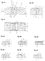
- FIG. 1A shows in cross section a plate 1 with a smooth contact surface 2 for receiving a Substrate 3.
- the substrate 3 is intermittently in a transport device, not shown Transport direction 4 advanced to a bond station, where it is either with a semiconductor chip or where wire connections between a mounted semiconductor chip and the substrate 3rd getting produced.
- the plate 1 has a bore 5 with a vacuum source that can be switched on and off connected is.
- the plate 1 contains a cavity 6 which is open against the support surface 2 and which Bore 5 surrounds. In the cavity 6 there is a flexible sealing element 7, for example in Shape of a thin membrane made of rubber.
- Fig. 1B shows the plate 1 in cross section to the transport direction along the line A-A of Fig. 1A.
- Line B-B denotes the position of the section shown in FIG. 1A.
- the substrate 3 is up arched.
- the curvature of the substrate 3 in its longitudinal direction which is the same as the transport direction 4, is less than its curvature transversely to the transport direction 4 and can only be seen in FIG. 1B.
- the longitudinal edges of the curved substrate 3 lie in the area of the suction device on the Plate 1 on.
- the IC shows the plate 1 and the substrate 3 in a top view.
- the suction device is for substrates 3 different widths suitable.
- the substrate 3 is not above the clarity of the drawing Suction device, but shown in the transport direction 4 next to the suction device.
- the sealing element 7 serves to more or between the bore 5 and the substrate 3 less well-sealing cavity to form, so that the substrate 3 when the cavity is acted upon is vacuumed onto the support surface 2 until it lies flat on the support surface 2. In order to If the sealing element 7 can fulfill this task, it must deal with the curvature of the substrate 3 can adjust.
- the sealing of the cavity may or may not be complete. To the Sucking in the substrate 3 is sufficient to limit the leakage rate of the cavity in such a way that between the top and bottom of the substrate 3, a pressure difference can be built up is sufficient to flatten the substrate 3.
- FIGS. 2A to 2C and FIGS. 3A to 3C schematically show the mode of operation of these according to the invention Suction device in the two cutting directions along the transport direction 4 or transversely to the transport direction 4.
- the sealing element touches 7 not yet the substrate 3: the space between the bore 5 and the substrate 3 forms no sealed cavity.
- 2B and 3B the state is shown in which the Sealing element 7 touches the substrate 3: There is a between the bore 5 and the substrate 3 sealed cavity 9 is formed.
- 2C and 3C show the state in which the bore 5 with Vacuum is applied. Since the cavity 9 seals sufficiently, the substrate 3 becomes atmospheric pressed against the support surface 2 and lies flat on the support surface 2. Now can the bonding process take place. After the vacuum is released, that in FIGS. 2A and 3A is formed again shown state and the substrate 3 can be transported further.
- the suction device shown in FIG. 1 is particularly advantageous.
- the cavity 6 is above a Hole 8 in connection with the outside world, so that there is atmospheric pressure in it.
- a suction on the sealing element 7 so that the sealing element 7 bends until it abuts the curved substrate 3.
- the sealing element 7 is namely, many times more elastic than the comparatively rigid substrate 3 the bore 5 and the substrate 3, the cavity 9 (FIG. 2B) is formed and it is built into the cavity 9 sufficiently large negative pressure or even vacuum with the effect that the substrate 3 from that its upper side prevailing atmospheric pressure is pressed against the support surface 2.
- a projection can also be provided, which the sealing element 7 in its cavity 6 holds.
- the cavity 6 could be drilled through the bore 8 if necessary Compressed air are supplied so that the sealing element 7 under the action of the compressed air bends and forms the cavity 9.
- the pressure of the compressed air only needs to be slightly above atmospheric pressure lie.
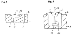
- FIG. 5 shows a further suction device, in which a circular sealing element 7 is provided is that can be supplied with a vacuum via a bore 11.
- the sealing element 7 is by means of of an electric or pneumatic drive 12 in the vertical direction 13 of one a raised position, typically about 2 mm, can be moved.
- the drive 12 serves the To bring sealing element 7 into contact with the still curved substrate 3.
- the edge of the Sealing element 7, which comes into contact with the substrate 3, is elastic designed so that the sealing element 7 when moving to the raised position of the curvature adapt the substrate 3 and form the sealing cavity 9 and thus subsequently the Substrate 3, when it is sucked against the plate 1, the edge of the sealing element 7 without problems can bend.
- the substrate 3 thus comes to rest flat on the support surface 2 of the plate 1, as soon as vacuum is applied to the bore 11, even if the drive the sealing element 7 is still in holds the raised position.
- the sealing element 7 is then before or after the bonding process lowered again.
- the sealing element 7 is resiliently mounted on the drive 12, so that the sucked substrate 3 can deflect the sealing element 7 against the drive 12.
Landscapes
- Engineering & Computer Science (AREA)
- Mechanical Engineering (AREA)
- Physics & Mathematics (AREA)
- Condensed Matter Physics & Semiconductors (AREA)
- General Physics & Mathematics (AREA)
- Manufacturing & Machinery (AREA)
- Computer Hardware Design (AREA)
- Microelectronics & Electronic Packaging (AREA)
- Power Engineering (AREA)
- Container, Conveyance, Adherence, Positioning, Of Wafer (AREA)
- Wire Bonding (AREA)
- Die Bonding (AREA)
Priority Applications (3)
| Application Number | Priority Date | Filing Date | Title |
|---|---|---|---|
| EP19990811159 EP1109207A1 (de) | 1999-12-14 | 1999-12-14 | Ansaugvorrichtung zum Niederhalten eines Substrates |
| JP2000379426A JP2001203222A (ja) | 1999-12-14 | 2000-12-13 | 湾曲した回路基板を水平に引きよせるとともに押しつける吸引装置を備えたダイボンダおよび/またはワイヤボンダ |
| EP00811195A EP1109205A1 (en) | 1999-12-14 | 2000-12-14 | Die bonder and/or wire bonder with a suction device for pulling flat and holding down a curved substrate |
Applications Claiming Priority (1)
| Application Number | Priority Date | Filing Date | Title |
|---|---|---|---|
| EP19990811159 EP1109207A1 (de) | 1999-12-14 | 1999-12-14 | Ansaugvorrichtung zum Niederhalten eines Substrates |
Publications (1)
| Publication Number | Publication Date |
|---|---|
| EP1109207A1 true EP1109207A1 (de) | 2001-06-20 |
Family
ID=8243188
Family Applications (1)
| Application Number | Title | Priority Date | Filing Date |
|---|---|---|---|
| EP19990811159 Withdrawn EP1109207A1 (de) | 1999-12-14 | 1999-12-14 | Ansaugvorrichtung zum Niederhalten eines Substrates |
Country Status (2)
| Country | Link |
|---|---|
| EP (1) | EP1109207A1 (enExample) |
| JP (1) | JP2001203222A (enExample) |
Cited By (1)
| Publication number | Priority date | Publication date | Assignee | Title |
|---|---|---|---|---|
| US7100501B2 (en) * | 2001-06-06 | 2006-09-05 | Gaming Partners International | Chip holding arrangement, pad printing system incorporating the arrangement, and method of pad printing a chip using the arrangement |
Families Citing this family (5)
| Publication number | Priority date | Publication date | Assignee | Title |
|---|---|---|---|---|
| US10541223B2 (en) * | 2017-05-05 | 2020-01-21 | Kulicke And Soffa Industries, Inc. | Methods of operating a wire bonding machine to improve clamping of a substrate, and wire bonding machines |
| TWI632982B (zh) * | 2017-07-03 | 2018-08-21 | 陽程科技股份有限公司 | Plate retaining device |
| CN111633589A (zh) * | 2020-06-16 | 2020-09-08 | 南京沃天科技有限公司 | 一种传感器芯片夹持固定结构 |
| CN112045750A (zh) * | 2020-08-25 | 2020-12-08 | 湖南亚太实业有限公司 | 一种吸塑件机械切割固定装置 |
| CN115415675A (zh) * | 2022-08-20 | 2022-12-02 | 北京力达塑料制造有限公司 | 一种用于安全帽加工的自动激光印刻系统 |
Citations (5)
| Publication number | Priority date | Publication date | Assignee | Title |
|---|---|---|---|---|
| GB2120141A (en) * | 1982-05-18 | 1983-11-30 | Gerber Scient Products Inc | Vacuum workpiece holder |
| EP0298564A1 (en) * | 1987-07-08 | 1989-01-11 | Philips and Du Pont Optical Company | Vacuum apparatus for holding workpieces |
| EP0456426A1 (en) * | 1990-05-07 | 1991-11-13 | Canon Kabushiki Kaisha | Vacuum type wafer holder |
| DE4024642A1 (de) * | 1990-08-03 | 1992-02-06 | Ibm | Schleuderteller fuer substrate |
| EP0565278A1 (en) * | 1992-04-06 | 1993-10-13 | AT&T Corp. | Wafer handling apparatus and method |
Family Cites Families (3)
| Publication number | Priority date | Publication date | Assignee | Title |
|---|---|---|---|---|
| JPH07193399A (ja) * | 1993-12-27 | 1995-07-28 | Hitachi Electron Eng Co Ltd | 配線基板の湾曲防止クランプ機構 |
| JP3348756B2 (ja) * | 1995-06-13 | 2002-11-20 | 山形カシオ株式会社 | 基板位置決め用吸着ピンユニット |
| JPH1117397A (ja) * | 1997-06-23 | 1999-01-22 | Matsushita Electric Ind Co Ltd | ワークの下受装置 |
-
1999
- 1999-12-14 EP EP19990811159 patent/EP1109207A1/de not_active Withdrawn
-
2000
- 2000-12-13 JP JP2000379426A patent/JP2001203222A/ja active Pending
Patent Citations (5)
| Publication number | Priority date | Publication date | Assignee | Title |
|---|---|---|---|---|
| GB2120141A (en) * | 1982-05-18 | 1983-11-30 | Gerber Scient Products Inc | Vacuum workpiece holder |
| EP0298564A1 (en) * | 1987-07-08 | 1989-01-11 | Philips and Du Pont Optical Company | Vacuum apparatus for holding workpieces |
| EP0456426A1 (en) * | 1990-05-07 | 1991-11-13 | Canon Kabushiki Kaisha | Vacuum type wafer holder |
| DE4024642A1 (de) * | 1990-08-03 | 1992-02-06 | Ibm | Schleuderteller fuer substrate |
| EP0565278A1 (en) * | 1992-04-06 | 1993-10-13 | AT&T Corp. | Wafer handling apparatus and method |
Cited By (1)
| Publication number | Priority date | Publication date | Assignee | Title |
|---|---|---|---|---|
| US7100501B2 (en) * | 2001-06-06 | 2006-09-05 | Gaming Partners International | Chip holding arrangement, pad printing system incorporating the arrangement, and method of pad printing a chip using the arrangement |
Also Published As
| Publication number | Publication date |
|---|---|
| JP2001203222A (ja) | 2001-07-27 |
Similar Documents
| Publication | Publication Date | Title |
|---|---|---|
| EP1321966B1 (de) | Greifwerkzeug zum Montieren von Halbleiterchips | |
| DE69015511T2 (de) | Verfahren und Vorrichtung zum Verbinden von Halbleitersubstraten. | |
| DE112018003709B4 (de) | Verfahren zum Herstellen eines LED-Moduls | |
| EP0267874B1 (de) | Verfahren zum Transportieren von perforierten plattenförmigen Objekten | |
| EP1257389B1 (de) | Vakuumhandhabungsgerät | |
| AT393827B (de) | Verfahren und vorrichtung zum fuellen einer isolierglaseinheit mit fuellgas | |
| DE102018100855A1 (de) | Endeffektor | |
| DE102008023907A1 (de) | Bernoulli-Greifvorrichtung zum Greifen und Handhaben von plattenförmigen Elementen, insbesondere von Waferelementen | |
| AT506622A2 (de) | Vorrichtung und verfahren zum aufbringen und/oder ablösen eines wafers auf einen/von einem träger | |
| EP1109207A1 (de) | Ansaugvorrichtung zum Niederhalten eines Substrates | |
| DE10059883A1 (de) | Die Bonder und/oder Wire Bonder mit einer Ansaugvorrichtung zum Flachziehen und Niederhalten eines gewölbten Substrats | |
| DE10227824B4 (de) | Verfahren und Vorrichtung zum Herstellen eines LCD | |
| DE19948572A1 (de) | Vorrichtung zum Handling von Halbleiterscheiben | |
| DE10390694T5 (de) | Halbleiterchip-Aufnahmevorrichtung | |
| EP1606836B1 (de) | Greifer und betriebsverfahren | |
| DE112015000945T5 (de) | Werkstückhaltegerät | |
| DE19625846A1 (de) | Vakuumgreifer zum Tragen eines Halbleiterwafers | |
| DE102009041969B4 (de) | Greifer für die Aufnahme, den Transport und die positionierte Ablage von streifenförmigen Elementen | |
| DE69231099T2 (de) | Befestigungsvorrichtung | |
| DE1506502A1 (de) | Hebe- und Transportvorrichtung fuer tafelartige,ebene Werkstuecke | |
| DE10050327A1 (de) | Saugnapf | |
| DE102004032604B4 (de) | Verfahren und Vorrichtung zum Zusammenbauen eines Solarzellenmoduls | |
| DE19528442A1 (de) | Schichtverbindungsverfahren | |
| DE2917252C2 (enExample) | ||
| DE10007642C2 (de) | Verfahren zum Trennen von Substraten im Nutzenformat mit vorgegebenen Sollbruchstellen |
Legal Events
| Date | Code | Title | Description |
|---|---|---|---|
| PUAI | Public reference made under article 153(3) epc to a published international application that has entered the european phase |
Free format text: ORIGINAL CODE: 0009012 |
|
| AK | Designated contracting states |
Kind code of ref document: A1 Designated state(s): AT BE CH CY DE DK ES FI FR GB GR IE IT LI LU MC NL PT SE |
|
| AX | Request for extension of the european patent |
Free format text: AL;LT;LV;MK;RO;SI |
|
| STAA | Information on the status of an ep patent application or granted ep patent |
Free format text: STATUS: THE APPLICATION HAS BEEN WITHDRAWN |
|
| 18W | Application withdrawn |
Withdrawal date: 20010627 |