EP1109207A1 - Ansaugvorrichtung zum Niederhalten eines Substrates - Google Patents
Ansaugvorrichtung zum Niederhalten eines Substrates Download PDFInfo
- Publication number
- EP1109207A1 EP1109207A1 EP19990811159 EP99811159A EP1109207A1 EP 1109207 A1 EP1109207 A1 EP 1109207A1 EP 19990811159 EP19990811159 EP 19990811159 EP 99811159 A EP99811159 A EP 99811159A EP 1109207 A1 EP1109207 A1 EP 1109207A1
- Authority
- EP
- European Patent Office
- Prior art keywords
- substrate
- cavity
- sealing element
- bore
- suction device
- Prior art date
- Legal status (The legal status is an assumption and is not a legal conclusion. Google has not performed a legal analysis and makes no representation as to the accuracy of the status listed.)
- Withdrawn
Links
Images
Classifications
-
- B—PERFORMING OPERATIONS; TRANSPORTING
- B25—HAND TOOLS; PORTABLE POWER-DRIVEN TOOLS; MANIPULATORS
- B25B—TOOLS OR BENCH DEVICES NOT OTHERWISE PROVIDED FOR, FOR FASTENING, CONNECTING, DISENGAGING OR HOLDING
- B25B11/00—Work holders not covered by any preceding group in the subclass, e.g. magnetic work holders, vacuum work holders
- B25B11/005—Vacuum work holders
-
- H—ELECTRICITY
- H01—ELECTRIC ELEMENTS
- H01L—SEMICONDUCTOR DEVICES NOT COVERED BY CLASS H10
- H01L21/00—Processes or apparatus adapted for the manufacture or treatment of semiconductor or solid state devices or of parts thereof
- H01L21/67—Apparatus specially adapted for handling semiconductor or electric solid state devices during manufacture or treatment thereof; Apparatus specially adapted for handling wafers during manufacture or treatment of semiconductor or electric solid state devices or components ; Apparatus not specifically provided for elsewhere
- H01L21/683—Apparatus specially adapted for handling semiconductor or electric solid state devices during manufacture or treatment thereof; Apparatus specially adapted for handling wafers during manufacture or treatment of semiconductor or electric solid state devices or components ; Apparatus not specifically provided for elsewhere for supporting or gripping
- H01L21/6838—Apparatus specially adapted for handling semiconductor or electric solid state devices during manufacture or treatment thereof; Apparatus specially adapted for handling wafers during manufacture or treatment of semiconductor or electric solid state devices or components ; Apparatus not specifically provided for elsewhere for supporting or gripping with gripping and holding devices using a vacuum; Bernoulli devices
-
- H—ELECTRICITY
- H01—ELECTRIC ELEMENTS
- H01L—SEMICONDUCTOR DEVICES NOT COVERED BY CLASS H10
- H01L2224/00—Indexing scheme for arrangements for connecting or disconnecting semiconductor or solid-state bodies and methods related thereto as covered by H01L24/00
- H01L2224/01—Means for bonding being attached to, or being formed on, the surface to be connected, e.g. chip-to-package, die-attach, "first-level" interconnects; Manufacturing methods related thereto
- H01L2224/42—Wire connectors; Manufacturing methods related thereto
- H01L2224/47—Structure, shape, material or disposition of the wire connectors after the connecting process
- H01L2224/48—Structure, shape, material or disposition of the wire connectors after the connecting process of an individual wire connector
- H01L2224/481—Disposition
- H01L2224/48151—Connecting between a semiconductor or solid-state body and an item not being a semiconductor or solid-state body, e.g. chip-to-substrate, chip-to-passive
- H01L2224/48221—Connecting between a semiconductor or solid-state body and an item not being a semiconductor or solid-state body, e.g. chip-to-substrate, chip-to-passive the body and the item being stacked
- H01L2224/48225—Connecting between a semiconductor or solid-state body and an item not being a semiconductor or solid-state body, e.g. chip-to-substrate, chip-to-passive the body and the item being stacked the item being non-metallic, e.g. insulating substrate with or without metallisation
- H01L2224/48227—Connecting between a semiconductor or solid-state body and an item not being a semiconductor or solid-state body, e.g. chip-to-substrate, chip-to-passive the body and the item being stacked the item being non-metallic, e.g. insulating substrate with or without metallisation connecting the wire to a bond pad of the item
Definitions
- the invention relates to a suction device for holding down a semiconductor chip populating or populating substrate of the type mentioned in the preamble of claim 1.
- Some substrates for example BGA®'s (Ball Grid Array) already equipped with semiconductor chips, which with a second semiconductor chip to be populated or for the production of wire connections Bond station of a wire bonder may be curved so strongly that the The substrate cannot be sucked in.
- the invention has for its object to provide a device that is also strongly curved Hold down substrates flat to the support surface.
- the invention is to vacuum the substrate as usual on its underside pressurize, but limit the leakage rate so that the vacuum between the can fill arched substrate and its contact surface. This is done by means of a sealing element a more or less well sealing cavity is formed in which to maintain the vacuum remains.
- the pressure difference between the pressure on the top of the substrate (atmospheric pressure) and the pressure on the bottom (vacuum) then causes the substrate to be flat against its base is pressed.
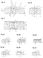
- FIG. 1A shows in cross section a plate 1 with a smooth contact surface 2 for receiving a Substrate 3.
- the substrate 3 is intermittently in a transport device, not shown Transport direction 4 advanced to a bond station, where it is either with a semiconductor chip or where wire connections between a mounted semiconductor chip and the substrate 3rd getting produced.
- the plate 1 has a bore 5 with a vacuum source that can be switched on and off connected is.
- the plate 1 contains a cavity 6 which is open against the support surface 2 and which Bore 5 surrounds. In the cavity 6 there is a flexible sealing element 7, for example in Shape of a thin membrane made of rubber.
- Fig. 1B shows the plate 1 in cross section to the transport direction along the line A-A of Fig. 1A.
- Line B-B denotes the position of the section shown in FIG. 1A.
- the substrate 3 is up arched.
- the curvature of the substrate 3 in its longitudinal direction which is the same as the transport direction 4, is less than its curvature transversely to the transport direction 4 and can only be seen in FIG. 1B.
- the longitudinal edges of the curved substrate 3 lie in the area of the suction device on the Plate 1 on.
- the IC shows the plate 1 and the substrate 3 in a top view.
- the suction device is for substrates 3 different widths suitable.
- the substrate 3 is not above the clarity of the drawing Suction device, but shown in the transport direction 4 next to the suction device.
- the sealing element 7 serves to more or between the bore 5 and the substrate 3 less well-sealing cavity to form, so that the substrate 3 when the cavity is acted upon is vacuumed onto the support surface 2 until it lies flat on the support surface 2. In order to If the sealing element 7 can fulfill this task, it must deal with the curvature of the substrate 3 can adjust.
- the sealing of the cavity may or may not be complete. To the Sucking in the substrate 3 is sufficient to limit the leakage rate of the cavity in such a way that between the top and bottom of the substrate 3, a pressure difference can be built up is sufficient to flatten the substrate 3.
- FIGS. 2A to 2C and FIGS. 3A to 3C schematically show the mode of operation of these according to the invention Suction device in the two cutting directions along the transport direction 4 or transversely to the transport direction 4.
- the sealing element touches 7 not yet the substrate 3: the space between the bore 5 and the substrate 3 forms no sealed cavity.
- 2B and 3B the state is shown in which the Sealing element 7 touches the substrate 3: There is a between the bore 5 and the substrate 3 sealed cavity 9 is formed.
- 2C and 3C show the state in which the bore 5 with Vacuum is applied. Since the cavity 9 seals sufficiently, the substrate 3 becomes atmospheric pressed against the support surface 2 and lies flat on the support surface 2. Now can the bonding process take place. After the vacuum is released, that in FIGS. 2A and 3A is formed again shown state and the substrate 3 can be transported further.
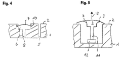
- the suction device shown in FIG. 1 is particularly advantageous.
- the cavity 6 is above a Hole 8 in connection with the outside world, so that there is atmospheric pressure in it.
- a suction on the sealing element 7 so that the sealing element 7 bends until it abuts the curved substrate 3.
- the sealing element 7 is namely, many times more elastic than the comparatively rigid substrate 3 the bore 5 and the substrate 3, the cavity 9 (FIG. 2B) is formed and it is built into the cavity 9 sufficiently large negative pressure or even vacuum with the effect that the substrate 3 from that its upper side prevailing atmospheric pressure is pressed against the support surface 2.
- a projection can also be provided, which the sealing element 7 in its cavity 6 holds.
- the cavity 6 could be drilled through the bore 8 if necessary Compressed air are supplied so that the sealing element 7 under the action of the compressed air bends and forms the cavity 9.
- the pressure of the compressed air only needs to be slightly above atmospheric pressure lie.
- FIG. 5 shows a further suction device, in which a circular sealing element 7 is provided is that can be supplied with a vacuum via a bore 11.
- the sealing element 7 is by means of of an electric or pneumatic drive 12 in the vertical direction 13 of one a raised position, typically about 2 mm, can be moved.
- the drive 12 serves the To bring sealing element 7 into contact with the still curved substrate 3.
- the edge of the Sealing element 7, which comes into contact with the substrate 3, is elastic designed so that the sealing element 7 when moving to the raised position of the curvature adapt the substrate 3 and form the sealing cavity 9 and thus subsequently the Substrate 3, when it is sucked against the plate 1, the edge of the sealing element 7 without problems can bend.
- the substrate 3 thus comes to rest flat on the support surface 2 of the plate 1, as soon as vacuum is applied to the bore 11, even if the drive the sealing element 7 is still in holds the raised position.
- the sealing element 7 is then before or after the bonding process lowered again.
- the sealing element 7 is resiliently mounted on the drive 12, so that the sucked substrate 3 can deflect the sealing element 7 against the drive 12.
Abstract
Eine Ansaugvorrichtung zum Niederhalten eines mit Halbleiterchips zu bestückenden oder bestückten Substrates (3) auf einer Auflagefläche (2) einer Platte (1) weist eine mit einer Vakuumquelle verbindbare Bohrung (5) zum Ansaugen des Substrates (3) auf. Die Platte (1) enthält eine gegen die Auflagefläche (2) offene Kavität (6). Die Kavität (6) weist ein flexibles Dichtungselement (7) auf zur Bildung eines abdichtenden Hohlraumes (9) zwischen dem Substrat (3) und der Bohrung (5). Sobald der abdichtende Hohlraum (9) gebildet ist, kann sich im Hohlraum (9) Vakuum ausbilden, so dass das Substrat (3) gegen die Auflagefläche (2) gesogen wird. <IMAGE> <IMAGE> <IMAGE>
Description
Die Erfindung betrifft eine Ansaugvorrichtung zum Niederhalten eines mit Halbleiterchips zu
bestückenden oder bestückten Substrates der im Oberbegriff des Anspruchs 1 genannten Art.
Bei der Montage von Halbleiterchips auf einem Substrat mittels eines sogenannten Die Bonders wird das
Substrat auf einer Auflagefläche taktweise um eine vorbestimmte Distanz transportiert, damit ein
Halbleiterchip an der dafür vorgesehenen Stelle montiert werden kann. Damit das Substrat plan auf der
Auflagefläche aufliegt, weist die Auflagefläche eine mit einer Vakuumquelle verbindbare Bohrung zum
Ansaugen und Niederhalten des Substrates auf.
Einige Substrate, beispielsweise bereits mit Halbleiterchips bestückte BGA®'s (Ball Grid Array), die mit
einem zweiten Halbleiterchip zu bestücken sind oder die zur Herstellung von Drahtverbindungen der
Bondstation eines Wire Bonders zugeführt werden, sind unter Umständen derart stark gewölbt, dass das
Ansaugen des Substrates nicht gelingt.
Der Erfindung liegt die Aufgabe zugrunde, eine Vorrichtung anzugeben, die auch stark gewölbte
Substrate plan zur Auflagefläche niederhalten kann.
Die Erfindung besteht in den im Anspruch 1 angegebenen Merkmalen. Vorteilhafte Ausgestaltungen
ergeben sich aus den abhängigen Ansprüchen.
Die Erfindung besteht darin, das Substrat wie gewohnt auf seiner Unterseite mit Vakuum zu
beaufschlagen, dabei aber die Leckrate zu begrenzen, damit das Vakuum den Raum zwischen dem
gewölbten Substrat und seiner Auflagefläche ausfüllen kann. Dazu wird mittels eines Dichtungselementes
ein mehr oder weniger gut abdichtender Hohlraum gebildet, in dem das Vakuum erhalten
bleibt. Die Druckdifferenz zwischen dem Druck auf der Oberseite des Substrates (Atmosphärendruck)
und dem Druck auf der Unterseite (Vakuum) bewirkt dann, dass das Substrat flach gegen seine Unterlage
gedrückt wird.
Nachfolgend werden Ausführungsbeispiele der Erfindung anhand der Zeichnung näher erläutert.
Es zeigen:
- Fig. 1A-C
- Schnittzeichnungen einer Platte mit einer Ansaugvorrichtung für ein Substrat,
- Fig. 2A-C und 3A-C
- verschiedene Zustände der Ansaugvorrichtung,
- Fig. 4
- ein Detail der Ansaugvorrichtung, und
- Fig. 5
- eine weitere Ansaugvorrichtung.
Die Fig. 1 A zeigt im Querschnitt eine Platte 1 mit einer glatten Auflagefläche 2 zur Aufnahme eines
Substrates 3. Das Substrat 3 wird von einer nicht dargestellten Transporteinrichtung taktweise in einer
Transportrichtung 4 zu einer Bondstation vorgeschoben, wo es entweder mit einem Halbleiterchip
bestückt wird oder wo Drahtverbindungen zwischen einem montierten Halbleiterchip und dem Substrat 3
hergestellt werden. Die Platte 1 weist eine Bohrung 5 auf, die mit einer ein- und ausschaltbaren Vakuumquelle
verbunden ist. Die Platte 1 enthält eine gegen die Auflagefläche 2 offene Kavität 6, die die
Bohrung 5 umgibt. In der Kavität 6 befindet sich ein flexibles Dichtungselement 7, beispielsweise in
Gestalt einer dünnen Membrane aus Gummi.
Die Fig. 1B zeigt die Platte 1 im Schnitt quer zur Transportrichtung entlang der Linie A-A der Fig. 1A.
Die Linie B-B bezeichnet die Lage des in der Fig. 1A gezeigten Schnittes. Das Substrat 3 ist nach oben
gewölbt. Die Wölbung des Substrates 3 in seiner Längsrichtung, die gleich der Transportrichtung 4 ist,
ist geringer als seine Wölbung quer zur Transportrichtung 4 und nur in der Fig. 1B ersichtlich. In der
Regel liegen die Längskanten des gewölbten Substrates 3 im Bereich der Ansaugvorrichtung auf der
Platte 1 auf. Zudem ist es üblich, das Substrat 3 im Bereich seiner Längskanten mittels Rollen gegen die
Platte 1 zu drücken.
Die Fig. IC zeigt die Platte 1 und das Substrat 3 in der Aufsicht. Die Ansaugvorrichtung ist für Substrate
3 unterschiedlicher Breite geeignet. Das Substrat 3 ist der Klarheit der Zeichnung wegen nicht über der
Ansaugvorrichtung, sondern in Transportrichtung 4 neben der Ansaugvorrichtung eingezeichnet.
Das Dichtungselement 7 dient dazu, zwischen der Bohrung 5 und dem Substrat 3 einen mehr oder
weniger gut abdichtenden Hohlraum zu bilden, damit das Substrat 3 bei Beaufschlagung des Hohlraumes
mit Vakuum auf die Auflagefläche 2 gesogen wird, bis es flach auf der Auflagefläche 2 aufliegt. Damit
das Dichtungselement 7 diese Aufgabe erfüllen kann, muss es sich der Wölbung des Substrates 3
anpassen können. Die Abdichtung des Hohlraumes kann, muss aber nicht vollständig sein. Zum
Ansaugen des Substrates 3 genügt es, die Leckrate des Hohlraumes derart zu begrenzen, dass zwischen
der Oberseite und der Unterseite des Substrates 3 eine Druckdifferenz aufgebaut werden kann, die
ausreicht, um das Substrat 3 flach zu drücken.
Bei dem gezeigten Beispiel ist eine einzige Kavität 6 mit einem einzigen Dichtungselement 7 vorhanden.
Es ist natürlich möglich, die Kavität 6, die in der Fig. 1A als zwei beidseitig der Bohrung 5 angeordnete
Vertiefungen erscheint, in zwei getrennte Kavitäten aufzutrennen und beide Kavitäten mit je einem
Dichtungselement 7 zu versehen.
Die Fig. 2A bis 2C und Fig. 3A bis 3C zeigen schematisch die Wirkungsweise dieser erfindungsgemässen
Ansaugvorrichtung in den beiden Schnittrichtungen längs der Transportrichtung 4 bzw. quer
zur Transportrichtung 4. Bei dem in den Fig. 2A und 3A gezeigten Zustand berührt das Dichtungselement
7 das Substrat 3 noch nicht: Der Raum zwischen der Bohrung 5 und dem Substrat 3 bildet
keinen abgedichteten Hohlraum. Bei den Fig. 2B und 3B ist der Zustand dargestellt, bei dem das
Dichtungselement 7 das Substrat 3 berührt: Zwischen der Bohrung 5 und dem Substrat 3 hat sich ein
abgedichteter Hohlraum 9 gebildet. Die Fig. 2C und 3C zeigen den Zustand, bei dem die Bohrung 5 mit
Vakuum beaufschlagt wird. Da der Hohlraum 9 genügend abdichtet, wird das Substrat 3 vom Atmosphärendruck
gegen die Auflagefläche 2 gedrückt und liegt flach auf der Auflagefläche 2 auf. Jetzt kann
der Bondvorgang erfolgen. Nach dem Lösen des Vakuums bildet sich wieder der in den Fig. 2A und 3A
gezeigte Zustand aus und das Substrat 3 kann weiter transportiert werden.
Es werden nun zwei Ausführungsbeispiele näher erläutert:
Die in der Fig. 1 gezeigte Ansaugvorrichtung ist besonders vorteilhaft. Die Kavität 6 steht über eine
Bohrung 8 mit der Aussenwelt in Verbindung, so dass in ihr atmosphärischer Druck herrscht. Beim
Anlegen von Vakuum an die Bohrung 5 bewirkt die Druckdifferenz zwischen dem Druck in der Kavität
6 (Atmosphärendruck) und der Bohrung 5 (Vakuum) einen Sog auf das Dichtungselement 7, so dass sich
das Dichtungselement 7 biegt, bis es am gewölbten Substrat 3 anliegt. Das Dichtungselement 7 ist
nämlich um ein Vielfaches elastischer als das vergleichsweise starre Substrat 3. Jetzt hat sich zwischen
der Bohrung 5 und dem Substrat 3 der Hohlraum 9 (Fig. 2B) gebildet und es baut sich im Hohlraum 9 ein
genügend grosser Unterdruck oder sogar Vakuum auf mit der Wirkung, dass das Substrat 3 von dem auf
seiner Oberseite herrschenden Atmosphärendruck gegen die Auflagefläche 2 gedrückt wird.
Damit das Dichtungselement 7 beim Transport des Substrates 3 nicht ungewollt mitgezerrt wird, ist die
Kavität 6, wie in der Fig. 4 gezeigt ist, bevorzugt mit einer umlaufenden Nut 10 ausgebildet, in der das
Dichtungselement 7 entweder lose eingelegt oder zumindest auf der der Bohrung 5 zugewandten Seite
der Kavität 6 luftdicht befestigt ist. Sobald Vakuum an die Bohrung 5 angelegt wird, bewirkt der auf das
Dichtungselement 7 einwirkende Sog eine Wölbung des Dichtungselementes 7, bis es das Substrat 3
berührt. Anstelle der Nut 10 kann auch ein Vorsprung vorgesehen sein, der das Dichtungselement 7 in
seiner Kavität 6 hält.
Obwohl die Sogwirkung in der Regel ausreicht, könnte der Kavität 6 bei Bedarf über die Bohrung 8
Druckluft zugeführt werden, so dass sich das Dichtungselement 7 unter der Wirkung der Druckluft
verbiegt und den Hohlraum 9 bildet. Der Druck der Druckluft muss dazu nur leicht über dem Atmosphärendruck
liegen.
Die Fig. 5 zeigt eine weitere Ansaugvorrichtung, bei der ein kreisrundes Dichtungselement 7 vorgesehen
ist, das über eine Bohrung 11 mit Vakuum beaufschlagt werden kann. Das Dichtungselement 7 ist mittels
eines elektrischen oder pneumatischen Antriebes 12 in vertikaler Richtung 13 von einer abgesen
eine angehobene Position, typisch um etwa 2 mm, verschiebbar. Der Antrieb 12 dient dazu, das
Dichtungselement 7 in Berührung mit dem noch gewölbten Substrat 3 zu bringen. Der Rand des
Dichtungselementes 7, der jeweils mit dem Substrat 3 in Berührung kommt, ist dabei elastisch
ausgestaltet, damit sich das Dichtungselement 7 beim Anfahren der angehobenen Position der Wölbung
des Substrates 3 anpassen und den abdichtenden Hohlraum 9 bilden kann und damit anschliessend das
Substrat 3, wenn es gegen die Platte 1 gesogen wird, den Rand des Dichtungselementes 7 problemlos
verbiegen kann. Das Substrat 3 kommt somit flach auf der Auflagefläche 2 der Platte 1 zur Auflage,
sobald Vakuum an die Bohrung 11 gelegt wird, selbst wenn der Antrieb das Dichtungselement 7 noch in
der angehobenen Position hält. Das Dichtungselement 7 wird dann vor oder nach dem Bondvorgang
wieder abgesenkt. Bei einer anderen Lösung ist das Dichtungselement 7 federnd am Antrieb 12 gelagert,
so dass das angesogene Substrat 3 das Dichtungselement 7 gegen den Antrieb 12 einfedern kann.
Claims (3)
- Ansaugvorrichtung zum Niederhalten eines mit Halbleiterchips zu bestückenden oder bestückten Substrates (3) auf einer Auflagefläche (2) einer Platte (1), die eine mit einer Vakuumquelle verbindbare Bohrung (5) zum Ansaugen des Substrates (3) aufweist, dadurch gekennzeichnet, dass die Platte (1) eine gegen die Auflagefläche (2) offene Kavität (6) enthält und dass die Kavität (6) ein Dichtungselement (7) zur Bildung eines Hohlraumes (9) zwischen dem Substrat (3) und der Bohrung (5) aufweist.
- Ansaugvorrichtung nach Anspruch 1, dadurch gekennzeichnet, dass die Kavität (6) druckmässig mit der Aussenwelt in Verbindung steht.
- Ansaugvorrichtung nach Anspruch 1 oder 2, dadurch gekennzeichnet, dass das Dichtungselement (7) mittels eines Antriebes heb- und senkbar ist.
Priority Applications (3)
| Application Number | Priority Date | Filing Date | Title |
|---|---|---|---|
| EP19990811159 EP1109207A1 (de) | 1999-12-14 | 1999-12-14 | Ansaugvorrichtung zum Niederhalten eines Substrates |
| JP2000379426A JP2001203222A (ja) | 1999-12-14 | 2000-12-13 | 湾曲した回路基板を水平に引きよせるとともに押しつける吸引装置を備えたダイボンダおよび/またはワイヤボンダ |
| EP00811195A EP1109205A1 (de) | 1999-12-14 | 2000-12-14 | Die Bonder und/oder Wire Bonder mit einer Ansaugvorrichtung zum Flachziehen und Niederhalten eines gewölbten Substrats |
Applications Claiming Priority (1)
| Application Number | Priority Date | Filing Date | Title |
|---|---|---|---|
| EP19990811159 EP1109207A1 (de) | 1999-12-14 | 1999-12-14 | Ansaugvorrichtung zum Niederhalten eines Substrates |
Publications (1)
| Publication Number | Publication Date |
|---|---|
| EP1109207A1 true EP1109207A1 (de) | 2001-06-20 |
Family
ID=8243188
Family Applications (1)
| Application Number | Title | Priority Date | Filing Date |
|---|---|---|---|
| EP19990811159 Withdrawn EP1109207A1 (de) | 1999-12-14 | 1999-12-14 | Ansaugvorrichtung zum Niederhalten eines Substrates |
Country Status (2)
| Country | Link |
|---|---|
| EP (1) | EP1109207A1 (de) |
| JP (1) | JP2001203222A (de) |
Cited By (1)
| Publication number | Priority date | Publication date | Assignee | Title |
|---|---|---|---|---|
| US7100501B2 (en) * | 2001-06-06 | 2006-09-05 | Gaming Partners International | Chip holding arrangement, pad printing system incorporating the arrangement, and method of pad printing a chip using the arrangement |
Families Citing this family (4)
| Publication number | Priority date | Publication date | Assignee | Title |
|---|---|---|---|---|
| US10541223B2 (en) * | 2017-05-05 | 2020-01-21 | Kulicke And Soffa Industries, Inc. | Methods of operating a wire bonding machine to improve clamping of a substrate, and wire bonding machines |
| TWI632982B (zh) * | 2017-07-03 | 2018-08-21 | 陽程科技股份有限公司 | Plate retaining device |
| CN111633589A (zh) * | 2020-06-16 | 2020-09-08 | 南京沃天科技有限公司 | 一种传感器芯片夹持固定结构 |
| CN112045750A (zh) * | 2020-08-25 | 2020-12-08 | 湖南亚太实业有限公司 | 一种吸塑件机械切割固定装置 |
Citations (5)
| Publication number | Priority date | Publication date | Assignee | Title |
|---|---|---|---|---|
| GB2120141A (en) * | 1982-05-18 | 1983-11-30 | Gerber Scient Products Inc | Vacuum workpiece holder |
| EP0298564A1 (de) * | 1987-07-08 | 1989-01-11 | Philips and Du Pont Optical Company | Vakuumvorrichtung zum Halten von Werkstücken |
| EP0456426A1 (de) * | 1990-05-07 | 1991-11-13 | Canon Kabushiki Kaisha | Substratträger des Vakuumtyps |
| DE4024642A1 (de) * | 1990-08-03 | 1992-02-06 | Ibm | Schleuderteller fuer substrate |
| EP0565278A1 (de) * | 1992-04-06 | 1993-10-13 | AT&T Corp. | Vorrichtug zur Handhabung von Halbleiter-Platten und Verfahren |
-
1999
- 1999-12-14 EP EP19990811159 patent/EP1109207A1/de not_active Withdrawn
-
2000
- 2000-12-13 JP JP2000379426A patent/JP2001203222A/ja active Pending
Patent Citations (5)
| Publication number | Priority date | Publication date | Assignee | Title |
|---|---|---|---|---|
| GB2120141A (en) * | 1982-05-18 | 1983-11-30 | Gerber Scient Products Inc | Vacuum workpiece holder |
| EP0298564A1 (de) * | 1987-07-08 | 1989-01-11 | Philips and Du Pont Optical Company | Vakuumvorrichtung zum Halten von Werkstücken |
| EP0456426A1 (de) * | 1990-05-07 | 1991-11-13 | Canon Kabushiki Kaisha | Substratträger des Vakuumtyps |
| DE4024642A1 (de) * | 1990-08-03 | 1992-02-06 | Ibm | Schleuderteller fuer substrate |
| EP0565278A1 (de) * | 1992-04-06 | 1993-10-13 | AT&T Corp. | Vorrichtug zur Handhabung von Halbleiter-Platten und Verfahren |
Cited By (1)
| Publication number | Priority date | Publication date | Assignee | Title |
|---|---|---|---|---|
| US7100501B2 (en) * | 2001-06-06 | 2006-09-05 | Gaming Partners International | Chip holding arrangement, pad printing system incorporating the arrangement, and method of pad printing a chip using the arrangement |
Also Published As
| Publication number | Publication date |
|---|---|
| JP2001203222A (ja) | 2001-07-27 |
Similar Documents
| Publication | Publication Date | Title |
|---|---|---|
| EP1321966B1 (de) | Greifwerkzeug zum Montieren von Halbleiterchips | |
| EP0267874B1 (de) | Verfahren zum Transportieren von perforierten plattenförmigen Objekten | |
| EP1257389B1 (de) | Vakuumhandhabungsgerät | |
| AT519587B1 (de) | Saugvorrichtung für einen Endeffektor, Endeffektor zum Halten von Substraten sowie Verfahren zur Herstellung eines Endeffektors | |
| AT511627B1 (de) | Vorrichtung zum halten eines flächigen substrats | |
| AT519588B1 (de) | Endeffektor | |
| AT506622B1 (de) | Vorrichtung und verfahren zum aufbringen und/oder ablösen eines wafers auf einen/von einem träger | |
| DE102008023907A1 (de) | Bernoulli-Greifvorrichtung zum Greifen und Handhaben von plattenförmigen Elementen, insbesondere von Waferelementen | |
| DE10059883A1 (de) | Die Bonder und/oder Wire Bonder mit einer Ansaugvorrichtung zum Flachziehen und Niederhalten eines gewölbten Substrats | |
| EP1109207A1 (de) | Ansaugvorrichtung zum Niederhalten eines Substrates | |
| DE10390694T5 (de) | Halbleiterchip-Aufnahmevorrichtung | |
| DE112015000945T5 (de) | Werkstückhaltegerät | |
| DE102017120243B4 (de) | Verfahren und Vorrichtung zum Applizieren einer Komponente an einem Bauteil mittels eines Manipulators | |
| EP1332516A1 (de) | Verfahren zum aufbringen eines substrats | |
| EP1606836B1 (de) | Greifer und betriebsverfahren | |
| DE19625846A1 (de) | Vakuumgreifer zum Tragen eines Halbleiterwafers | |
| EP1796451B1 (de) | Stützstift zum Unterstützen eines mit elektrischen Bauteilen zu bestückenden Substrats | |
| DE102004032604B4 (de) | Verfahren und Vorrichtung zum Zusammenbauen eines Solarzellenmoduls | |
| EP0373395A2 (de) | Verfahren und Vorrichtung zur Ausbildung eines behälterförmigen Folienkörpers | |
| DE19528442A1 (de) | Schichtverbindungsverfahren | |
| DE2917252C2 (de) | ||
| DE10007642C2 (de) | Verfahren zum Trennen von Substraten im Nutzenformat mit vorgegebenen Sollbruchstellen | |
| WO2002067295A1 (de) | Verfahren und vorrichtungen zum ablösen eines halbleiterwafers von einem träger | |
| EP1558425A2 (de) | Vorrichtung und verfahren für das verbinden von objekten | |
| EP3185075A1 (de) | Vorrichtung für belichtungssystem |
Legal Events
| Date | Code | Title | Description |
|---|---|---|---|
| PUAI | Public reference made under article 153(3) epc to a published international application that has entered the european phase |
Free format text: ORIGINAL CODE: 0009012 |
|
| AK | Designated contracting states |
Kind code of ref document: A1 Designated state(s): AT BE CH CY DE DK ES FI FR GB GR IE IT LI LU MC NL PT SE |
|
| AX | Request for extension of the european patent |
Free format text: AL;LT;LV;MK;RO;SI |
|
| STAA | Information on the status of an ep patent application or granted ep patent |
Free format text: STATUS: THE APPLICATION HAS BEEN WITHDRAWN |
|
| 18W | Application withdrawn |
Withdrawal date: 20010627 |