EP1102254A1 - Method for producing master disk for producing formed substrate with groove, method for producing stamper for producing formed substrate with groove, method for producing formed substrate with groove, formed substrate with groove, storage medium, storage, and computer - Google Patents
Method for producing master disk for producing formed substrate with groove, method for producing stamper for producing formed substrate with groove, method for producing formed substrate with groove, formed substrate with groove, storage medium, storage, and computer Download PDFInfo
- Publication number
- EP1102254A1 EP1102254A1 EP99926771A EP99926771A EP1102254A1 EP 1102254 A1 EP1102254 A1 EP 1102254A1 EP 99926771 A EP99926771 A EP 99926771A EP 99926771 A EP99926771 A EP 99926771A EP 1102254 A1 EP1102254 A1 EP 1102254A1
- Authority
- EP
- European Patent Office
- Prior art keywords
- substrate
- photoresist
- grooved molding
- stamper
- molding substrate
- Prior art date
- Legal status (The legal status is an assumption and is not a legal conclusion. Google has not performed a legal analysis and makes no representation as to the accuracy of the status listed.)
- Withdrawn
Links
- 239000000758 substrate Substances 0.000 title claims abstract description 398
- 238000004519 manufacturing process Methods 0.000 title claims description 75
- 238000003860 storage Methods 0.000 title description 4
- 238000000465 moulding Methods 0.000 claims abstract description 180
- 238000000034 method Methods 0.000 claims abstract description 124
- 229920002120 photoresistant polymer Polymers 0.000 claims abstract description 112
- 229920005989 resin Polymers 0.000 claims abstract description 103
- 239000011347 resin Substances 0.000 claims abstract description 103
- 238000005323 electroforming Methods 0.000 claims abstract description 28
- 239000011521 glass Substances 0.000 claims abstract description 28
- 238000005530 etching Methods 0.000 claims description 24
- 229910052751 metal Inorganic materials 0.000 claims description 22
- 239000002184 metal Substances 0.000 claims description 22
- 230000015654 memory Effects 0.000 claims description 17
- 238000001746 injection moulding Methods 0.000 claims description 12
- 230000003287 optical effect Effects 0.000 abstract description 29
- 238000000926 separation method Methods 0.000 abstract description 7
- 239000010410 layer Substances 0.000 description 63
- 238000007747 plating Methods 0.000 description 30
- 239000000463 material Substances 0.000 description 25
- 239000000243 solution Substances 0.000 description 24
- PXHVJJICTQNCMI-UHFFFAOYSA-N Nickel Chemical compound [Ni] PXHVJJICTQNCMI-UHFFFAOYSA-N 0.000 description 21
- 230000003746 surface roughness Effects 0.000 description 20
- 239000002344 surface layer Substances 0.000 description 12
- -1 for example Polymers 0.000 description 9
- 238000001020 plasma etching Methods 0.000 description 9
- 238000009713 electroplating Methods 0.000 description 8
- 239000007788 liquid Substances 0.000 description 8
- 230000005855 radiation Effects 0.000 description 8
- 229920001187 thermosetting polymer Polymers 0.000 description 8
- 229910010293 ceramic material Inorganic materials 0.000 description 7
- VYPSYNLAJGMNEJ-UHFFFAOYSA-N silicon dioxide Inorganic materials O=[Si]=O VYPSYNLAJGMNEJ-UHFFFAOYSA-N 0.000 description 7
- 238000004544 sputter deposition Methods 0.000 description 7
- XKRFYHLGVUSROY-UHFFFAOYSA-N Argon Chemical compound [Ar] XKRFYHLGVUSROY-UHFFFAOYSA-N 0.000 description 6
- 239000006087 Silane Coupling Agent Substances 0.000 description 6
- 239000011248 coating agent Substances 0.000 description 6
- 238000000576 coating method Methods 0.000 description 6
- 238000001465 metallisation Methods 0.000 description 6
- 229920000515 polycarbonate Polymers 0.000 description 6
- 239000004417 polycarbonate Substances 0.000 description 6
- 230000002829 reductive effect Effects 0.000 description 6
- 238000005286 illumination Methods 0.000 description 5
- 150000002739 metals Chemical class 0.000 description 5
- 238000005498 polishing Methods 0.000 description 5
- 239000011253 protective coating Substances 0.000 description 5
- 239000002904 solvent Substances 0.000 description 5
- 239000004793 Polystyrene Substances 0.000 description 4
- 229910045601 alloy Inorganic materials 0.000 description 4
- 239000000956 alloy Substances 0.000 description 4
- 239000000919 ceramic Substances 0.000 description 4
- 238000001312 dry etching Methods 0.000 description 4
- 238000001035 drying Methods 0.000 description 4
- 239000000203 mixture Substances 0.000 description 4
- 229920000098 polyolefin Polymers 0.000 description 4
- 229920002223 polystyrene Polymers 0.000 description 4
- 239000010453 quartz Substances 0.000 description 4
- 229920005992 thermoplastic resin Polymers 0.000 description 4
- 238000005406 washing Methods 0.000 description 4
- NIXOWILDQLNWCW-UHFFFAOYSA-M Acrylate Chemical compound [O-]C(=O)C=C NIXOWILDQLNWCW-UHFFFAOYSA-M 0.000 description 3
- LFQSCWFLJHTTHZ-UHFFFAOYSA-N Ethanol Chemical compound CCO LFQSCWFLJHTTHZ-UHFFFAOYSA-N 0.000 description 3
- OKKJLVBELUTLKV-UHFFFAOYSA-N Methanol Chemical compound OC OKKJLVBELUTLKV-UHFFFAOYSA-N 0.000 description 3
- HEMHJVSKTPXQMS-UHFFFAOYSA-M Sodium hydroxide Chemical compound [OH-].[Na+] HEMHJVSKTPXQMS-UHFFFAOYSA-M 0.000 description 3
- YXFVVABEGXRONW-UHFFFAOYSA-N Toluene Chemical compound CC1=CC=CC=C1 YXFVVABEGXRONW-UHFFFAOYSA-N 0.000 description 3
- 229910052782 aluminium Inorganic materials 0.000 description 3
- 229910052786 argon Inorganic materials 0.000 description 3
- 230000015572 biosynthetic process Effects 0.000 description 3
- 150000001875 compounds Chemical class 0.000 description 3
- 229910052802 copper Inorganic materials 0.000 description 3
- 239000010949 copper Substances 0.000 description 3
- 238000000151 deposition Methods 0.000 description 3
- 230000008021 deposition Effects 0.000 description 3
- 238000010586 diagram Methods 0.000 description 3
- 230000005611 electricity Effects 0.000 description 3
- 238000005516 engineering process Methods 0.000 description 3
- 239000012467 final product Substances 0.000 description 3
- 238000007733 ion plating Methods 0.000 description 3
- 238000002844 melting Methods 0.000 description 3
- 239000003504 photosensitizing agent Substances 0.000 description 3
- 229920000193 polymethacrylate Polymers 0.000 description 3
- 239000002994 raw material Substances 0.000 description 3
- 230000001172 regenerating effect Effects 0.000 description 3
- 230000035945 sensitivity Effects 0.000 description 3
- 150000004756 silanes Chemical class 0.000 description 3
- 229910052709 silver Inorganic materials 0.000 description 3
- 238000004528 spin coating Methods 0.000 description 3
- 239000012956 1-hydroxycyclohexylphenyl-ketone Substances 0.000 description 2
- HDYFAPRLDWYIBU-UHFFFAOYSA-N 1-silylprop-2-en-1-one Chemical class [SiH3]C(=O)C=C HDYFAPRLDWYIBU-UHFFFAOYSA-N 0.000 description 2
- CSCPPACGZOOCGX-UHFFFAOYSA-N Acetone Chemical compound CC(C)=O CSCPPACGZOOCGX-UHFFFAOYSA-N 0.000 description 2
- 239000004925 Acrylic resin Substances 0.000 description 2
- BSYNRYMUTXBXSQ-UHFFFAOYSA-N Aspirin Chemical compound CC(=O)OC1=CC=CC=C1C(O)=O BSYNRYMUTXBXSQ-UHFFFAOYSA-N 0.000 description 2
- 239000004593 Epoxy Substances 0.000 description 2
- MHAJPDPJQMAIIY-UHFFFAOYSA-N Hydrogen peroxide Chemical compound OO MHAJPDPJQMAIIY-UHFFFAOYSA-N 0.000 description 2
- KFZMGEQAYNKOFK-UHFFFAOYSA-N Isopropanol Chemical compound CC(C)O KFZMGEQAYNKOFK-UHFFFAOYSA-N 0.000 description 2
- ATJFFYVFTNAWJD-UHFFFAOYSA-N Tin Chemical compound [Sn] ATJFFYVFTNAWJD-UHFFFAOYSA-N 0.000 description 2
- GWEVSGVZZGPLCZ-UHFFFAOYSA-N Titan oxide Chemical compound O=[Ti]=O GWEVSGVZZGPLCZ-UHFFFAOYSA-N 0.000 description 2
- 150000001252 acrylic acid derivatives Chemical class 0.000 description 2
- 238000004380 ashing Methods 0.000 description 2
- MQDJYUACMFCOFT-UHFFFAOYSA-N bis[2-(1-hydroxycyclohexyl)phenyl]methanone Chemical compound C=1C=CC=C(C(=O)C=2C(=CC=CC=2)C2(O)CCCCC2)C=1C1(O)CCCCC1 MQDJYUACMFCOFT-UHFFFAOYSA-N 0.000 description 2
- 239000003054 catalyst Substances 0.000 description 2
- 239000003795 chemical substances by application Substances 0.000 description 2
- 229910052804 chromium Inorganic materials 0.000 description 2
- 238000004140 cleaning Methods 0.000 description 2
- 239000013065 commercial product Substances 0.000 description 2
- 230000007423 decrease Effects 0.000 description 2
- 230000003247 decreasing effect Effects 0.000 description 2
- 238000009826 distribution Methods 0.000 description 2
- 230000000694 effects Effects 0.000 description 2
- 239000003822 epoxy resin Substances 0.000 description 2
- 239000005357 flat glass Substances 0.000 description 2
- LNEPOXFFQSENCJ-UHFFFAOYSA-N haloperidol Chemical compound C1CC(O)(C=2C=CC(Cl)=CC=2)CCN1CCCC(=O)C1=CC=C(F)C=C1 LNEPOXFFQSENCJ-UHFFFAOYSA-N 0.000 description 2
- 238000010438 heat treatment Methods 0.000 description 2
- 238000001198 high resolution scanning electron microscopy Methods 0.000 description 2
- 238000002347 injection Methods 0.000 description 2
- 239000007924 injection Substances 0.000 description 2
- 150000002500 ions Chemical class 0.000 description 2
- 238000003698 laser cutting Methods 0.000 description 2
- 239000004973 liquid crystal related substance Substances 0.000 description 2
- 229910052759 nickel Inorganic materials 0.000 description 2
- KERTUBUCQCSNJU-UHFFFAOYSA-L nickel(2+);disulfamate Chemical compound [Ni+2].NS([O-])(=O)=O.NS([O-])(=O)=O KERTUBUCQCSNJU-UHFFFAOYSA-L 0.000 description 2
- 229920001778 nylon Polymers 0.000 description 2
- 229910052697 platinum Inorganic materials 0.000 description 2
- 229920000647 polyepoxide Polymers 0.000 description 2
- 229920000728 polyester Polymers 0.000 description 2
- 229920000642 polymer Polymers 0.000 description 2
- 238000006116 polymerization reaction Methods 0.000 description 2
- 239000004814 polyurethane Substances 0.000 description 2
- 229920002635 polyurethane Polymers 0.000 description 2
- 229920000915 polyvinyl chloride Polymers 0.000 description 2
- 238000003825 pressing Methods 0.000 description 2
- 239000000047 product Substances 0.000 description 2
- 239000004065 semiconductor Substances 0.000 description 2
- FZHAPNGMFPVSLP-UHFFFAOYSA-N silanamine Chemical class [SiH3]N FZHAPNGMFPVSLP-UHFFFAOYSA-N 0.000 description 2
- 230000003068 static effect Effects 0.000 description 2
- 229910052718 tin Inorganic materials 0.000 description 2
- 229910052719 titanium Inorganic materials 0.000 description 2
- 229910021642 ultra pure water Inorganic materials 0.000 description 2
- 239000012498 ultrapure water Substances 0.000 description 2
- UKRDPEFKFJNXQM-UHFFFAOYSA-N vinylsilane Chemical class [SiH3]C=C UKRDPEFKFJNXQM-UHFFFAOYSA-N 0.000 description 2
- WYTZZXDRDKSJID-UHFFFAOYSA-N (3-aminopropyl)triethoxysilane Chemical compound CCO[Si](OCC)(OCC)CCCN WYTZZXDRDKSJID-UHFFFAOYSA-N 0.000 description 1
- OXYZDRAJMHGSMW-UHFFFAOYSA-N 3-chloropropyl(trimethoxy)silane Chemical compound CO[Si](OC)(OC)CCCCl OXYZDRAJMHGSMW-UHFFFAOYSA-N 0.000 description 1
- UUEWCQRISZBELL-UHFFFAOYSA-N 3-trimethoxysilylpropane-1-thiol Chemical compound CO[Si](OC)(OC)CCCS UUEWCQRISZBELL-UHFFFAOYSA-N 0.000 description 1
- XDLMVUHYZWKMMD-UHFFFAOYSA-N 3-trimethoxysilylpropyl 2-methylprop-2-enoate Chemical compound CO[Si](OC)(OC)CCCOC(=O)C(C)=C XDLMVUHYZWKMMD-UHFFFAOYSA-N 0.000 description 1
- 229920000178 Acrylic resin Polymers 0.000 description 1
- 229910017083 AlN Inorganic materials 0.000 description 1
- 239000005046 Chlorosilane Substances 0.000 description 1
- VYZAMTAEIAYCRO-UHFFFAOYSA-N Chromium Chemical compound [Cr] VYZAMTAEIAYCRO-UHFFFAOYSA-N 0.000 description 1
- 229910019222 CoCrPt Inorganic materials 0.000 description 1
- 229910000684 Cobalt-chrome Inorganic materials 0.000 description 1
- RYGMFSIKBFXOCR-UHFFFAOYSA-N Copper Chemical compound [Cu] RYGMFSIKBFXOCR-UHFFFAOYSA-N 0.000 description 1
- 229910018104 Ni-P Inorganic materials 0.000 description 1
- GRYLNZFGIOXLOG-UHFFFAOYSA-N Nitric acid Chemical compound O[N+]([O-])=O GRYLNZFGIOXLOG-UHFFFAOYSA-N 0.000 description 1
- 229910018536 Ni—P Inorganic materials 0.000 description 1
- CTQNGGLPUBDAKN-UHFFFAOYSA-N O-Xylene Chemical compound CC1=CC=CC=C1C CTQNGGLPUBDAKN-UHFFFAOYSA-N 0.000 description 1
- CBENFWSGALASAD-UHFFFAOYSA-N Ozone Chemical compound [O-][O+]=O CBENFWSGALASAD-UHFFFAOYSA-N 0.000 description 1
- 239000004743 Polypropylene Substances 0.000 description 1
- 229910052581 Si3N4 Inorganic materials 0.000 description 1
- BQCADISMDOOEFD-UHFFFAOYSA-N Silver Chemical compound [Ag] BQCADISMDOOEFD-UHFFFAOYSA-N 0.000 description 1
- 235000000126 Styrax benzoin Nutrition 0.000 description 1
- 244000028419 Styrax benzoin Species 0.000 description 1
- 235000008411 Sumatra benzointree Nutrition 0.000 description 1
- 229910004160 TaO2 Inorganic materials 0.000 description 1
- 239000004433 Thermoplastic polyurethane Substances 0.000 description 1
- 229910008479 TiSi2 Inorganic materials 0.000 description 1
- UMVBXBACMIOFDO-UHFFFAOYSA-N [N].[Si] Chemical class [N].[Si] UMVBXBACMIOFDO-UHFFFAOYSA-N 0.000 description 1
- 238000010521 absorption reaction Methods 0.000 description 1
- DHKHKXVYLBGOIT-UHFFFAOYSA-N acetaldehyde Diethyl Acetal Natural products CCOC(C)OCC DHKHKXVYLBGOIT-UHFFFAOYSA-N 0.000 description 1
- 150000008062 acetophenones Chemical class 0.000 description 1
- 239000002253 acid Substances 0.000 description 1
- 239000003929 acidic solution Substances 0.000 description 1
- 230000002411 adverse Effects 0.000 description 1
- 239000012670 alkaline solution Substances 0.000 description 1
- XAGFODPZIPBFFR-UHFFFAOYSA-N aluminium Chemical compound [Al] XAGFODPZIPBFFR-UHFFFAOYSA-N 0.000 description 1
- PNEYBMLMFCGWSK-UHFFFAOYSA-N aluminium oxide Inorganic materials [O-2].[O-2].[O-2].[Al+3].[Al+3] PNEYBMLMFCGWSK-UHFFFAOYSA-N 0.000 description 1
- 239000005354 aluminosilicate glass Substances 0.000 description 1
- 150000004056 anthraquinones Chemical class 0.000 description 1
- 230000003466 anti-cipated effect Effects 0.000 description 1
- 239000002216 antistatic agent Substances 0.000 description 1
- QVGXLLKOCUKJST-UHFFFAOYSA-N atomic oxygen Chemical compound [O] QVGXLLKOCUKJST-UHFFFAOYSA-N 0.000 description 1
- 229960002130 benzoin Drugs 0.000 description 1
- DFJQEGUNXWZVAH-UHFFFAOYSA-N bis($l^{2}-silanylidene)titanium Chemical compound [Si]=[Ti]=[Si] DFJQEGUNXWZVAH-UHFFFAOYSA-N 0.000 description 1
- SYFOAKAXGNMQAX-UHFFFAOYSA-N bis(prop-2-enyl) carbonate;2-(2-hydroxyethoxy)ethanol Chemical compound OCCOCCO.C=CCOC(=O)OCC=C SYFOAKAXGNMQAX-UHFFFAOYSA-N 0.000 description 1
- DQXBYHZEEUGOBF-UHFFFAOYSA-N but-3-enoic acid;ethene Chemical compound C=C.OC(=O)CC=C DQXBYHZEEUGOBF-UHFFFAOYSA-N 0.000 description 1
- AXCZMVOFGPJBDE-UHFFFAOYSA-L calcium dihydroxide Chemical compound [OH-].[OH-].[Ca+2] AXCZMVOFGPJBDE-UHFFFAOYSA-L 0.000 description 1
- 239000000920 calcium hydroxide Substances 0.000 description 1
- 229910001861 calcium hydroxide Inorganic materials 0.000 description 1
- 239000001506 calcium phosphate Substances 0.000 description 1
- 229910000389 calcium phosphate Inorganic materials 0.000 description 1
- 235000011010 calcium phosphates Nutrition 0.000 description 1
- 238000004364 calculation method Methods 0.000 description 1
- 238000005266 casting Methods 0.000 description 1
- KOPOQZFJUQMUML-UHFFFAOYSA-N chlorosilane Chemical class Cl[SiH3] KOPOQZFJUQMUML-UHFFFAOYSA-N 0.000 description 1
- 239000010952 cobalt-chrome Substances 0.000 description 1
- 229910052681 coesite Inorganic materials 0.000 description 1
- 238000010276 construction Methods 0.000 description 1
- 239000000356 contaminant Substances 0.000 description 1
- 238000007796 conventional method Methods 0.000 description 1
- 238000001816 cooling Methods 0.000 description 1
- 229910052593 corundum Inorganic materials 0.000 description 1
- 229910052906 cristobalite Inorganic materials 0.000 description 1
- 238000013500 data storage Methods 0.000 description 1
- ISAOCJYIOMOJEB-UHFFFAOYSA-N desyl alcohol Natural products C=1C=CC=CC=1C(O)C(=O)C1=CC=CC=C1 ISAOCJYIOMOJEB-UHFFFAOYSA-N 0.000 description 1
- OTARVPUIYXHRRB-UHFFFAOYSA-N diethoxy-methyl-[3-(oxiran-2-ylmethoxy)propyl]silane Chemical compound CCO[Si](C)(OCC)CCCOCC1CO1 OTARVPUIYXHRRB-UHFFFAOYSA-N 0.000 description 1
- NQKXFODBPINZFK-UHFFFAOYSA-N dioxotantalum Chemical compound O=[Ta]=O NQKXFODBPINZFK-UHFFFAOYSA-N 0.000 description 1
- 238000010894 electron beam technology Methods 0.000 description 1
- FWDBOZPQNFPOLF-UHFFFAOYSA-N ethenyl(triethoxy)silane Chemical compound CCO[Si](OCC)(OCC)C=C FWDBOZPQNFPOLF-UHFFFAOYSA-N 0.000 description 1
- NKSJNEHGWDZZQF-UHFFFAOYSA-N ethenyl(trimethoxy)silane Chemical compound CO[Si](OC)(OC)C=C NKSJNEHGWDZZQF-UHFFFAOYSA-N 0.000 description 1
- WOXXJEVNDJOOLV-UHFFFAOYSA-N ethenyl-tris(2-methoxyethoxy)silane Chemical compound COCCO[Si](OCCOC)(OCCOC)C=C WOXXJEVNDJOOLV-UHFFFAOYSA-N 0.000 description 1
- UHESRSKEBRADOO-UHFFFAOYSA-N ethyl carbamate;prop-2-enoic acid Chemical compound OC(=O)C=C.CCOC(N)=O UHESRSKEBRADOO-UHFFFAOYSA-N 0.000 description 1
- LYCAIKOWRPUZTN-UHFFFAOYSA-N ethylene glycol Natural products OCCO LYCAIKOWRPUZTN-UHFFFAOYSA-N 0.000 description 1
- 239000005038 ethylene vinyl acetate Substances 0.000 description 1
- 239000012847 fine chemical Substances 0.000 description 1
- 239000005350 fused silica glass Substances 0.000 description 1
- 229910052737 gold Inorganic materials 0.000 description 1
- 230000005484 gravity Effects 0.000 description 1
- 235000019382 gum benzoic Nutrition 0.000 description 1
- NEXSMEBSBIABKL-UHFFFAOYSA-N hexamethyldisilane Chemical compound C[Si](C)(C)[Si](C)(C)C NEXSMEBSBIABKL-UHFFFAOYSA-N 0.000 description 1
- BHEPBYXIRTUNPN-UHFFFAOYSA-N hydridophosphorus(.) (triplet) Chemical compound [PH] BHEPBYXIRTUNPN-UHFFFAOYSA-N 0.000 description 1
- WGCNASOHLSPBMP-UHFFFAOYSA-N hydroxyacetaldehyde Natural products OCC=O WGCNASOHLSPBMP-UHFFFAOYSA-N 0.000 description 1
- 238000007654 immersion Methods 0.000 description 1
- 230000006698 induction Effects 0.000 description 1
- 238000010884 ion-beam technique Methods 0.000 description 1
- 229910052742 iron Inorganic materials 0.000 description 1
- 150000002576 ketones Chemical class 0.000 description 1
- 230000008018 melting Effects 0.000 description 1
- 239000012528 membrane Substances 0.000 description 1
- QSHDDOUJBYECFT-UHFFFAOYSA-N mercury Chemical compound [Hg] QSHDDOUJBYECFT-UHFFFAOYSA-N 0.000 description 1
- 229910052753 mercury Inorganic materials 0.000 description 1
- 150000002736 metal compounds Chemical class 0.000 description 1
- 229910044991 metal oxide Inorganic materials 0.000 description 1
- 150000004706 metal oxides Chemical class 0.000 description 1
- 238000002156 mixing Methods 0.000 description 1
- KBJFYLLAMSZSOG-UHFFFAOYSA-N n-(3-trimethoxysilylpropyl)aniline Chemical compound CO[Si](OC)(OC)CCCNC1=CC=CC=C1 KBJFYLLAMSZSOG-UHFFFAOYSA-N 0.000 description 1
- 238000006396 nitration reaction Methods 0.000 description 1
- 229910017604 nitric acid Inorganic materials 0.000 description 1
- 150000004767 nitrides Chemical class 0.000 description 1
- 239000003960 organic solvent Substances 0.000 description 1
- 230000010355 oscillation Effects 0.000 description 1
- 230000003647 oxidation Effects 0.000 description 1
- 238000007254 oxidation reaction Methods 0.000 description 1
- 239000001301 oxygen Substances 0.000 description 1
- 229910052760 oxygen Inorganic materials 0.000 description 1
- 229910052763 palladium Inorganic materials 0.000 description 1
- 229910052698 phosphorus Inorganic materials 0.000 description 1
- 238000009832 plasma treatment Methods 0.000 description 1
- 229920001200 poly(ethylene-vinyl acetate) Polymers 0.000 description 1
- 229920001155 polypropylene Polymers 0.000 description 1
- KRIOVPPHQSLHCZ-UHFFFAOYSA-N propiophenone Chemical class CCC(=O)C1=CC=CC=C1 KRIOVPPHQSLHCZ-UHFFFAOYSA-N 0.000 description 1
- 230000001681 protective effect Effects 0.000 description 1
- 239000011241 protective layer Substances 0.000 description 1
- 239000008213 purified water Substances 0.000 description 1
- 230000002441 reversible effect Effects 0.000 description 1
- FVBUAEGBCNSCDD-UHFFFAOYSA-N silicide(4-) Chemical class [Si-4] FVBUAEGBCNSCDD-UHFFFAOYSA-N 0.000 description 1
- 239000000377 silicon dioxide Substances 0.000 description 1
- LIVNPJMFVYWSIS-UHFFFAOYSA-N silicon monoxide Chemical class [Si-]#[O+] LIVNPJMFVYWSIS-UHFFFAOYSA-N 0.000 description 1
- 239000004332 silver Substances 0.000 description 1
- 239000005361 soda-lime glass Substances 0.000 description 1
- 239000001488 sodium phosphate Substances 0.000 description 1
- 229910000162 sodium phosphate Inorganic materials 0.000 description 1
- 239000007787 solid Substances 0.000 description 1
- 229910052682 stishovite Inorganic materials 0.000 description 1
- 239000000126 substance Substances 0.000 description 1
- 230000005469 synchrotron radiation Effects 0.000 description 1
- 229910052715 tantalum Inorganic materials 0.000 description 1
- PBCFLUZVCVVTBY-UHFFFAOYSA-N tantalum pentoxide Inorganic materials O=[Ta](=O)O[Ta](=O)=O PBCFLUZVCVVTBY-UHFFFAOYSA-N 0.000 description 1
- 229920002803 thermoplastic polyurethane Polymers 0.000 description 1
- QORWJWZARLRLPR-UHFFFAOYSA-H tricalcium bis(phosphate) Chemical compound [Ca+2].[Ca+2].[Ca+2].[O-]P([O-])([O-])=O.[O-]P([O-])([O-])=O QORWJWZARLRLPR-UHFFFAOYSA-H 0.000 description 1
- GQIUQDDJKHLHTB-UHFFFAOYSA-N trichloro(ethenyl)silane Chemical compound Cl[Si](Cl)(Cl)C=C GQIUQDDJKHLHTB-UHFFFAOYSA-N 0.000 description 1
- 229910052905 tridymite Inorganic materials 0.000 description 1
- DQZNLOXENNXVAD-UHFFFAOYSA-N trimethoxy-[2-(7-oxabicyclo[4.1.0]heptan-4-yl)ethyl]silane Chemical compound C1C(CC[Si](OC)(OC)OC)CCC2OC21 DQZNLOXENNXVAD-UHFFFAOYSA-N 0.000 description 1
- BPSIOYPQMFLKFR-UHFFFAOYSA-N trimethoxy-[3-(oxiran-2-ylmethoxy)propyl]silane Chemical compound CO[Si](OC)(OC)CCCOCC1CO1 BPSIOYPQMFLKFR-UHFFFAOYSA-N 0.000 description 1
- RYFMWSXOAZQYPI-UHFFFAOYSA-K trisodium phosphate Chemical compound [Na+].[Na+].[Na+].[O-]P([O-])([O-])=O RYFMWSXOAZQYPI-UHFFFAOYSA-K 0.000 description 1
- 229920006305 unsaturated polyester Polymers 0.000 description 1
- 238000001771 vacuum deposition Methods 0.000 description 1
- 239000005050 vinyl trichlorosilane Substances 0.000 description 1
- 238000004065 wastewater treatment Methods 0.000 description 1
- XLYOFNOQVPJJNP-UHFFFAOYSA-N water Chemical compound O XLYOFNOQVPJJNP-UHFFFAOYSA-N 0.000 description 1
- 230000003313 weakening effect Effects 0.000 description 1
- 239000008096 xylene Substances 0.000 description 1
- 229910001845 yogo sapphire Inorganic materials 0.000 description 1
Images


Classifications
-
- B—PERFORMING OPERATIONS; TRANSPORTING
- B29—WORKING OF PLASTICS; WORKING OF SUBSTANCES IN A PLASTIC STATE IN GENERAL
- B29C—SHAPING OR JOINING OF PLASTICS; SHAPING OF MATERIAL IN A PLASTIC STATE, NOT OTHERWISE PROVIDED FOR; AFTER-TREATMENT OF THE SHAPED PRODUCTS, e.g. REPAIRING
- B29C45/00—Injection moulding, i.e. forcing the required volume of moulding material through a nozzle into a closed mould; Apparatus therefor
- B29C45/17—Component parts, details or accessories; Auxiliary operations
- B29C45/26—Moulds
- B29C45/263—Moulds with mould wall parts provided with fine grooves or impressions, e.g. for record discs
- B29C45/2632—Stampers; Mountings thereof
-
- B—PERFORMING OPERATIONS; TRANSPORTING
- B29—WORKING OF PLASTICS; WORKING OF SUBSTANCES IN A PLASTIC STATE IN GENERAL
- B29D—PRODUCING PARTICULAR ARTICLES FROM PLASTICS OR FROM SUBSTANCES IN A PLASTIC STATE
- B29D17/00—Producing carriers of records containing fine grooves or impressions, e.g. disc records for needle playback, cylinder records; Producing record discs from master stencils
- B29D17/005—Producing optically read record carriers, e.g. optical discs
-
- C—CHEMISTRY; METALLURGY
- C25—ELECTROLYTIC OR ELECTROPHORETIC PROCESSES; APPARATUS THEREFOR
- C25D—PROCESSES FOR THE ELECTROLYTIC OR ELECTROPHORETIC PRODUCTION OF COATINGS; ELECTROFORMING; APPARATUS THEREFOR
- C25D1/00—Electroforming
- C25D1/10—Moulds; Masks; Masterforms
-
- G—PHYSICS
- G11—INFORMATION STORAGE
- G11B—INFORMATION STORAGE BASED ON RELATIVE MOVEMENT BETWEEN RECORD CARRIER AND TRANSDUCER
- G11B7/00—Recording or reproducing by optical means, e.g. recording using a thermal beam of optical radiation by modifying optical properties or the physical structure, reproducing using an optical beam at lower power by sensing optical properties; Record carriers therefor
- G11B7/24—Record carriers characterised by shape, structure or physical properties, or by the selection of the material
- G11B7/26—Apparatus or processes specially adapted for the manufacture of record carriers
- G11B7/261—Preparing a master, e.g. exposing photoresist, electroforming
-
- G—PHYSICS
- G11—INFORMATION STORAGE
- G11B—INFORMATION STORAGE BASED ON RELATIVE MOVEMENT BETWEEN RECORD CARRIER AND TRANSDUCER
- G11B7/00—Recording or reproducing by optical means, e.g. recording using a thermal beam of optical radiation by modifying optical properties or the physical structure, reproducing using an optical beam at lower power by sensing optical properties; Record carriers therefor
- G11B7/24—Record carriers characterised by shape, structure or physical properties, or by the selection of the material
- G11B7/26—Apparatus or processes specially adapted for the manufacture of record carriers
- G11B7/263—Preparing and using a stamper, e.g. pressing or injection molding substrates
-
- G—PHYSICS
- G11—INFORMATION STORAGE
- G11B—INFORMATION STORAGE BASED ON RELATIVE MOVEMENT BETWEEN RECORD CARRIER AND TRANSDUCER
- G11B2220/00—Record carriers by type
- G11B2220/20—Disc-shaped record carriers
- G11B2220/25—Disc-shaped record carriers characterised in that the disc is based on a specific recording technology
- G11B2220/2508—Magnetic discs
- G11B2220/2516—Hard disks
-
- G—PHYSICS
- G11—INFORMATION STORAGE
- G11B—INFORMATION STORAGE BASED ON RELATIVE MOVEMENT BETWEEN RECORD CARRIER AND TRANSDUCER
- G11B2220/00—Record carriers by type
- G11B2220/20—Disc-shaped record carriers
- G11B2220/25—Disc-shaped record carriers characterised in that the disc is based on a specific recording technology
- G11B2220/2537—Optical discs
Definitions
- the present invention relates to a grooved molding substrate (a substrate formed by a stamper), which has narrow grooves (on which pits are formed) and is used for optical disks, magneto-optical disks, hard disks (magnetic disks), and the like, and a method for manufacturing thereof. Moreover, the present invention relates to a method for manufacturing a master substrate used for manufacturing the aforesaid grooved molding substrate and the stamper. Furthermore, the present invention relates to a recording medium using the grooved molding substrate, a memory device using the recording medium, and a computer using the memory device. Since the grooved molding substrate according to the present invention can be formed narrow grooves having their width of 0.23 ⁇ m or less, the recording density can be enhanced by applying to optical disks, magneto-optical disks, hard disks, and the like.
- Data recording media such as optical disks, hard disks, and the like, are capable of recording large quantities of information.
- Such data recording media are commonly referred to as CD's (compact disks), LD's (laser disks), DVD's (digital video disks, digital versatile disks), etc.
- CD's compact disks
- LD's laser disks
- DVD's digital video disks, digital versatile disks
- These data recording media may contain music, movies, software, etc.
- Such media are also used as storage devices in computers. Demand for such recording media is expanding greatly. Indeed, it is anticipated that optical disk and hard disk usage will continue to expand since these are the major recording media of the multimedia age.
- Optical disks are classified according to the existence or absence of a recording layer and further classified according to the type of recording layer.
- Optical disk types include:
- the high density HD-DVD has also been proposed as a medium of future.
- the process for manufacturing these optical disks begins with the molding of raw material resin into a resin substrate.
- Raw material resin for example, polycarbonate, acrylate resin, polystyrene, etc.
- a stamper is heated, melted or partially melted, and then pressed using a stamper, thereby molding (manufacturing) a resin substrate.
- the molding method used is a pressure molding or injection molding method.
- the stamper forms fine concavities and protuberances which represent the information to be copied upon the substrate surface.
- resin molding there is no such method for manufacturing large quantities of substrates that have minute concavities and protuberances in a short time period.
- Types of pits and protuberances include:
- the manufacture of data recording media involves circular substrates provided with pits and grooves on the substrate surface in a pattern of concentric circular rings or as a spiral pattern.
- the region between grooves along the radial direction is called a "land.” Recording upon the lands occurs during the land recording method, or alternatively, recording occurs within the groove per the groove recording method.
- both grooves and lands are tracks, and the width of both grooves Gw and lands Lw are nearly equal.
- Incident light enters the backside surface (flat smooth surface) of the substrate. The inner part becomes a land and this side becomes a groove as seen from the substrate front.
- the width of grooves, lands, and pits has decreased and their depth has increased, For example, the width has decreased from ⁇ 1 ⁇ m to ⁇ 0.3 ⁇ m and the depth has increased from >40 nm to >250 nm. As the width decreases and the depth increases (i.e., as density become higher), molding of the resin substrate becomes increasingly difficult, and the yield of good product declines.
- a magnetic recording layer is typically formed or deposited on an aluminum or glass substrate with recording carried out by a magnetic head.
- a reflection layer, a recording layer and a protection layer may then be formed on the resin substrate to produce the desired final product.
- a garage region contact stop and start
- the surface of this garage region is deliberately finished with a rough texture using a laser such that surface adherence is prevented. Head tracking also becomes difficult as recording density increases. Therefore, it is proposed that a magnetic hard disk, like an optical disk, should be provided with grooves. Due to the demand for such roughness and grooves, resin substrate are proposed as a means to increase manufacturing productivity. Increased productivity results due to the formation of roughness and grooves during the substrate molding. In this case, material of the substrate is resin or low-melting glass.
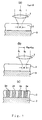
- molding tools are manufactured using a glass substrate 3 that is polished with the precision of an optical surface. After the substrate 3 is cleaned, it is coated with a primer, for example, a silane-coupling agent. A photoresist 2 is then applied by spin coating and subjected to a pre-bake process. Positive-type, i.e. , wherein the region exposed to light is removed during development, photoresist 2 is often used. The reason is that the surface roughness can be made smaller by the positive-type photoresist, so that to obtain lower noise is advantageous. Accordingly, following explanations are to be assumed to use a positive-type photoresist.
- a laser beam recorder or a laser cutting machine is used to expose the photoresist 2 [ sic ] with a pattern of pits and/or grooves where the width of pits and grooves is generally determined by the laser spot diameter.
- the laser beam is converged to the diffraction limit by the lens 1.
- the depth of the pits and grooves is generally determined by the thickness of the photoresist 2.
- the photoresist 2 is illuminated by a predetermined exposure light along the first line O 1 via the lens 1 (Fig. 9(a)).
- the illumination is continuous while forming grooves and is intermittent while forming pits.
- the illuminated area (exposed area) becomes the first groove of the molding substrate afterward.
- the spot diameter of the exposure light directly defines the line width of the 'exposed area' (hereinafter, the 'exposed area' may be abbreviated to the 'exposure area').
- the minimum spot diameter is defined by the diffraction limit of the exposure light and it depends the wavelength ⁇ of the exposure light.
- the light intensity distribution in the light beam shows the Gaussian distribution, so that the intensity is the strongest at the center and becomes weaker in the periphery. Therefore, the effective spot diameter (diameter of the removed area of the exposed photoresist by development) becomes smaller than the value defined by diffraction limit according to the sensitivity of the photoresist or the developing condition.
- the effective diameter becomes further narrower.
- the value ⁇ has defined the groove width of the resist pattern and, accordingly, the groove width Gw of the molding substrate.
- ⁇ denotes the effective spot diameter.
- the groove width Gw When the groove width Gw is necessary to be large, it can be performed such that the spot diameter may not be narrowed up to diffraction limit or that the exposure light is used in the state of out of focus.
- the predetermined line width cannot be obtained by one exposure, another exposure parallel to the first exposure can be performed repeatedly after moving the illuminating position by a necessary amount.
- the illuminating position is moved from the first line to the second line O 2 separated by the distance corresponding to the sum of the groove width Gw and the land width Lw (which is parallel to the first line) (Fig. 9(b)).
- the photoresist On moving the exposure light along the second line O 2 , the photoresist is illuminated (exposed). Generally, this process is repeated a plurality of times regarding the second line O 2 as the first line O 1 . Accordingly, a plurality of the exposure areas 2e of concentric circular rings are obtained (Fig. 9(c)).
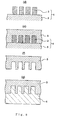
- a resist pattern having grooves and pits on the substrate surface is obtained by developing the exposed photoresist. Following development, the resist pattern may optionally undergo a 20-60 minute post-bake at 80-120°C. When such a post-bake is used, the resist pattern is then cooled down to room temperature. This is shown in Fig. 10(d).
- the resist pattern in combination with the substrate 3 shown in Fig. 10(d) is called the master substrate or master 4.
- the master substrate 4 is equivalent to the replica 46 in Fig. 4 of Hunyar U.S. Patent No. 4,211,617.
- the master substrate 4 undergoes metallization treatment to form a conductive layer on the surface. Generally such treatment is carried out by sputtering (dry-type method), or by non-electrolytic plating (wet-type method). Following metallization, a thick plating layer, such as nickel (Ni), is formed upon the master substrate 4 by an electroforming method.
- a thick plating layer such as nickel (Ni)
- Ni nickel
- the double layer structure that consists of a conductive layer and the Ni plating layer is referred to as the 'father stamper' or just the 'father' (in this specification and claims, referred as the 'stamper'). This is shown in Fig. 10(e).
- a free stamper 5 is obtained when the stamper 5 is peeled from the master substrate 4. This is indicated in Fig. 10(f).
- the stamper 5 is equivalent to mother member 52 in Fig. 6 of Hunyar U.S. Patent No. 4,211,617.
- stamper 5 is generally thin, approximately 200-300 ⁇ m in thickness. After peeling, the stamper 5 undergoes solvent treatment, such as acetone or the like, to remove resist since a portion of the resist may remain on the stamper 5. Resist must be removed since the concavities and protuberances on the surface of the stamper would otherwise be destroyed. Only a single stamper 5 is obtained from a single master substrate 4 since the resist pattern 2 is damaged during peeling. The obtained stamper 5 has an extremely precise pattern of concavities-protuberances. Actually, since the stamper 5 after peeling has a rather inaccurate dimension, a central hole is bored in the center of the stamper 5, and the unused portion of the outside perimeter is cut off. Before the processing the concavity-protuberance surface (signal surface) is shielded with a protective coat. Thus, an annular shaped stamper 5 is obtained.
- the molding substrate is formed by using the stamper 5.
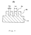
- Soft resin (or liquid resin) 6 is pressed against the stamper 5. This is shown in Fig. 10(g). Accordingly, the concavities-protuberances of the stamper 5 are embossed on the resin.
- the hardened or cured resin 6 is peeled away from the stamper 5 to form the molding substrate 6 shown in Fig. 11(h).
- the molding substrate 6 has the concavities-protuberances formed by grooves having the width Gw and lands having the width Lw lined in turn.
- a pressure molding or an injection molding can be used. Generally, the injection molding is used because of its high productivity.
- the light source having shorter wavelength than argon laser cannot be available so far because there has been neither appropriate laser having shorter wavelength with continuous oscillation nor photoresist which has sensitivity to the short wavelength ⁇ (ultraviolet light) and which makes it possible to etch groove walls vertically. Accordingly, the groove width Gw has had the shortest value of about 0.23 ⁇ m so far. However, the request for increasing recording density has become stronger, and the technique capable of forming a finer groove width Gw has been expected.
- An invention according to claim 1 is a method for manufacturing a master substrate for producing a grooved molding substrate comprising steps of a preparing step that prepares a substrate on which a photoresist is coated, an exposing step that exposes the photoresist to a light with a predetermined pattern such that the exposed part becomes a land of the grooved molding substrate, and an obtaining step that obtains the master substrate by developing the photoresist.
- a replica is formed by using the master substrate, and a stamper is manufactured by using the replica.
- the stamper is manufactured directly from the master substrate.
- a molding substrate is manufactured by using either one of these stampers. Therefore, in the master substrate according to the present invention, a photoresist area (exposed area) where a pattern is exposed becomes an area corresponding to the land (not groove) in the molding substrate which is final product, which is different from the prior art. Accordingly, what is defined by the wavelength of the exposure light is the land width Lw.
- the groove width Gw is defined by the separation between the adjacent exposed areas.
- the master substrate is manufactured by suitably arranging the separation between the adjacent exposed areas.
- the master substrate By using the master substrate, a narrow-grooved molding substrate that has been impossible can be manufactured. (In the present invention, the remaining photoresist after development forms the protuberant portion, and the area where the removed photoresist was forms the concave portion in the master substrate. When the photoresist is removed all the way in the thickness direction, the groove depth formed in the grooved molding substrate is correspondent to the thickness of the photoresist.)
- An invention according to claim 2 is a method for manufacturing a master substrate for producing a grooved molding substrate comprising steps of a preparing step that prepares a substrate on which a photoresist is coated, an exposing step that exposes the photoresist to a light with a predetermined pattern such that the exposed part becomes a land of the grooved molding substrate, an acquiring step that acquires a resist pattern by developing the photoresist, an etching step that etches a part of the substrate not covered by the photoresist, and an obtaining step that obtains the master substrate by removing the photoresist.
- This invention also has the same effect as the invention according to claim 1.
- a master substrate that can be used repeatedly is obtained by suitably choosing the material of the substrate.
- the groove depth can be controlled by the etching depth, a deep groove that has been impossible to manufacture can be manufactured, and a groove having a steep sidewall and a smooth bottom surface can be also manufactured.
- An invention according to claim 3 is a method for manufacturing a master substrate for producing a grooved molding substrate comprising steps of a first step that prepares a substrate on which a photoresist is coated, a second step that forms a part corresponding to a first land of the grooved molding substrate by illuminating and exposing the photoresist along a first line with a predetermined exposing light, a third step that moves the illuminating position from the first line to a second line apart from a distance Corresponding to a summation of a groove width Gw and a land width Lw of the grooved molding substrate, a fourth step that forms a part corresponding to a second land of the grooved molding substrate by illuminating and exposing the photoresist along the second line with the exposing light, and a fifth step that obtains the master substrate by developing the photoresist, or instead of the second through fourth steps, a step that forms a part corresponding to a spiral shaped land of a grooved molding substrate by il
- a narrow-grooved molding substrate that has been impossible can be manufactured because of the same reason as described in the invention according to claim 1.
- the remaining photoresist after development forms the protuberant portion, and the area where the removed photoresist was forms the concave portion in the master substrate.
- the groove depth formed in the grooved molding substrate is correspondent to the thickness of the photoresist.
- an invention that has the second through fourth steps is used for manufacturing a grooved molding substrate having a pattern of concentric circular rings.
- an invention having, instead of the second through fourth steps, a step that forms part corresponding to a spiral shaped land of a grooved molding substrate by illuminating and exposing along a spiral line having an interval corresponding to a distance corresponding to a summation of a groove width Gw and a land width Lw of the grooved molding substrate is used for manufacturing a grooved molding substrate having a spiral pattern. It is needless to say that either invention has the first and fifth steps.
- the exposure separation is apart from a distance corresponding to a summation of a groove width Gw and a land width Lw of the grooved molding substrate.
- the land width Lw is defined by the exposure condition. Accordingly, although the groove width becomes the exposure separation subtracted by this land width Lw, the groove width Gw, which is a target, is obtained because the exposure separation is set as described above. Since the groove width Gw is not defined by the exposure condition, the groove width can be less than the effective spot diameter ⁇ .
- An invention according to claim 8 is a method for manufacturing a master substrate for producing a grooved molding substrate comprising steps of a first step that prepares a substrate on which a photoresist is coated, a second step that forms a part corresponding to a first land of the grooved molding substrate by illuminating and exposing the photoresist along a first line with a predetermined exposing light, a third step that moves the illuminating position from the first line to a second line apart from a distance corresponding to a summation of a groove width Gw and a land width Lw of the grooved molding substrate, a fourth step that forms a part corresponding to a second land of the grooved molding substrate by illuminating and exposing the photoresist along the second line with the exposing light, a fifth step that obtains a resist pattern by developing the photoresist, a fifth (a) step that etches a part of the substrate not covered by the photoresist, and a fifth (b) step that obtains
- the difference from the invention according to claim 3 is that although the invention according to claim 3 uses concavity-protuberance of the developed resist pattern as that of the master substrate, the present invention uses the etched portion as the concave portion, and the remaining portion as the protuberant portion, which is the same invention as claim 2.
- the groove depth of the grooved molding substrate formed by using the master substrate manufactured by the method according to the present invention becomes the etching depth.
- This invention also has the same effect as the invention according to claim 3.
- the groove depth can be controlled by the etching depth, and a groove having a steep sidewall and a smooth bottom surface can be also manufactured. Accordingly, when the substrate is used for a medium, a grooved molding substrate having low noise can be obtained. Moreover, this master substrate can be used repeatedly.
- inventions according to claims 4 and 9 are the inventions according to claims 3 and 8, respectively, wherein after finishing the fourth step and before starting the fifth step, a combination of the third and fourth steps is carried out a plurality of times by regarding the second line in the fourth step as the first line in the third step.
- a master substrate for manufacturing a grooved molding substrate having a plurality of grooves for example, concentric circular rings or parallel stripes can be manufactured.
- inventions according to claims 5 and 10 are the inventions according to claims 3 and 8, respectively, wherein the groove width Gw is 0.1 ⁇ m or less.
- the recording density can be greatly increased relative to the conventional grooved molding substrate.
- inventions according to claims 6 and 11 are the inventions according to claims 3 and 8, respectively, wherein the groove width Gw is 0.06 ⁇ m or less.
- the recording density can be further greatly increased relative to the conventional grooved molding substrate.
- inventions according to claims 7 and 12 are the inventions according to claims 3 and 8, respectively, wherein the groove of the grooved molding substrate is a hollow, a pit, or discontinuous.
- the groove of the grooved molding substrate is a hollow, a pit or discontinuous, in a grooved molding substrate formed by using the master substrate manufactured in accordance with the present invention, the groove becomes a hollow, a pit, or discontinuous. Accordingly, the arrangement of those can be used as binary information.
- An invention according to claim 13 is a method for manufacturing a stamper comprising steps of a sixth step that, after obtaining the master substrate manufactured by the method for manufacturing a master substrate for producing a grooved molding substrate according to any one of claim 1 through 12 by using a positive type photoresist as a photoresist, manufactures a replica from the master substrate, and a seventh step that manufactures the stamper from the replica by using an electroforming method.
- any one of claim 1 through 12 when a positive type photoresist is used, the exposed area becomes a concave portion of the resist pattern. Therefore, when a stamper is directly manufactured from the master substrate by using electroforming method, the exposed area becomes the groove of the grooved molding substrate, which is just the same as the prior art. Accordingly, in order to reverse concavities-protuberances, a replica is formed from the master substrate, and a stamper is manufactured from the replica by using electroforming method. Using the electroforming method, an accurate stamper having a fine surface roughness can be easily manufactured.
- An invention according to claim 14 is the invention according to claim 13, wherein the replica is made from metal or resin.
- the replica When metal is used for the replica, the replica is manufactured from the master substrate by using electroforming method.
- resin When resin is used for the replica, the replica is manufactured by curing after ductile resin is pressed against the master substrate, and is duplicated. In either case, an accurate replica having a fine surface roughness can be manufactured.
- it is more preferable to use resin because the replica can be obtained more easily and, moreover, when concavities-protuberances is formed on the master substrate by etching such as the invention according to claim 2 or 8, the master substrate can be used repeatedly.
- An invention according to claim 15 is a method for manufacturing a stamper for producing a grooved molding substrate comprising a sixth step that, after obtaining the master substrate manufactured by a method for manufacturing a master substrate for producing a grooved molding substrate according to any one of claim 1 through 12 by using a negative type photoresist as a photoresist, manufactures the stamper from the master substrate by using an electroforming method.
- any one of claim 1 through 12 when a positive type photoresist is used, the exposed area becomes a concave portion of the resist pattern. Therefore, when a stamper is directly manufactured from the master substrate by using electroforming method, the exposed area becomes the land of the grooved molding substrate. Accordingly, a stamper is directly manufactured from the master substrate by using electroforming method contrary to the invention according to claim 13. Using the electroforming method, an accurate stamper having a small surface roughness can be easily manufactured.
- An invention according to claim 16 is a method for manufacturing a stamper comprising steps of a preparing step that prepares a substrate on which a photoresist is coated, an exposing step that exposes the photoresist to a light with a predetermined pattern, an acquiring step that acquires a resist pattern by developing the photoresist, an etching step that etches a part of the substrate not covered by the photoresist, an obtaining step that obtains a master substrate by removing the photoresist, a forming step that forms, a resin replica from the master substrate, and a manufacturing step that manufactures the stamper from the replica by using an electroforming method.
- the material can be chosen from durable materials.
- the etching depth can be controlled, the groove depth of the grooved molding substrate can be controlled.
- a grooved molding substrate having a small surface roughness can be manufactured.
- the number of times for using the master substrate can be extended. Since the electroforming method is used for manufacturing the stamper from the replica, an accurate stamper having a small surface roughness can be easily manufactured.
- a resin replica can be used repeatedly, and can manufacture any number of stampers.
- inventions according to claims 17 and 18 are methods for manufacturing a grooved molding substrate comprising steps that, after obtaining stampers manufactured by the inventions according to claims 13 and 15, respectively, manufacture a grooved molding substrate by forming glass or resin with each stamper.
- a grooved molding substrate whose groove is correspondent with an unexposed area of the master substrate. Accordingly, a grooved molding substrate whose groove width is narrower than the effective spot diameter ⁇ defined by the wavelength of the exposure light can be obtained.
- An invention according to claim 19 is a grooved molding substrate manufactured by an injection molding method by using a stamper, wherein the groove width Gw is 0.1 ⁇ m or less.
- the recording density can be greatly increased relative to the conventional grooved molding substrate.
- An invention according to claim 20 is the invention according to claim 19, wherein the groove width Gw is 0.06 ⁇ m or less.
- the recording density can be further greatly increased relative to the conventional grooved molding substrate.
- An invention according to claim 21 is the invention according to claim 19, wherein the sloping angle of the sidewall of the groove is 85° or more.
- the sloping angle of the sidewall of the groove is 85° or more, noise is reduced, optical cross-talk between adjacent tracks is lowered, and thermal cross-talk (cross erasure) is reduced. Moreover, the wobble signal is accurately reproduced, CNR improves, and dropout of the various read-write signals becomes extremely low.
- An invention according to claim 22 is the invention according to claim 19, wherein the ratio of the groove depth d to the groove width Gw is 0.1 or more.
- An invention according to claim 23 is the invention according to claim 19, wherein the groove is a pit or discontinuous.
- the arrangement of pits, or discontinuous grooves can be used as binary information.
- Inventions according to claims 24, 25 and 26 are memory media whose substrates are manufactured by the method for manufacturing a grooved molding substrate according to claim 17 and 18, respectively, and a substrate according to claim 19.
- the memory medium means a medium on which information can be recorded, such as optical disks, magneto-optical disks, hard disks, and the likes.
- a hard disk having a high recording density and a high S/N ratio can be obtained.
- the land is generally used for recording and the groove is generally used for tracking, so that the groove may be narrow although the land need to have a certain width.
- the groove width can be narrower than this, so that recording density can be higher for that.
- inventions according to claims 27, 28 and 29 are memory devices having the memory media according to claims 24, 25, and 26, respectively.
- inventions according to claims 30, 31 and 32 are computers having the memory devices according to claims 27, 28, and 29, respectively.
- a memory device having the same memory capacity can be small, or a memory device having the same dimension can be made to have more memory
- grooves may be pits, hollows, or discontinuous dints.
- a molding substrate having the lowest groove width Gw of 0.02 ⁇ m, or 0.01 ⁇ m according to circumstances can be manufactured.
- a special feature of the present invention is to make it possible to manufacture a groove having a width smaller than 0.23 ⁇ m which has been unable.
- the groove width is preferably 0.01 ⁇ m to 0.23 ⁇ m, more preferably 0.02 ⁇ m to 0.1 ⁇ m, and furthermore preferably 0.03 ⁇ m to 0.08 ⁇ m.
- the groove depth of 1 nm to 1 ⁇ m.
- the substrate 3 is prepared.
- the substrate 3 is usually disk shaped, it is possible for the substrate 3 to, be polygonal, not limited to the disk shape.
- the substrate 3 material mainly include glass materials. Suitable glass materials include soda lime glass (green plate glass), aluminosilicate glass (white plate glass), alkali-free glass, low-expansion glass, crystalline glass and ceramic materials. Quartz, for example, fused quartz or synthetic quartz, or even Si can be used as the ceramic material. Additionally, if desired, it is possible for the substrate 3 to use a metal substrate material, such as, Al, Fe, Cu, etc.
- the substrate 3 surface is precisely polished in order to obtain a highly precision surface. It is also permissible to form a surface layer upon the substrate surface.
- suitable surface layer materials include:
- the surface is coated with a photoresist 2.
- a photoresist may be applied by spin coating.
- a primer such as a silane coupling agent coating, is applied to the substrate prior to photoresist coating. This primer improves adhesion of the photoresist 2 to the substrate 3.
- a primer is not needed such as when Cr, TiN, etc. exist in the surface layer.
- the photoresist depth determines the depth of pits and grooves. In the case of the master substrate II, the etching time determines the depth of grooves.
- a low temperature pre-bake may be carried out to adjust resist sensitivity.
- a laser beam recorder is used to illuminate the resist according to a prescribed pattern of pits, grooves, etc. The resist 2 is exposed in this manner.
- the photoresist 2 is illuminated by the predetermined exposure light along the circular first line (O 1 ) with the effective spot diameter ⁇ via the lens 1 (Fig. 1(a)). This corresponds to a second step.
- the illuminated area (exposed area) becomes a first land (groove in the prior art) of the molding substrate afterward.
- ⁇ denotes the aforementioned effective spot diameter and, in this case, becomes equal to the land width Lw.
- the illumination position is moved from the first line O 1 to the circular second line O 2 separated by the distance corresponding to the summation of the groove width Gw and the land width Lw of the grooved molding substrate (Fig. 1(b)). This corresponds to a third step.
- the photoresist 2 is illuminated (a fourth step). Now, the exposure to a portion corresponding to a second land has completed.
- the third step in combination with the fourth step is repeated a plurality of times regarding the second line in the fourth step as the first line in the third step. Accordingly, the photoresist 2 is exposed along a plurality of concentric circular rings. The state where the exposure has completed is shown in Fig. 1(c). The exposed area is denoted by 2e.
- the repetition of the third and fourth steps is for forming lands and grooves in a pattern of concentric circular rings, when a spiral shape is to be formed, the illumination may be performed along a spiral shape to be aimed instead of the repetition of the third and fourth steps.
- the exposed resist 2 is immersed in developing solution, and the resist is developed.
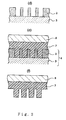
- the developing solution include solutions of inorganic alkaline compounds such as sodium phosphate, calcium phosphate, sodium hydroxide, calcium hydroxide, etc. It is also possible to use an organic, rather than inorganic, alkaline solution. Since a positive type photoresist 2 is used, the exposed area 2e dissolves in the developing solution. Having dissolved the photoresist, resist is washed with ultrapure water and the underlying substrate 3 is exposed within the dissolved portions. A substrate 3 obtained in this manner that has a photoresist 2 patterned on its surface. This is shown in Fig. 2(d). This type of photoresist pattern 2, together with the substrate 3 or pattern alone, is referred to as the "resist pattern.” Such a resist pattern is referred to as the master substrate I (4).
- the photoresist 2 After development, it is possible to heat the master substrate I (4) to a somewhat high temperature during a post-bake. A post-bake is sometimes used to increase the sidewall angles of grooves and pits. Post-baking can also be used to improve resistance of the resist to etching, to improve adhesion between the resist 2 and the substrate 3 and also to harden the resist surface. By increasing the photoresist's hardness, the photoresist 2 is able to endure subsequent processes, including metallization and the formation of a plating layer upon the conductive layer by the electroforming method.
- the master substrate I (4) is prepared.
- the exposed portion of the resist 2 is dissolved and the substrate 3 is exposed within a portion of this resist, the exposed region is etched so as to provide a concave region upon the substrate 3 (the fifth (a) step).
- This concave pattern is identical to the resist 2 pattern.
- the depth of the concave region is defined by the etching time.
- the dry process is preferred for etching although it is possible to utilize the wet process. Among dry processes, the reactive ion etching (RIE) method is particularly advantageous.
- Other etching processes that can be used include etching utilizing magnetron RIE, electron cyclotron resonance (ECR), induction-coupled plasma (ICP), helicon waves, etc.
- RIE reactive ion ion ion ion ion ion ion ion ion ion ion ion ion ion ion ion ion ion ion ion ion ion ion ion ion ion ion ion ion ion ion ion ion ion ion ion .
- a high plasma density process greater than 10 11 ions/cm 3
- the latter includes RIE utilizing ICP or helicon waves that are advantageous for use with particularly fine patterns.
- etching a substrate 3 that has a surface layer is advantageous since it becomes possible to carry out etching uniformly.
- the surface layer thickness determines the depth of the grooves, etc.
- the remnant resist is removed after the etching process (the fifth (b) step). Removal may be carried out by a dry etching process (ashing) using oxygen plasma. Alternatively, the remnant resist is removed by immersion in a heated container holding a concentrated acidic solution such as concentrated sulfic acid or concentrated nitric acid. Addition of hydrogen peroxide to such a solution improves resist removal. After resist is removed in this manner, the substrate surface is washed, for example, with ultrapure water.
- a ceramic substrate is obtained that has protuberances corresponding to the pits and grooves shown in Fig. 8(a).
- the substrate becomes the master substrate II (4B) according to the present invention.
- Ceramic material is particularly preferred as a material of construction of this substrate. Ceramic material is preferred since the ceramic surface is quite smooth. In other words, ceramic material surface roughness (Ra) is extremely low (Ra ⁇ 10 nm or Ra ⁇ 1 nm according to circumstances). Optical disk noise is reduced when such a ceramic material is used for the manufacture of optical disks. Therefore the superiority of ceramic material is acknowledged by calling a master substrate II (4B) a "ceramic mold" in the specification.
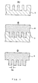
- a replica is modeled upon the master substrate and has concavities-protuberances reversed from the master substrate.
- the material of the replica may be metal or resin.
- a metallic replica is manufactured by electroforming on the master substrate. This method is the same method for manufacturing a stamper described later.
- resin is preferable for the material of a replica. Particularly resin is preferable when the master substrate I is used because a resin replica makes it possible to use the master substrate I repeatedly. Thus, a resin replica is explained below.
- a master substrate 4 (master substrate I or II) is provided.
- Soft resin 7 is pressed against the concavity-protuberance surface (signal surface) of the master substrate 4. Then, the resin 7 is hardened or cured as shown in Fig. 2(e). The hardened or cured resin 7 is a copy of the concavities-protuberances of the master substrate. The resin 7 is then peeled away from the master substrate to form a replica.
- the resin 7 provides superior duplication performance when pressed against the master substrate.
- Resins with low viscosity or high fluidity generally have good duplication performance.
- Typical method for lowering viscosity involve (a) heating and softening the resin. In this case, the resin 7 is subsequently cooled and hardened.
- the resin 7 may be mixed with a solvent. In this case, the resin 7 hardens after the solvent is volatilized.
- a preferred method (c) employs a low viscosity material such as a low molecular weight resin, prepolymer, or resin raw material. Additionally, while not performed, such a material can be liquid. When the master substrate I is used for the resist pattern, it is preferable to use liquid type resin.
- the method (c) is the most preferable.
- the way to promote polymerization in the method (c) is heating or radiation exposure.
- two resin liquids may be mixed together, and the resin mixture is allowed to simply react and polymerize.
- Ion beam radiation, electron beam radiation, ultraviolet radiation, far ultraviolet radiation, laser light, x-rays, synchrotron radiation, etc. are examples of the types of radiation that may be used. Ultraviolet radiation, however, is preferred due to ease of handling.
- the master substrate 4 is placed with the concavity-protuberance surface facing upward while a low-viscosity ultraviolet-curing resin liquid 7 is poured slowly from above.
- a transparent plate 8 such as a glass plate, may be placed upon the resin liquid so as to avoid the introduction of bubbles. Ultraviolet radiation may be applied through the transparent plate 8, thereby causing the resin to cure.
- the cured resin 7, together with the transparent plate 8, is peeled from the master substrate 4.
- a replica 7 is obtained in this manner that consists of two layers: cured resin 7 and transparent plate 8.
- a suitable transparent plate 8 may be a glass plate of at least 0.6 mm thickness, preferably about 4 mm to about 10 mm thick.
- the glass plate should have a surface roughness that is low in comparison to the substrate 3 of the master substrate.
- a good surface roughness (Ra) value for the glass plate is 5 nm to 1 ⁇ m.
- resin materials such as, polycarbonate, polystyrene, polyolefins, acrylic resins, etc., rather than glass plate.
- a primer such as a silane coupling agent
- the primer is heated (baked) after it is applied.
- silane coupling agents which may be used as the primer include vinyl silanes, acrylsilanes, epoxy silanes, aminosilanes, etc.
- vinyl silanes include, vinyltrichlorosilane, vinyltris( ⁇ -methoxyethoxy) silane, vinyltriethoxysilane, vinyltrimethoxysilane, etc.
- Examples of acrylsilanes include ⁇ -methacryloxypropyltrimethoxysilane, etc.
- examples of epoxy silanes include ⁇ -(3,4-epoxycyclohexyl)ethyltrimethoxysilane, ⁇ -glycidoxypropyltrimethoxysilane, ⁇ -glycidoxypropylmethyldiethoxysilane, etc.
- aminosilanes includes N- ⁇ -(aminoethyl)- ⁇ -aminopropyltrimethoxysilane, N- ⁇ -(aminoethyl)- ⁇ -aminopropylmethyldimethoxysilane, ⁇ -aminopropyltriethoxysilane, N-phenyl- ⁇ -aminopropyltrimethoxysilane, etc.
- silane coupling agents include ⁇ -mercaptopropyltrimethoxysilane, ⁇ -chloropropyltrimethoxysilane, etc.
- primers examples include silanes, such as, chlorosilanes and alkoxysilanes, silazanes, or special silylating agents. It is also possible to mix two or more of these primers.
- the primer can be used as a dilute solution in a solvent such as toluene, xylene, ethanol, methanol, isopropanol, etc.
- the resin of the replica examples are listed below. Generally, the resin can be classified as either (A) thermoplastic resins or (B) thermosetting resins.
- thermoplastic resins include polycarbonates, polystyrenes, styrene-type polymer alloys, polyolefins, polypropylenes, amorphous polyolefins, acrylate resins (such as polymethacrylates), polyvinylchlorides, thermoplastic polyurethanes, polyesters, nylons, etc.
- thermosetting resins include, but are not limited to, thermosetting polyurethanes, epoxy resins, unsaturated acrylate resins, etc.
- a preferred example is a curing resin solution mainly composed of urethanated poly(meth)acrylate, polycarbonate di(meth)acrylate, and acetalglycoldiacrylate.
- thermosetting resin When a thermosetting resin is used, a low molecular weight resin liquid is made to contact the master substrate.
- This resin solution can contain a curing catalyst or a curing agent.
- the curing catalyst is a photosensitizer when curing takes place due to ultraviolet radiation exposure.
- photosensitizers which may be used include acetophenones, benzoin alkyl ethers, propiophenones, ketones, anthraquinones, thioxanthones, etc. It is also possible to use various types of photosinsitizers mixed together. In particular, 1-hydroxycyclohexyl phenyl ketone, etc.
- Ketone-type photosensitizers are preferred due to their good duplication performance, mold releasability, and stability. Resins that cure upon exposure to ultraviolet light are called “ultraviolet curable resin” and are preferred for use as the resin of the stamper. Indeed, it is preferred that the resin does not adhere to the stamper, particularly during peeling away from the resin replica in a later process.
- the color number (APHA) is 30-50,and refractive index at 25°C is 1.4-1.8. It is preferable for duplicating performance that specific gravity and viscosity of resin solution at 25°C are 0.8-1.3 and 10-4800 CPS, respectively.
- an anti-static agent In order to counter static electricity during the last electroforming process or ion plating process, it is possible to mix an anti-static agent into the resin liquid. Alternatively, a thin anti-static layer (such as a Pt layer) is formed after the replica is completed. This type of anti-static treatment prevents problems such as burning, deformation, peeling, contaminant attachment, etc.
- the skin of the peeled resin replica from the master substrate 4 has generally small surface roughness Ra.
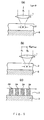
- the stamper 5 is manufactured by plating the replica 7 using either a thick or a thin layer method as shown in Fig. 3.
- the plating layer becomes the stamper 4.
- dry and wet plating methods there are non-electrolytic plating and electrolytic plating.
- the dry method is called "vacuum layer deposition.” Technologies for vacuum layer deposition include vacuum metallization, ion plating, sputtering, etc.
- Primary methods include dry plating and non-electrolytic plating.
- the second method is electrolytic plating. Plating may be carried out by a primary method or a secondary method.
- Electrolytic plating can form a thick plating layer during a short time period.
- a thin, generally about 30-100 nm, metal layer is formed upon the replica [ sic ]. This metal layer is called “conductive layer” and this process is called “metallization.”
- Metallization is generally carried out by a primary method.
- Ni nickel
- other suitable metals which may be used include Au, Pt, Pd, Ag, Ti, Ta, Cr, etc.
- Au gold
- Pt palladium
- Pd silver
- Ti titanium
- Ta titanium
- Cr nickel
- a metal that contains phosphorous Particularly when Ni is used as the metal, it is possible to first form a primer layer consisting of another metal or metal containing compound that has a thermal expansion coefficient nearly the same or equivalent to that of Ni itself. The conductive layer is formed upon this primer. During or after electroforming, this primer layer can decrease the strain resulting from electroforming layer stress. This strain phenomenon can sometimes destroy the pit and groove, etc., concavities. This primer layer may be removed after the stamper 5 is completed.
- the resin replica with the conductive layer is immersed in a plating solution in order to carry out electroforming.
- a nickel sulfamate solution is used as this plating solution.
- a Ni plating layer is formed upon the conductive layer as electroforming is carried out.
- This Ni plating layer is the stamper 5.
- metals other than Ni Alternatively, it is possible to mix other metals, i.e., Ti or elements, i.e., P with the Ni. Mixture with P can result in a mold with a great surface hardness. It is possible to obtain a hard stamper with a ling working life by the use of a Ni-P, Ti-P, or Ni-Ti-P, etc. alloy composition for the conductive layer, plating layer, or both the conductive layer and plating layer.
- Ni plating layer it is possible, instead of a simple Ni plating layer, to add other plating layers, for example, metals such as silver, copper, or chrome, or alloys of such materials, to the Ni plating layer.
- plating layers for example, metals such as silver, copper, or chrome, or alloys of such materials, to the Ni plating layer.
- the stamper 5 can also be manufactured by dry plating or non-electrolytic plating without the use of electroforming.
- the dry method avoids the problem of waste water treatment.
- ion plating is capable of providing a stamper that has particularly low surface roughness.
- Concavities-protuberances of the stamper disappear as the deposited plating layer thickness exceeds about 100 ⁇ m. That is to say, the plating layer surface appears flat. Generally, plating stops when the plating layer thickness reaches about 200 to about 600 ⁇ m thick, preferably, about 250 ⁇ m to about 300 ⁇ m. The stamper 5 is then completed.
- the stamper 5 is still attached to the replica 7, so that the stamper is then peeled away from the replica 7. This peeling must be carried out carefully since the stamper 5 is a thin metal membrane (generally 250-300 ⁇ m thick).
- the peeled stamper 5 has a clean concavity-protuberance surface (shown in Fig. 4(h)). Although it does not basically need to be cleaned, the stamper 5 may be cleaned. Washing treatment typically involves either wet washing using organic solvent or purified water, or dry washing such as ashing, plasma treatment, ultraviolet exposure, ozone cleaning, etc.
- the back surface of the stamper may be mechanically polished.
- the concavity-protuberance surface (information surface) of the stamper 5 is given a protective coating in order to protect the stamper's concavity-protuberance surface.
- This protective coating is formed by applying a peelable protective coating, followed by drying.
- the stamper 5 is peeled from the replica 7, polished its back surface, and then a hole is mechanically drilled in the vicinity of the center.
- the outer perimeter of the stamper 5 is removed in a similar manner. This results in a finished annulus-shaped stamper. Shipment of the stamper is then possible.
- Surface roughness Ra of the stamper is generally smaller than 10 nm. In most case, a stamper is having surface roughness smaller than 1 nm. When a master substrate II is produced using the RIE method, the resultant stamper has little surface roughness. Thus it is possible to manufacture a particularly high quality stamper.
- a grooved molding substrate is manufactured by using the method for forming a copy of the concavities-protuberances surface of the stamper (Fig. 4(i)).
- a grooved molding substrate 6 having smaller groove width Gw than the effective spot diameter ⁇ is obtained.
- the formed grooved molding substrate 6 is shown in Fig. 4(j).
- Methods for manufacturing grooved molding substrate include injection, pressing, casting, etc. The injection molding method has the highest productivity among such molding methods.
- the resin used for the grooved molding substrate is generally a thermoplastic resin, particularly a relatively hard resin.
- resins include, polycarbonates, polystyrenes, styrene-type polymer alloys, acrylate resins (such as polymethacrylates), polyvinylchlorides, polyesters, nylons, ethylenevinylacetate resins, amorphous polyolefins, etc.
- thermosetting resins include epoxy resins, thermosetting polyurethanes, unsaturated acrylate resins, unsaturated polyesters, diethyleneglycol-bis-allylcarbonate resins, etc. Glass materials having a low melting point can be used instead of resins.
- the molding technology of the grooved molding substrate is just same as prior art, so that the explanation is left out.
- the substrate 3 coated with the negative type photoresist 2 is prepared. Since the following explanation is basically same when the positive type photoresist is used as described above, the explanation is brief.
- the illumination position is moved from the first line O 1 to the circular second line O 2 separated by the distance corresponding to the summation of the groove width Gw and the land width Lw (Fig. 5(b)). This corresponds to a third step.
- the photoresist 2 is illuminated (a fourth step).
- the third step in combination with the fourth step is repeated a plurality of times regarding the second line in the fourth step as the first line in the third step. Accordingly, the photoresist 2 is exposed along a plurality of concentric circular rings. The state where the exposure has completed is shown in Fig. 5(c). The exposed area is denoted by 2e. The unexposed area corresponds to grooves.
- the repetition of the third and fourth steps is for forming lands and grooves in a pattern of concentric circular rings, when a spiral shape is to be formed, the illumination may be performed along a spiral shape to be aimed instead of the repetition of the third and fourth steps.
- the exposed resist 2 is developed. Since a negative type photoresist 2 is used, the exposed area 2e remains, and the unexposed area dissolves in the developing solution. A photoresist pattern 2 shown in Fig. 6(d) is obtained and, thus, a master substrate I (4) consisting of the pattern 2 and the substrate 3 is obtained.
- the master substrate I(4) shown in Fig. 6(d) is prepared. Then, the master substrate II (4B) shown in Fig. 8(b) is manufactured by etching, and then removing residual resist as described before when the master substrate II is manufactured by using a positive type photoresist.
- the stamper 5 is manufactured by plating the master substrate 4 (although the master substrate II can be used, the master substrate I is used in the figure).
- the plating layer becomes the stamper 5.
- a free stamper 5 as shown in Fig. 6(f) is obtained by peeling the stamper 5 from the master substrate 4.
- a grooved molding substrate 6 having grooves 6a and lands 6b is formed from resin or glass materials by injection molding (resin) or pressing molding (glass) using aforementioned stamper 5.
- the explanation of the method is left out because it is just the same as when the positive type photoresist is used.
- Fig. 12 is a schematic showing a hard disk.
- a magnetic layer 22 [ sic ] is formed on the substrate 21 having lands and grooves.
- the molding substrate according to the present invention can be used for the substrate 21 of the hard disk.
- the material for the substrate is preferably resins or glasses, and particularly low-melting glass is preferable.
- the substrate 21 has a spiral shaped groove or fine grooves in a pattern of concentric circular rings.
- the magnetic layer 22 is made from CoCr, CoCrPt, CoCrTa, and/or the like deposited by sputtering. According to circumstances, a protective layer and an under layer are formed upon and under the magnetic layer, respectively.
- the lands have to have a certain amount of width.
- the width has to be about the same or wider than that defined by the exposure optical system.
- grooves may be narrow. Therefore, the recording density can be increased by using the substrate according to the present invention for the substrate 21.
- a hard disk drive is composed of a data input terminal 31, a data processing circuit 34 for processing data passing through the terminal, a data recording/regenerating circuit 35 for converting the data processed the circuit 34 into recording data, transmitting to a head (without sign), and converting the data regenerated by the head into regenerating signal, a hard disk 36 on which the data is recorded data through the head, a motor 39 for driving the hard disk, a servo system control circuit 38 for controlling the motor, a control data input/output terminal 32, a control data processing circuit 37 for processing data input/output from the terminal 32, and a central processing circuit CPU 33 for controlling the circuit 34, 37, and 38, and for performing various calculation.
- the data recorded on the hard disk 36 is regenerated through the head and transmitted to the data recording/regenerating circuit 35.
- the hard disk that is one of a recording medium according to the present invention can be used for the hard disk drive.
- a hard disk drive having a high recording density can be obtained.
- a computer is composed of a central processing circuit CPU 43, a main memory 42 (semiconductor memories such as DRAM, SRAM, and pseudo SRAM) for connecting the CPU to an address space, a hard disk drive 43 for a secondary memory device, a data input unit 44 (such as keyboard, light pen, touch pad, digitizer, pen tablet, etc.), and a display 45 (such as CRT, liquid crystal display, etc.).
- CPU 43 central processing circuit
- main memory 42 semiconductor memories such as DRAM, SRAM, and pseudo SRAM
- a hard disk drive 43 for a secondary memory device
- a data input unit 44 such as keyboard, light pen, touch pad, digitizer, pen tablet, etc.
- a display 45 such as CRT, liquid crystal display, etc.
- the hard disk drive according to the present invention can be used for the computer.
- the groove width Gw of the grooved molding substrate is 0.04 ⁇ m that is smaller than the minimum groove width (0.23 ⁇ m) formed by the exposure light.
- the land width Lw of the grooved molding substrate is made to be 0.36 ⁇ m.
- a synthetic quartz plate was prepared as a substrate material.
- the substrate surface underwent precision polishing so as to have a surface roughness Ra less than 1 nm.
- first primer hexamethyldisilane
- photoresist was applied by spin costing the substrate surface.
- the substrate then underwent pre-bake, resulting in a roughly 0.2 ⁇ m thick photoresist layer 2 upon the substrate 3.
- the laser light source was Ar laser.
- the effective spot diameter ⁇ was made to be 0.36 ⁇ m by adjusting the output of the light source and the like.
- ⁇ defines the land width Lw of the grooved molding substrate.
- the exposed pattern was looked from radial direction, the exposed area 2e and the unexposed area were located in turn as shown in Fig. 1(c).
- the exposed area 2e corresponded to the land of the molding substrate, and the line width of the exposed area 2e corresponded to the land width Lw of the grooved molding substrate.
- the substrate was developed using an inorganic alkaline developing solution.
- the resist surface was spin cleaned, followed by a post-bake, resulting in formation of resist pattern 2 shown in Fig. 2(d). This corresponded to the master substrate I (4).
- the master substrate I (4) was, then, loaded into a reactive ion etching (RIE) apparatus, and dry etching was carried out. The etching was terminated when the depth reached to 80 nm.
- RIE reactive ion etching
- Remnant resist was removed, and the substrate was cleaned, resulting in the master substrate II denoted by 4B in Fig. 8(a).
- the pattern was directly etched upon the quartz substrate of the master substrate II.
- a green glass disk was prepared separately. This green glass disk had 200 mm outside diameter, 10 mm inside diameter, and 6 mm thickness. The disk was washed, and the surface was coated with silane coupling agent (primer) by the spin shower method. A 120 °C bake was carried out after coating.
- silane coupling agent primary
- the master substrate 4 was placed with the concavity-protuberance surface upward, and resin solution 7 was slowly poured upon the substrate 4 as shown in Fig. 2(e).
- the resin Solution 7 was poured carefully to avoid bubble entrapment.
- the glass disk 8 was pressed against the master substrate 4 so that the viscous resin solution 7 was spread uniformly across the entire surface of the master substrate 4.
- the resin solution 7 was exposed through the glass disk 8 to ultraviolet radiation from a mercury lamp for about 5-60 seconds.
- the resin solution 7 was cured by this means, resulting in the production of cured resin layer 7.
- the hardened resin layer 7 becomes the replica.
- the structure of the replica is shown in Fig. 2(e).
- the replica 7 was peeled away from the master substrate 4. This was carried out with considerable care so as to avoid damaging the replica and the master substrate.
- the surface roughness Ra of the replica was less than 1 nm.
- the replica 7 was placed within a sputter apparatus, and a Ni layer (conductive layer) of roughly 40-70 nm thickness was deposited upon the surface. Conductive treatment was carried out by this.
- sputtering is preferably carried out in a RF discharge.
- An RF discharge is affected adversely (for example, causing sputtering rate inhomogeneity) by static electricity upon replica.
- the Ni layer When the Ni layer is thick, the Ni plating layer sometimes subsequently peels off. In such instances, the Ni layer (conductive layer) thickness is then reduced by 10-40 nm.
- the replica was next placed in a plating solution into which nickel sulfamate had been dissolved.
- the solution temperature was about 45-55 °C.
- electricity was turned on and Ni electroforming started.
- the current density was low at the beginning.
- Current density was then gradually increased.
- Electroforming was halted when the resultant Ni plating layer thickness reached 293 ⁇ m.
- the stamper 5 mainly consisted of this plating layer. This is indicated in Fig. 3(g).
- the stamper 5 was still attached to the replica 7 immediately after production of the stamper 5. After the stamper 5 was peeled from the replica 7, a free stamper 5 was obtained as indicated in Fig. 4(h).
- the stamper has reversed concavities-protuberances of the molding substrate that is the final product.
- the line width corresponding to the land width Lw of the grooved molding substrate was 0.36 ⁇ m and that corresponding to the groove width Gw was 0.04 ⁇ m.
- Surface roughness Ra of the stamper was less than 1 nm.
- the replica 7 was not damaged after the stamper 5 was peeled away. Accordingly, the replica could be reused.
- Polycarbonate manufactured by Teijin Co., Ltd., product name: AD5503 was used as the resin of the molding substrate. This resin was loaded for feeding to the above-mentioned injection molding machine.
- the previously manufactured stamper was set in the molding machine. Molding of the molding substrate 6 was carried out under the following conditions: 130 °C metal mold temperature, 340 °C resin temperature, 30 metric ton injection pressure, and 12 second cycle time. The substrate thickness was 0.6 mm. 600 grooved molding substrates 6 were molded (manufactured) during 2 hours.
- the shape and dimension of the groove of the obtained grooved molding substrate was observed and measured using an electron microscope (HR-SEM) and an atomic force microscope (AFM).
- HR-SEM electron microscope
- AFM atomic force microscope
- the groove depth, the land width, and the groove width were about 80 nm, 0.36 ⁇ m, and 0.04 ⁇ m, respectively.
- the slope of sidewall of grooves was steeper than 85° .
- a molding substrate having such specification has not been reported.
- stamper was manufactured by using the same method as the first embodiment.
- a molding substrate with a plurality of grooves in striped shape (groove width Gw: 0.06 ⁇ m, land width Lw: 0.29 ⁇ m) was manufactured.
- the shape and dimension of the groove of the obtained grooved molding substrate was observed using an electron microscope (HR-SEM) and an atomic force microscope (AFM). As a result of these observations, it was judged that the obtained values were almost same as the designed values.
- the grooved molding substrate having the groove width (for example, less than 0.23 ⁇ m) less than the effective spot size ⁇ , which cannot be obtained by prior art, can be manufactured in large quantities with low cost by using injection molding or the like.
- the molding substrate according to the present invention is particularly useful for a hard disk.
- any kind of grooved molding substrate having minute concavities-protuberances can be molded.
- Such molding substrate can be used as substrates for applications such as magnetic disks (hard disks), optical cards, liquid crystal display devices, semiconductor devices, printer components, data write-rewrite devices, personal computer components, automotive components, etc.
- Such molding substrate can be used as optical components (such as zone plates, aspheric lenses, diffraction gratings, holograms, photomasks, or reticles) or encoder components.
- the molding substrate is a data storage disk or an optical disk.
Landscapes
- Engineering & Computer Science (AREA)
- Manufacturing & Machinery (AREA)
- Mechanical Engineering (AREA)
- Chemical & Material Sciences (AREA)
- Materials Engineering (AREA)
- Electrochemistry (AREA)
- Chemical Kinetics & Catalysis (AREA)
- Metallurgy (AREA)
- Organic Chemistry (AREA)
- Moulds For Moulding Plastics Or The Like (AREA)
- Manufacturing Optical Record Carriers (AREA)
- Magnetic Record Carriers (AREA)
- Optical Record Carriers And Manufacture Thereof (AREA)
- Manufacturing Of Magnetic Record Carriers (AREA)
Abstract
Description
vinyl silanes, acrylsilanes, epoxy silanes, aminosilanes, etc. Examples of vinyl silanes include, vinyltrichlorosilane, vinyltris(β-methoxyethoxy) silane, vinyltriethoxysilane, vinyltrimethoxysilane, etc.


Claims (32)
- A method for manufacturing a master substrate for producing a grooved molding substrate comprising steps of:a preparing step that prepares a substrate on which a photoresist is coated;an exposing step that exposes the photoresist to a light with a predetermined pattern such that the exposed part becomes a land of the grooved molding substrate; andan obtaining step that obtains the master substrate by developing the photoresist.
- A method for manufacturing a master substrate for producing a grooved molding substrate comprising steps of:a preparing step that prepares a substrate on which a photoresist is coated;an exposing step that exposes the photoresist to a light with a predetermined pattern such that the exposed part becomes a land of the grooved molding substrate;an acquiring step that acquires a resist pattern by developing the photoresist;an etching step that etches a part of the substrate not covered by the photoresist; andan obtaining step that obtains the master substrate by removing the photoresist.
- A method for manufacturing a master substrate for producing a grooved molding substrate comprising steps of:instead of the second through fourth steps,a first step that prepares a substrate on which a photoresist is coated;a second step that forms a part corresponding to a first land of the grooved molding substrate by illuminating and exposing the photoresist along a first line with a predetermined exposing light;a third step that moves the illuminating position from the first line to a second line apart from a distance corresponding to a summation of a groove width Gw and a land width Lw of the grooved molding substrate;a fourth step that forms a part corresponding to a second land of the grooved molding substrate by illuminating and exposing the photoresist along the second line with the exposing light; anda fifth step that obtains the master substrate by developing the photoresist; ora step that forms a part corresponding to a spiral shaped land of the grooved molding substrate by illuminating and exposing along a spiral line having an interval corresponding to a distance corresponding to a summation of a groove width Gw and a land width Lw of the grooved molding substrate.
- The method for manufacturing a master substrate for producing a grooved molding substrate according to claim 3, wherein after finishing the fourth step and before starting the fifth step, a combination of the third and fourth steps is carried out a plurality of times by regarding the second line in the fourth step as the first line in the third step.
- The method for manufacturing a master substrate for producing a grooved molding substrate according to claim 3, wherein the groove width Gw is 0.1 µm or less.
- The method for manufacturing a master substrate for producing a grooved molding substrate according to claim 3, wherein the groove width Gw is 0.06 µm or less.
- The method for manufacturing a master substrate for producing a grooved molding substrate according to claim 3, wherein the groove of the grooved molding substrate is a pit, a hollow, or discontinuous.
- A method for manufacturing a master substrate for producing a grooved molding substrate comprising steps of:instead of the second through fourth steps,a first step that prepares a substrate on which a photoresist is coated;a second step that forms a part corresponding to a first land of the grooved molding substrate by illuminating and exposing the photoresist along a first line with a predetermined exposing light;a third step that moves the illuminating position from the first line to a second line apart from a distance corresponding to a summation of a groove width Gw and a land width Lw of the grooved molding substrate;a fourth step that forms a part corresponding to a second land of the grooved molding substrate by illuminating and exposing the photoresist along the second line with the exposing light;a fifth step that obtains a resist pattern by developing the photoresist;a fifth (a) step that etches a part of the substrate not covered by the photoresist; anda fifth (b) step that obtains the master substrate by removing the photoresist; ora step that forms a part corresponding to a spiral shaped land of the grooved molding substrate by illuminating and exposing along a spiral line having an interval corresponding to a distance corresponding to a summation of a groove width Gw and a land width Lw of the grooved molding substrate.
- The method for manufacturing a master substrate for producing a grooved molding substrate according to claim 8, wherein after finishing the fourth step and before starting the fifth step, a combination of the third and fourth steps is carried out a plurality of times by regarding the second line in the fourth step as the first line in the third step.
- The method for manufacturing a master substrate for producing a grooved molding substrate according to claim 8, wherein the groove width Gw is 0.1 µm or less.
- The method for manufacturing a master substrate for producing a grooved molding substrate according to claim 8, wherein the groove width Gw is 0.06 µm or less.
- The method for manufacturing a master substrate for producing a grooved molding substrate according to claim 8, wherein the groove of the grooved molding substrate is a pit, a hollow, or discontinuous.
- A method for manufacturing a stamper for producing a grooved molding substrate comprising steps of:a sixth step that, after obtaining the master substrate manufactured by the method for manufacturing a master substrate for producing a grooved molding substrate according to any one of claim 1 through 12 by using a positive type photoresist as a photoresist, manufactures a replica from the master substrate; anda seventh step that manufactures the stamper from the replica by using an electroforming method.
- The method for manufacturing a stamper for producing a grooved molding substrate according to claim 13, wherein the replica is made from metal or resin.
- A method for manufacturing a stamper for producing a grooved molding substrate comprising a sixth step that, after obtaining the master substrate manufactured by a method for manufacturing a master substrate for producing a grooved molding substrate according to any one of claim 1 through 12 by using a negative type photoresist as a photoresist, manufactures the stamper from the master substrate by using an electroforming method.
- A method for manufacturing a stamper comprising steps of:a preparing step that prepares a substrate on which a photoresist is coated;an exposing step that exposes the photoresist to a light with a predetermined pattern;an acquiring step that acquires a resist pattern by developing the photoresist;an etching step that etches a part of the substrate not covered by the photoresist;an obtaining step that obtains a master substrate by removing the photoresist;a forming step that forms a resin replica from the master substrate; anda manufacturing step that manufactures the stamper from the replica by using an electroforming method.
- A method for manufacturing a grooved molding substrate comprising a step that, after obtaining a stamper manufactured by the method for manufacturing a stamper for producing a grooved molding substrate according to claim 13, manufactures the grooved molding substrate by forming glass or resin with the stamper.
- A method for manufacturing a grooved molding substrate comprising a step that, after obtaining a stamper manufactured by the method for manufacturing a stamper for producing a grooved molding substrate according to claim 15, manufactures the grooved molding substrate by forming glass or resin with the stamper.
- A grooved molding substrate manufactured by an injection molding method by using a stamper, wherein the groove width Gw is 0.1 µm or less.
- The grooved molding substrate according to claim 19, wherein the groove width Gw is 0.06 µm or less.
- The grooved molding substrate according to claim 19, wherein the sloping angle of the sidewall of the groove is 85° or more.
- The grooved molding substrate according to claim 19, wherein the ratio of the groove depth d to the groove width Gw is 0.1 or more.
- The grooved molding substrate according to claim 19, wherein the groove is a pit or discontinuous.
- A memory medium whose substrate is manufactured by the method for manufacturing a grooved molding substrate according to claim 17.
- A memory medium whose substrate is manufactured by the method for manufacturing a grooved molding substrate according to claim 18.
- A memory medium whose substrate is the grooved molding substrate according to claim 19.
- A memory device having the memory medium according to claim 24.
- A memory device having the memory medium according to claim 25.
- A memory device having the memory medium according to claim 26.
- A computer having the memory device according to claim 27.
- A computer having the memory device according to claim 28.
- A computer having the memory device according to claim 29.
Applications Claiming Priority (3)
| Application Number | Priority Date | Filing Date | Title |
|---|---|---|---|
| JP11153278A JP3104699B1 (en) | 1999-06-01 | 1999-06-01 | Manufacturing method of molded substrate with fine grooves |
| JP15327899 | 1999-06-01 | ||
| PCT/JP1999/003345 WO2000074047A1 (en) | 1999-06-01 | 1999-06-23 | Method for producing master disk for producing formed substrate with groove, method for producing stamper for producing formed substrate with groove, method for producing formed substrate with groove, formed substrate with groove, storage medium, storage, and computer |
Publications (2)
| Publication Number | Publication Date |
|---|---|
| EP1102254A1 true EP1102254A1 (en) | 2001-05-23 |
| EP1102254A4 EP1102254A4 (en) | 2002-01-09 |
Family
ID=15558983
Family Applications (1)
| Application Number | Title | Priority Date | Filing Date |
|---|---|---|---|
| EP99926771A Withdrawn EP1102254A4 (en) | 1999-06-01 | 1999-06-23 | Method for producing master disk for producing formed substrate with groove, method for producing stamper for producing formed substrate with groove, method for producing formed substrate with groove, formed substrate with groove, storage medium, storage, and computer |
Country Status (7)
| Country | Link |
|---|---|
| US (3) | US20010028936A1 (en) |
| EP (1) | EP1102254A4 (en) |
| JP (1) | JP3104699B1 (en) |
| KR (1) | KR20010053409A (en) |
| CN (1) | CN1307719A (en) |
| TW (1) | TW504690B (en) |
| WO (1) | WO2000074047A1 (en) |
Cited By (4)
| Publication number | Priority date | Publication date | Assignee | Title |
|---|---|---|---|---|
| WO2003020488A1 (en) * | 2001-08-30 | 2003-03-13 | Zeptosens Ag | Method for production of moulded bodies, in particular optical structures and use thereof |
| WO2005101397A1 (en) * | 2004-04-15 | 2005-10-27 | Koninklijke Philips Electronics N.V. | Optical master substrate and method to manufacture high-density relief structure |
| DE102005013975A1 (en) * | 2005-03-26 | 2006-09-28 | Krauss-Maffei Kunststofftechnik Gmbh | Apparatus and method for the production of optical data carriers and optical data carriers |
| EP3239362A1 (en) * | 2016-04-28 | 2017-11-01 | VTT Verschleißteiltechnik GmbH | Method for generating light-bending structures on a laminating tool, laminating tool and laminate manufactured with same |
Families Citing this family (34)
| Publication number | Priority date | Publication date | Assignee | Title |
|---|---|---|---|---|
| US7066234B2 (en) | 2001-04-25 | 2006-06-27 | Alcove Surfaces Gmbh | Stamping tool, casting mold and methods for structuring a surface of a work piece |
| JP4244527B2 (en) * | 2001-04-06 | 2009-03-25 | ソニー株式会社 | Manufacturing method of optical disc |
| JP2002372603A (en) * | 2001-06-15 | 2002-12-26 | Nikon Corp | Optical component for optical communication and method of manufacturing the same |
| JP2003085778A (en) * | 2001-06-29 | 2003-03-20 | Sony Corp | Optical recording / reproducing medium, mother stamper for manufacturing optical recording / reproducing medium, and optical recording / reproducing device |
| DE60233511D1 (en) | 2001-07-18 | 2009-10-08 | Sony Corp | SUBSTRATE FOR USE OF OPTICAL RECORDING / REPRODUCING MEDIUM, MANUFACTURING PROCESS FOR OPTICAL RECORDING / REPRODUCTION MEDIUM, PRODUCTION STAMP AND PRODUCTION STAMP FOR OPTICAL RECORDING / REPRODUCING MEDIUM |
| TWI264717B (en) * | 2002-01-08 | 2006-10-21 | Tdk Corp | Manufacturing method of stamper for manufacturing data medium, the stamper, and the photoresist template |
| JPWO2003077239A1 (en) * | 2002-03-11 | 2005-07-07 | Tdk株式会社 | Photoresist master processing method, recording medium master manufacturing method, recording medium manufacturing method, photoresist master, recording medium master and recording medium |
| JP2004005872A (en) * | 2002-04-09 | 2004-01-08 | Matsushita Electric Ind Co Ltd | Method for manufacturing optical disk master, optical disk and method for manufacturing the same |
| KR20050007458A (en) * | 2002-04-15 | 2005-01-18 | 나가세 상교오 가부시키가이샤 | Stamper original and its manufacturing method, stamper and its manufacturing method, and optical disk |
| WO2004034391A1 (en) * | 2002-10-10 | 2004-04-22 | Sony Corporation | Method of producing optical disk-use original and method of producing optical disk |
| US6939123B2 (en) * | 2002-12-26 | 2005-09-06 | 3M Innovative Properties Company | Electroformed adhesive laminated tooling surface with precision structured interfaces |
| JP2005038477A (en) * | 2003-07-17 | 2005-02-10 | Tdk Corp | Method for manufacturing stamper for magnetic recording medium and apparatus for manufacturing stamper for magnetic recording medium |
| TWI258060B (en) * | 2003-07-23 | 2006-07-11 | Hon Hai Prec Ind Co Ltd | Method for making cavity of light guide plate |
| CN1282246C (en) * | 2003-09-01 | 2006-10-25 | 上海宏力半导体制造有限公司 | High-power RF integrated circuit capable of blocking parasitic loss current and its mfg. method |
| CN100338670C (en) * | 2003-12-02 | 2007-09-19 | 财团法人工业技术研究院 | Manufacturing method of grating assembly motherboard |
| CN1300792C (en) * | 2004-03-15 | 2007-02-14 | 周照耀 | Informaton recording thin film material and its prepn. method |
| JP2006099932A (en) * | 2004-09-03 | 2006-04-13 | Tdk Corp | Magnetic recording medium, magnetic recording/reproducing apparatus, and stamper for manufacturing magnetic recording medium |
| US20070110945A1 (en) * | 2004-09-21 | 2007-05-17 | Milan Saalmink | High contrast optical information carrier |
| JP5266615B2 (en) * | 2006-01-18 | 2013-08-21 | Tdk株式会社 | Stamper, uneven pattern forming method, and information recording medium manufacturing method |
| WO2007086484A1 (en) * | 2006-01-30 | 2007-08-02 | Canon Kabushiki Kaisha | Method and stamper for producing multilayer optical recording medium and method for making the stamper |
| JP4853706B2 (en) * | 2006-03-22 | 2012-01-11 | 凸版印刷株式会社 | Imprint mold and manufacturing method thereof |
| JP2007266384A (en) * | 2006-03-29 | 2007-10-11 | Toppan Printing Co Ltd | Imprint mold and manufacturing method thereof |
| US20100075180A1 (en) * | 2006-10-16 | 2010-03-25 | Hiroaki Ueda | Magnetic recording medium substrate and manufacturing method thereof, and magnetic recording medium and manufacturing method thereof |
| JP2008251075A (en) * | 2007-03-29 | 2008-10-16 | Fujifilm Corp | STAMPER FOR OPTICAL INFORMATION RECORDING MEDIUM, MASTER FOR MAGNETIC TRANSFER, AND METHOD FOR PRODUCING THEM |
| JP2010077476A (en) * | 2008-09-25 | 2010-04-08 | Toshiba Corp | Method of manufacturing stamper |
| JP2010188701A (en) * | 2009-02-20 | 2010-09-02 | Toshiba Corp | Mold for molding resin stamper and method for producing resin stamper using the mold |
| JP2010218605A (en) * | 2009-03-13 | 2010-09-30 | Toshiba Corp | Ultraviolet-curable resin material for pattern transfer and method for manufacturing magnetic recording medium using the same |
| JP2010218597A (en) * | 2009-03-13 | 2010-09-30 | Toshiba Corp | Resin stamper for pattern transfer and magnetic recording medium manufacturing method using the same |
| JP4543117B1 (en) * | 2009-03-13 | 2010-09-15 | 株式会社東芝 | Ultraviolet curable resin material for pattern transfer and method for producing magnetic recording medium using the same |
| JP4729114B2 (en) * | 2009-03-18 | 2011-07-20 | 株式会社東芝 | Method for manufacturing magnetic recording medium |
| KR102353349B1 (en) * | 2015-03-31 | 2022-01-19 | 삼성디스플레이 주식회사 | Manufacturing method of metal mask and mask for deposition using thereof |
| JP2019529985A (en) * | 2016-09-09 | 2019-10-17 | フサオ イシイ | Manufacturing method of diffraction grating |
| JP7439652B2 (en) * | 2020-06-02 | 2024-02-28 | トヨタ自動車株式会社 | Manufacturing method of wiring board |
| US12430531B2 (en) * | 2023-01-03 | 2025-09-30 | Giesecke+Devrient ePayments GmbH | Method of manufacturing a card-shaped data carrier and lamination plate therefor |
Family Cites Families (24)
| Publication number | Priority date | Publication date | Assignee | Title |
|---|---|---|---|---|
| US4054635A (en) * | 1974-09-26 | 1977-10-18 | American Can Company | Copolymer of glycidyl methacrylate and allyl glycidyl ether |
| US4211617A (en) | 1975-02-24 | 1980-07-08 | Mca Disco-Vision, Inc. | Process for producing a stamper for videodisc purposes |
| US4372649A (en) * | 1978-05-22 | 1983-02-08 | Minnesota Mining And Manufacturing Company | Extended area diffractive subtractive color filters |
| US4366235A (en) * | 1981-02-17 | 1982-12-28 | Polaroid Corporation | Photosensitive element and method of preparing same |
| JPS59180801A (en) | 1983-03-31 | 1984-10-15 | Toshiba Corp | Production of stamper disk |
| JP2540582B2 (en) * | 1988-02-05 | 1996-10-02 | シャープ株式会社 | Master for optical disk-How to make master |
| US5234633A (en) * | 1987-12-28 | 1993-08-10 | Canon Kabushiki Kaisha | Cast molding die and process for producing information recording medium using the same |
| US5279689A (en) * | 1989-06-30 | 1994-01-18 | E. I. Du Pont De Nemours And Company | Method for replicating holographic optical elements |
| JP3016256B2 (en) * | 1991-01-11 | 2000-03-06 | 日本ビクター株式会社 | Stamper for high density recording disk and method of manufacturing the same |
| JP2693289B2 (en) * | 1991-08-09 | 1997-12-24 | シャープ株式会社 | Optical memory |
| JP3006199B2 (en) * | 1991-09-03 | 2000-02-07 | 株式会社日立製作所 | Optical disc manufacturing method |
| JPH06302018A (en) | 1993-04-20 | 1994-10-28 | Nikon Corp | Method for manufacturing stamper having convex pattern |
| NL9400225A (en) * | 1994-02-14 | 1995-09-01 | Od & Me Bv | Method for manufacturing a stamper for producing optical disks without the intervention of a master. |
| EP0694916A3 (en) * | 1994-07-27 | 1997-02-26 | Sony Corp | Method of manufacturing a matrix |
| US5503963A (en) | 1994-07-29 | 1996-04-02 | The Trustees Of Boston University | Process for manufacturing optical data storage disk stamper |
| JPH0896426A (en) | 1994-09-21 | 1996-04-12 | Canon Inc | Method for manufacturing stamper for optical recording medium |
| JPH0973653A (en) | 1995-09-07 | 1997-03-18 | Hitachi Ltd | Manufacturing method of optical disc master |
| JPH10241214A (en) * | 1997-02-28 | 1998-09-11 | Nikon Corp | Manufacturing method of stamper for optical disk |
| JPH10282677A (en) * | 1997-04-09 | 1998-10-23 | Hitachi Ltd | Manufacturing method of optical disk master and optical disk substrate |
| JPH10320835A (en) * | 1997-05-19 | 1998-12-04 | Nikon Corp | optical disk |
| NL1007216C2 (en) | 1997-10-07 | 1999-04-08 | Od & Me Bv | Method of manufacturing a stamper for producing optical disks, stamper thus obtained and optical disk obtained using such a stamper. |
| US6814897B2 (en) * | 1998-03-27 | 2004-11-09 | Discovision Associates | Method for manufacturing a molding tool used for substrate molding |
| JP2002510836A (en) * | 1998-04-06 | 2002-04-09 | イメイション・コーポレイション | Reverse optical mastering for data storage disks |
| US6190838B1 (en) * | 1998-04-06 | 2001-02-20 | Imation Corp. | Process for making multiple data storage disk stampers from one master |
-
1999
- 1999-06-01 JP JP11153278A patent/JP3104699B1/en not_active Expired - Lifetime
- 1999-06-23 KR KR1020017000179A patent/KR20010053409A/en not_active Ceased
- 1999-06-23 CN CN99808007A patent/CN1307719A/en active Pending
- 1999-06-23 EP EP99926771A patent/EP1102254A4/en not_active Withdrawn
- 1999-06-23 WO PCT/JP1999/003345 patent/WO2000074047A1/en not_active Ceased
-
2000
- 2000-11-02 TW TW089123154A patent/TW504690B/en not_active IP Right Cessation
-
2001
- 2001-01-31 US US09/772,928 patent/US20010028936A1/en not_active Abandoned
-
2003
- 2003-04-04 US US10/406,438 patent/US6874262B2/en not_active Expired - Lifetime
-
2005
- 2005-01-26 US US11/042,206 patent/US20050136360A1/en not_active Abandoned
Cited By (9)
| Publication number | Priority date | Publication date | Assignee | Title |
|---|---|---|---|---|
| WO2003020488A1 (en) * | 2001-08-30 | 2003-03-13 | Zeptosens Ag | Method for production of moulded bodies, in particular optical structures and use thereof |
| US7767131B2 (en) | 2001-08-30 | 2010-08-03 | Bayer Technology Services Gmbh | Method for production of moulded bodies, in particular optical structures and use thereof |
| US8380020B2 (en) | 2001-08-30 | 2013-02-19 | Weidmann Plastics Technology Ag | Planar optical structure forming an evanescent field measuring platform that includes a layer molded by a master |
| WO2005101397A1 (en) * | 2004-04-15 | 2005-10-27 | Koninklijke Philips Electronics N.V. | Optical master substrate and method to manufacture high-density relief structure |
| CN100583258C (en) * | 2004-04-15 | 2010-01-20 | 皇家飞利浦电子股份有限公司 | Optical disc master substrate and method for manufacturing high-density concave-convex structure |
| US7935403B2 (en) | 2004-04-15 | 2011-05-03 | Kkoninklijke Philips Electronics N.V. | Optical master substrate and method to manufacture high-density relief structure |
| DE102005013975A1 (en) * | 2005-03-26 | 2006-09-28 | Krauss-Maffei Kunststofftechnik Gmbh | Apparatus and method for the production of optical data carriers and optical data carriers |
| US7862750B2 (en) | 2005-03-26 | 2011-01-04 | Thomson Licensing Sas | Apparatus and method for producing optical data carriers |
| EP3239362A1 (en) * | 2016-04-28 | 2017-11-01 | VTT Verschleißteiltechnik GmbH | Method for generating light-bending structures on a laminating tool, laminating tool and laminate manufactured with same |
Also Published As
| Publication number | Publication date |
|---|---|
| US6874262B2 (en) | 2005-04-05 |
| US20050136360A1 (en) | 2005-06-23 |
| US20030224084A1 (en) | 2003-12-04 |
| TW504690B (en) | 2002-10-01 |
| JP2000334744A (en) | 2000-12-05 |
| CN1307719A (en) | 2001-08-08 |
| JP3104699B1 (en) | 2000-10-30 |
| EP1102254A4 (en) | 2002-01-09 |
| KR20010053409A (en) | 2001-06-25 |
| US20010028936A1 (en) | 2001-10-11 |
| WO2000074047A1 (en) | 2000-12-07 |
Similar Documents
| Publication | Publication Date | Title |
|---|---|---|
| US6874262B2 (en) | Method for manufacturing master substrate used for manufacturing grooved molding substrate, method for manufacturing stamper for manufacturing grooved molding substrate, method for manufacturing grooved molding substrate, grooved molding substrate, memory medium, memory device, and computer | |
| US6814897B2 (en) | Method for manufacturing a molding tool used for substrate molding | |
| US6207247B1 (en) | Method for manufacturing a molding tool used for sustrate molding | |
| US20050167867A1 (en) | Method and apparatus for making a stamper for patterning CDs and DVDs | |
| EP1460625A1 (en) | Information medium master manufacturing method, information medium stamper manufacturing method, information medium master manufacturing apparatus, and information medium stamper manufacturing apparatus | |
| JP2001234383A (en) | Stamper manufacturing method | |
| CN100390886C (en) | Method for manufacturing master disc for optical information recording medium, disc of the master disc | |
| JP2004062981A (en) | Method of manufacturing stamper for manufacturing optical disk, stamper for manufacturing optical disk, and method of manufacturing optical disk | |
| JP4366193B2 (en) | Stamper master manufacturing method and stamper manufacturing method | |
| JP2004136692A (en) | Method for mass-producing metal third mold, method for producing resin substrate, and resin substrate | |
| EP1245363B1 (en) | Stamper for forming at least a data recording region on an optical recording substrate, optical recording substrate, and methods for producing such a stamper | |
| JPH11333856A (en) | Method of manufacturing mold for resin substrate | |
| JPH11333884A (en) | Manufacturing method of stamper | |
| JPH09115190A (en) | Production of stamper for optical disk | |
| JPH11333885A (en) | Mass production method of fuzzer stamper | |
| JP3136759B2 (en) | Stamper, manufacturing method thereof, and optical recording medium | |
| JP2001338445A (en) | Methods for manufacturing stamper and optical recording medium, and supporting plate | |
| JPH11350181A (en) | Production of stamper | |
| JP2008123574A (en) | Stamper master for optical information recording medium and method for manufacturing stamper for optical information recording medium | |
| JP2009026393A (en) | Method for manufacturing optical disk stamper | |
| JP2001243662A (en) | Method of manufacturing recording medium and method of manufacturing master for manufacturing recording medium | |
| JP2008176892A (en) | Method for manufacturing uneven inverted plate | |
| HK1038425A (en) | Method for producing master disk for producing formed substrate with groove, method for producing stamper for producing formed substrate with groove, method for producing formed substrate with groove, formed substrate with groove, storage medium, storage, and computer | |
| JPH11286021A (en) | Stamper for optical disk | |
| JP2008135101A (en) | Manufacturing method of stamper for optical information recording medium |
Legal Events
| Date | Code | Title | Description |
|---|---|---|---|
| PUAI | Public reference made under article 153(3) epc to a published international application that has entered the european phase |
Free format text: ORIGINAL CODE: 0009012 |
|
| 17P | Request for examination filed |
Effective date: 20010228 |
|
| AK | Designated contracting states |
Kind code of ref document: A1 Designated state(s): CH DE FR GB LI NL |
|
| A4 | Supplementary search report drawn up and despatched |
Effective date: 20011126 |
|
| AK | Designated contracting states |
Kind code of ref document: A4 Designated state(s): CH DE FR GB LI NL |
|
| RIC1 | Information provided on ipc code assigned before grant |
Free format text: 7G 11B 7/26 A, 7G 11B 7/24 B, 7G 11B 23/00 B |
|
| 17Q | First examination report despatched |
Effective date: 20020325 |
|
| STAA | Information on the status of an ep patent application or granted ep patent |
Free format text: STATUS: THE APPLICATION IS DEEMED TO BE WITHDRAWN |
|
| 18D | Application deemed to be withdrawn |
Effective date: 20030102 |