EP1096842A2 - Method of manufacturing multilayered printed wiring board using adhesive film - Google Patents
Method of manufacturing multilayered printed wiring board using adhesive film Download PDFInfo
- Publication number
- EP1096842A2 EP1096842A2 EP00309489A EP00309489A EP1096842A2 EP 1096842 A2 EP1096842 A2 EP 1096842A2 EP 00309489 A EP00309489 A EP 00309489A EP 00309489 A EP00309489 A EP 00309489A EP 1096842 A2 EP1096842 A2 EP 1096842A2
- Authority
- EP
- European Patent Office
- Prior art keywords
- resin composition
- support base
- base film
- layer
- adhesive film
- Prior art date
- Legal status (The legal status is an assumption and is not a legal conclusion. Google has not performed a legal analysis and makes no representation as to the accuracy of the status listed.)
- Withdrawn
Links
Images


Classifications
-
- H—ELECTRICITY
- H05—ELECTRIC TECHNIQUES NOT OTHERWISE PROVIDED FOR
- H05K—PRINTED CIRCUITS; CASINGS OR CONSTRUCTIONAL DETAILS OF ELECTRIC APPARATUS; MANUFACTURE OF ASSEMBLAGES OF ELECTRICAL COMPONENTS
- H05K3/00—Apparatus or processes for manufacturing printed circuits
- H05K3/40—Forming printed elements for providing electric connections to or between printed circuits
- H05K3/4038—Through-connections; Vertical interconnect access [VIA] connections
- H05K3/4053—Through-connections; Vertical interconnect access [VIA] connections by thick-film techniques
- H05K3/4069—Through-connections; Vertical interconnect access [VIA] connections by thick-film techniques for via connections in organic insulating substrates
-
- H—ELECTRICITY
- H05—ELECTRIC TECHNIQUES NOT OTHERWISE PROVIDED FOR
- H05K—PRINTED CIRCUITS; CASINGS OR CONSTRUCTIONAL DETAILS OF ELECTRIC APPARATUS; MANUFACTURE OF ASSEMBLAGES OF ELECTRICAL COMPONENTS
- H05K3/00—Apparatus or processes for manufacturing printed circuits
- H05K3/38—Improvement of the adhesion between the insulating substrate and the metal
-
- H—ELECTRICITY
- H05—ELECTRIC TECHNIQUES NOT OTHERWISE PROVIDED FOR
- H05K—PRINTED CIRCUITS; CASINGS OR CONSTRUCTIONAL DETAILS OF ELECTRIC APPARATUS; MANUFACTURE OF ASSEMBLAGES OF ELECTRICAL COMPONENTS
- H05K3/00—Apparatus or processes for manufacturing printed circuits
- H05K3/46—Manufacturing multilayer circuits
- H05K3/4644—Manufacturing multilayer circuits by building the multilayer layer by layer, i.e. build-up multilayer circuits
- H05K3/4661—Adding a circuit layer by direct wet plating, e.g. electroless plating; insulating materials adapted therefor
-
- H—ELECTRICITY
- H05—ELECTRIC TECHNIQUES NOT OTHERWISE PROVIDED FOR
- H05K—PRINTED CIRCUITS; CASINGS OR CONSTRUCTIONAL DETAILS OF ELECTRIC APPARATUS; MANUFACTURE OF ASSEMBLAGES OF ELECTRICAL COMPONENTS
- H05K2201/00—Indexing scheme relating to printed circuits covered by H05K1/00
- H05K2201/03—Conductive materials
- H05K2201/0332—Structure of the conductor
- H05K2201/0335—Layered conductors or foils
- H05K2201/0347—Overplating, e.g. for reinforcing conductors or bumps; Plating over filled vias
-
- H—ELECTRICITY
- H05—ELECTRIC TECHNIQUES NOT OTHERWISE PROVIDED FOR
- H05K—PRINTED CIRCUITS; CASINGS OR CONSTRUCTIONAL DETAILS OF ELECTRIC APPARATUS; MANUFACTURE OF ASSEMBLAGES OF ELECTRICAL COMPONENTS
- H05K2201/00—Indexing scheme relating to printed circuits covered by H05K1/00
- H05K2201/09—Shape and layout
- H05K2201/09209—Shape and layout details of conductors
- H05K2201/095—Conductive through-holes or vias
- H05K2201/09509—Blind vias, i.e. vias having one side closed
-
- H—ELECTRICITY
- H05—ELECTRIC TECHNIQUES NOT OTHERWISE PROVIDED FOR
- H05K—PRINTED CIRCUITS; CASINGS OR CONSTRUCTIONAL DETAILS OF ELECTRIC APPARATUS; MANUFACTURE OF ASSEMBLAGES OF ELECTRICAL COMPONENTS
- H05K2201/00—Indexing scheme relating to printed circuits covered by H05K1/00
- H05K2201/09—Shape and layout
- H05K2201/09209—Shape and layout details of conductors
- H05K2201/095—Conductive through-holes or vias
- H05K2201/0959—Plated through-holes or plated blind vias filled with insulating material
-
- H—ELECTRICITY
- H05—ELECTRIC TECHNIQUES NOT OTHERWISE PROVIDED FOR
- H05K—PRINTED CIRCUITS; CASINGS OR CONSTRUCTIONAL DETAILS OF ELECTRIC APPARATUS; MANUFACTURE OF ASSEMBLAGES OF ELECTRICAL COMPONENTS
- H05K2203/00—Indexing scheme relating to apparatus or processes for manufacturing printed circuits covered by H05K3/00
- H05K2203/01—Tools for processing; Objects used during processing
- H05K2203/0191—Using tape or non-metallic foil in a process, e.g. during filling of a hole with conductive paste
-
- H—ELECTRICITY
- H05—ELECTRIC TECHNIQUES NOT OTHERWISE PROVIDED FOR
- H05K—PRINTED CIRCUITS; CASINGS OR CONSTRUCTIONAL DETAILS OF ELECTRIC APPARATUS; MANUFACTURE OF ASSEMBLAGES OF ELECTRICAL COMPONENTS
- H05K2203/00—Indexing scheme relating to apparatus or processes for manufacturing printed circuits covered by H05K3/00
- H05K2203/06—Lamination
- H05K2203/066—Transfer laminating of insulating material, e.g. resist as a whole layer, not as a pattern
-
- H—ELECTRICITY
- H05—ELECTRIC TECHNIQUES NOT OTHERWISE PROVIDED FOR
- H05K—PRINTED CIRCUITS; CASINGS OR CONSTRUCTIONAL DETAILS OF ELECTRIC APPARATUS; MANUFACTURE OF ASSEMBLAGES OF ELECTRICAL COMPONENTS
- H05K2203/00—Indexing scheme relating to apparatus or processes for manufacturing printed circuits covered by H05K3/00
- H05K2203/06—Lamination
- H05K2203/068—Features of the lamination press or of the lamination process, e.g. using special separator sheets
-
- H—ELECTRICITY
- H05—ELECTRIC TECHNIQUES NOT OTHERWISE PROVIDED FOR
- H05K—PRINTED CIRCUITS; CASINGS OR CONSTRUCTIONAL DETAILS OF ELECTRIC APPARATUS; MANUFACTURE OF ASSEMBLAGES OF ELECTRICAL COMPONENTS
- H05K2203/00—Indexing scheme relating to apparatus or processes for manufacturing printed circuits covered by H05K3/00
- H05K2203/08—Treatments involving gases
- H05K2203/085—Using vacuum or low pressure
-
- H—ELECTRICITY
- H05—ELECTRIC TECHNIQUES NOT OTHERWISE PROVIDED FOR
- H05K—PRINTED CIRCUITS; CASINGS OR CONSTRUCTIONAL DETAILS OF ELECTRIC APPARATUS; MANUFACTURE OF ASSEMBLAGES OF ELECTRICAL COMPONENTS
- H05K2203/00—Indexing scheme relating to apparatus or processes for manufacturing printed circuits covered by H05K3/00
- H05K2203/13—Moulding and encapsulation; Deposition techniques; Protective layers
- H05K2203/1377—Protective layers
- H05K2203/1383—Temporary protective insulating layer
-
- H—ELECTRICITY
- H05—ELECTRIC TECHNIQUES NOT OTHERWISE PROVIDED FOR
- H05K—PRINTED CIRCUITS; CASINGS OR CONSTRUCTIONAL DETAILS OF ELECTRIC APPARATUS; MANUFACTURE OF ASSEMBLAGES OF ELECTRICAL COMPONENTS
- H05K3/00—Apparatus or processes for manufacturing printed circuits
- H05K3/0011—Working of insulating substrates or insulating layers
- H05K3/0017—Etching of the substrate by chemical or physical means
- H05K3/0026—Etching of the substrate by chemical or physical means by laser ablation
- H05K3/0032—Etching of the substrate by chemical or physical means by laser ablation of organic insulating material
- H05K3/0035—Etching of the substrate by chemical or physical means by laser ablation of organic insulating material of blind holes, i.e. having a metal layer at the bottom
-
- H—ELECTRICITY
- H05—ELECTRIC TECHNIQUES NOT OTHERWISE PROVIDED FOR
- H05K—PRINTED CIRCUITS; CASINGS OR CONSTRUCTIONAL DETAILS OF ELECTRIC APPARATUS; MANUFACTURE OF ASSEMBLAGES OF ELECTRICAL COMPONENTS
- H05K3/00—Apparatus or processes for manufacturing printed circuits
- H05K3/0094—Filling or covering plated through-holes or blind plated vias, e.g. for masking or for mechanical reinforcement
-
- H—ELECTRICITY
- H05—ELECTRIC TECHNIQUES NOT OTHERWISE PROVIDED FOR
- H05K—PRINTED CIRCUITS; CASINGS OR CONSTRUCTIONAL DETAILS OF ELECTRIC APPARATUS; MANUFACTURE OF ASSEMBLAGES OF ELECTRICAL COMPONENTS
- H05K3/00—Apparatus or processes for manufacturing printed circuits
- H05K3/22—Secondary treatment of printed circuits
- H05K3/24—Reinforcing of the conductive pattern
- H05K3/245—Reinforcing conductive patterns made by printing techniques or by other techniques for applying conductive pastes, inks or powders; Reinforcing other conductive patterns by such techniques
- H05K3/246—Reinforcing conductive paste, ink or powder patterns by other methods, e.g. by plating
-
- H—ELECTRICITY
- H05—ELECTRIC TECHNIQUES NOT OTHERWISE PROVIDED FOR
- H05K—PRINTED CIRCUITS; CASINGS OR CONSTRUCTIONAL DETAILS OF ELECTRIC APPARATUS; MANUFACTURE OF ASSEMBLAGES OF ELECTRICAL COMPONENTS
- H05K3/00—Apparatus or processes for manufacturing printed circuits
- H05K3/38—Improvement of the adhesion between the insulating substrate and the metal
- H05K3/381—Improvement of the adhesion between the insulating substrate and the metal by special treatment of the substrate
-
- H—ELECTRICITY
- H05—ELECTRIC TECHNIQUES NOT OTHERWISE PROVIDED FOR
- H05K—PRINTED CIRCUITS; CASINGS OR CONSTRUCTIONAL DETAILS OF ELECTRIC APPARATUS; MANUFACTURE OF ASSEMBLAGES OF ELECTRICAL COMPONENTS
- H05K3/00—Apparatus or processes for manufacturing printed circuits
- H05K3/40—Forming printed elements for providing electric connections to or between printed circuits
- H05K3/42—Plated through-holes or plated via connections
- H05K3/425—Plated through-holes or plated via connections characterised by the sequence of steps for plating the through-holes or via connections in relation to the conductive pattern
- H05K3/426—Plated through-holes or plated via connections characterised by the sequence of steps for plating the through-holes or via connections in relation to the conductive pattern initial plating of through-holes in substrates without metal
-
- Y—GENERAL TAGGING OF NEW TECHNOLOGICAL DEVELOPMENTS; GENERAL TAGGING OF CROSS-SECTIONAL TECHNOLOGIES SPANNING OVER SEVERAL SECTIONS OF THE IPC; TECHNICAL SUBJECTS COVERED BY FORMER USPC CROSS-REFERENCE ART COLLECTIONS [XRACs] AND DIGESTS
- Y10—TECHNICAL SUBJECTS COVERED BY FORMER USPC
- Y10T—TECHNICAL SUBJECTS COVERED BY FORMER US CLASSIFICATION
- Y10T29/00—Metal working
- Y10T29/49—Method of mechanical manufacture
- Y10T29/49002—Electrical device making
- Y10T29/49117—Conductor or circuit manufacturing
- Y10T29/49124—On flat or curved insulated base, e.g., printed circuit, etc.
- Y10T29/49126—Assembling bases
-
- Y—GENERAL TAGGING OF NEW TECHNOLOGICAL DEVELOPMENTS; GENERAL TAGGING OF CROSS-SECTIONAL TECHNOLOGIES SPANNING OVER SEVERAL SECTIONS OF THE IPC; TECHNICAL SUBJECTS COVERED BY FORMER USPC CROSS-REFERENCE ART COLLECTIONS [XRACs] AND DIGESTS
- Y10—TECHNICAL SUBJECTS COVERED BY FORMER USPC
- Y10T—TECHNICAL SUBJECTS COVERED BY FORMER US CLASSIFICATION
- Y10T29/00—Metal working
- Y10T29/49—Method of mechanical manufacture
- Y10T29/49002—Electrical device making
- Y10T29/49117—Conductor or circuit manufacturing
- Y10T29/49124—On flat or curved insulated base, e.g., printed circuit, etc.
- Y10T29/49128—Assembling formed circuit to base
-
- Y—GENERAL TAGGING OF NEW TECHNOLOGICAL DEVELOPMENTS; GENERAL TAGGING OF CROSS-SECTIONAL TECHNOLOGIES SPANNING OVER SEVERAL SECTIONS OF THE IPC; TECHNICAL SUBJECTS COVERED BY FORMER USPC CROSS-REFERENCE ART COLLECTIONS [XRACs] AND DIGESTS
- Y10—TECHNICAL SUBJECTS COVERED BY FORMER USPC
- Y10T—TECHNICAL SUBJECTS COVERED BY FORMER US CLASSIFICATION
- Y10T29/00—Metal working
- Y10T29/49—Method of mechanical manufacture
- Y10T29/49002—Electrical device making
- Y10T29/49117—Conductor or circuit manufacturing
- Y10T29/49124—On flat or curved insulated base, e.g., printed circuit, etc.
- Y10T29/49155—Manufacturing circuit on or in base
- Y10T29/49156—Manufacturing circuit on or in base with selective destruction of conductive paths
Definitions
- the present invention relates to a method of manufacturing a multilayered printed wiring board by a buildup system in which a conductive circuit layer and an insulating layer are alternately piled up, said method further comprising using an adhesive film to easily manufacture such multilayered printed wiring board excellent in surface smoothness in satisfactory yields.
- Japanese Patent Application Laid-Open ( Kokai ) No. 69995/1999 discloses a method of vacuum-laminating the thermosetting resin composition layer supported by a support base film on a circuit substrate substantially at 80°C ⁇ 5 seconds before thermally curing the thermosetting resin, but fails to refer to the subsequent step of thermally curing the resin composition.
- thermosetting resin is applied or laminated on an inner-layer circuit substrate pattern, followed by thermally curing. Subsequently, perforating is performed with a laser and/or a drill. Subsequently, the resin surface is subjected to a roughing treatment with an alkaline oxidizer or the like, and then a conductor layer is formed by plating. Even when a copper foil provided with a thermosetting resin is used, conductor connection is performed in the hole by plating to form a similar structure.
- the hole is filled with a hole filling ink or a conductive paste by screen printing, and the thermal curing is performed. Subsequently, by polishing the surface and forming the conductor layer once again by plating, it becomes possible to form a circuit on the via or the through hole.
- a preferred embodiment of the present invention may serve for reducing or preventing foreign matters particularly from being mixed in a thermally cured resin composition surface, and thereby manufacturing easily a multilayered printed wiring board superior in surface smoothness, upon curing thermally a resin composition layer of an adhesive film provided with a support base film on a circuit substrate in good yields.
- thermosetting resin composition from directly contacting the air outside until it is thermally cured. This can ameliorate or even solve the defect that foreign matters stick to the resin during being cured.
- a method of manufacturing a multilayered printed wiring board using an adhesive film comprising a support base film provided with a mold release layer and a thermosetting resin composition laminated on the surface of the mold release layer, said resin composition being provided with the same or smaller area as or than that of the support base film, provided with thermal fluidity, and being solid at normal temperatures, said method further comprising essentially the steps of:
- a method of manufacturing a multilayered printed wiring board using an adhesive film comprising a support base film provided with a mold release layer and a thermosetting resin composition laminated on the surface of the mold release layer, said resin composition being provided with the same or smaller area as or than that of the support base film, provided with thermal fluidity and being solid at normal temperatures, said method further comprising essentially the steps of:
- a method of manufacturing a multilayered printed wiring board using an adhesive film comprising a support base film provided with a mold release layer and a thermosetting resin composition laminated on the surface of the mold release layer, said resin composition being provided with the same or smaller area as or than that of the support base film, provided with thermal fluidity and being solid at normal temperatures, said method further comprising essentially the steps of:
- Fig. 1 shows a section of a conventional built-up substrate.
- Fig. 2 shows Steps (a) to (h) for conventional smoothing, vertically in that order.
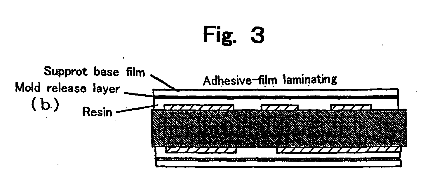
- Fig. 3 shows Steps (a) to (g) for a method of manufacturing a multilayered printed wiring board of the present invention including smoothing by stripping the support base film and subsequent formation of a plating layer and circuit, vertically in that order.
- thermosetting resin composition being solid at normal temperatures is not particularly limited as long as any resin composition comprises a thermosetting resin and/or a high polymer molecule as the main component, becomes softened by heating, has a film forming ability, and is thermally cured to satisfy the properties required of an interlayer insulating material, such as heat resistance and electric properties.
- an epoxy resin based material an acrylic resin based material, a polyimide resin based material, a polyamide-imide resin based material, a polycyanate resin based material, a polyester resin based material, a thermosetting polyphenylene ether resin based material, and the like.
- two or more of these materials can be combined for use.
- the adhesive film can be prepared by a known conventional method of applying a resin varnish dissolved in a predetermined organic solvent onto the mold release layer of a base film provided with a mold release layer as a support, and subsequently evaporating the solvent by heating and/or hot-air spraying, whereby a thermosetting resin composition being solid at normal temperatures is formed.
- support base film there may be exemplified polyethylene, polyvinyl chloride and other polyolefins; polyethylene terephthalate and other polyesters; polycarbonate; and further mold release paper, metal foils such as copper foil, and aluminum foil, and the like.
- the support base film is generally in thickness within a range of 10 to 100 ⁇ m.
- As the mold release layer a known conventional silicone based material, and a non-silicone based material can be used in accordance with the properties of resin varnish, and the thickness thereof is generally 3 ⁇ m or less.
- the thickness of the thermosetting resin composition being solid at normal temperatures is not less than the conductor thickness of the inner-layer circuit substrate to be laminated, and is generally within a range of the conductive thickness plus (10 to 120) ⁇ m.
- the adhesive film according to the present invention which film comprises a thermosetting resin composition being solid at normal temperatures and a support base film, is, when made, wound into a roll as it is, or after a mold release protective film has been further laminated on the other surface of the resin composition, and stored.
- a vacuum applicator manufactured by Nichigo Morton Kabushiki Kaisha a vacuum pressurizing laminator manufactured by Kabushiki Kaisha Meiki Seisakusho
- a vacuum rolling dry coater manufactured by Hitachi Techno-Engineering Kabushiki Kaisha a vacuum rolling dry coater manufactured by Hitachi Techno-Engineering Kabushiki Kaisha and other commercially available vacuum laminators can be used.
- the adhesive film is provided with a protective film, the adhesive film is, after the protective film has been removed, laminated on the pattern processed portion, on the resin composition layer side thereof by pressurizing and heating under a vacuum condition from the side of the support base film.
- laminating By performing laminating on condition that the thickness of the resin flow during laminating is not less than the conductor thickness of an inner-layer circuit, the inner-layer circuit pattern can be satisfactorily covered.
- laminating is preferably performed at a contact bonding temperature of 70 to 130°C, a contact bonding pressure of 1 to 11 kgf/cm 2 , and under reduced pressure of 10 millibars or less.
- the laminating can be performed either batch-wise or continuously with a roll.
- the resin composition is thermally cured with the support base film being attached thereto. Therefore, dirt or foreign matters fail to stick to the resin surface during being cured, whereby the conventional problem of foreign matter sticking is solved, and expensive facilities such as a clean oven and the like become unnecessary.
- perforating is performed with a laser and/or a drill.
- the thermal curing condition differs with resins, but is selected from a range of 100 to 200°C and 10 to 90 minutes. Step curing from a slightly low temperature to a high temperature is, above all, preferable in respect of finishing.
- the thermal curing is indispensable for uniformity of a hole shape in the subsequent perforating step, and for resistance to the organic solvent or the like contained in a conductive paste when such paste is used.
- perforating For perforating, commercially available carbonic acid gas, UV-YAG, excimer or other laser drill and/or a drill perforator is used, and the perforating is performed at the predetermined position(s) by a known conventional method. After perforating, the inside of the hole may be cleaned by mechanical treatments such as jet scrubbing, or chemical treatments such as soft etching.
- the support base film is provided with a mold release layer, the film can easily be stripped after the thermosetting resin composition has been thermally cured.
- the aforementioned steps are followed by the conventional process disclosed in Japanese Patent Application Laid-Open ( Kokai ) No. 87927/1999, or the same steps as those shown in Fig. 2, whereby a multilayered printed wiring board is completed.
- the above-described steps are followed by filling the hole(s) with the conductive paste.
- the conductive paste not only a commercially available metal powder paste such as a silver paste, a copper paste, or the like, but also a paste containing conductive particles, or the like, can be used.
- screen printing is generally carried out, but that is not limited thereto.
- the support base film perforated simultaneously with the resin composition layer serves as a high-precision contact mask, there can be obtained the excellent characteristic that no conductive paste sticks to the surface of the resin composition other than the hole portion. This enables selective electric connection by a conductive paste which has been heretofore difficult. Moreover, to enhance such filling into a small-diameter via, it is also preferable to perform a pressure reducing treatment step after printing.
- the step of stripping the support base film before thermally curing the conductive paste or the step of thermally curing the conductive paste before stripping the support base film, both in order to uncover the resin composition layer.
- the adhesive film of the present invention since the support base film is provided with the mold release layer, the film can be easily stripped after the thermosetting resin composition and/or the conductive paste has been thermally cured.
- the thermal curing conditions differ with the resins and conductive pastes, and are selected from a range of 100 to 200°C and 10 to 90 minutes.
- a step of polish-removing the sticking-out portion in the vicinity of the hole surface, of the hole filling ink or the conductive paste, during filling the hole(s) therewith, is essential.
- polishing step can be omitted.
- the support base film is stripped, the mold release layer is simultaneously stripped, but a part of the mold release layer remains on the resin composition surface in some cases. Even in this case, the sticking mold release layer can be removed in the next roughing step.
- the resin composition surface is subjected to a roughening treatment, and then a conductor layer is formed on the top layer by plating.
- a roughening treatment there may be mentioned a chemical treatment with permanganate, bichromate, ozone, hydrogen peroxide/sulfuric acid, nitric acid or other oxidizer, as well as buffing, sand blasting and other mechanical polishing, plasma etching, or the like.
- electroless plating, electrolytic plating or other plating is performed to form a conductor layer.
- a circuit can be formed without placing any restriction on the via or the through hole.
- a conductor circuit may be formed only by electroless plating.
- the varnish was applied onto a polyethylene terephthalate film with a thickness of 25 ⁇ m and provided with a silicone mold release layer ("Cerapeel BK" manufactured by Toyo Metallizing Kabushiki Kaisha) with a die coater in such amount that the resulting resin layer had, after dried, a thickness of 70 ⁇ m, and drying was performed at 80 to 120°C, whereby an adhesive film was obtained.
- a silicone mold release layer (“Cerapeel BK” manufactured by Toyo Metallizing Kabushiki Kaisha) with a die coater in such amount that the resulting resin layer had, after dried, a thickness of 70 ⁇ m, and drying was performed at 80 to 120°C, whereby an adhesive film was obtained.
- Example 1 From the results of the Example 1, it is understood that according to the method of the present invention, a clean insulating layer can be easily formed by using an adhesive film. Furthermore, from the results of the Examples 2 and 3, the hole filling screen print required heretofore for each pattern of the via and/or the through hole, and the surface polishing step can be omitted, and it is possible to easily manufacture multilayered printed wiring boards superior in surface smoothness by a buildup process.
- multilayered printed wiring boards can easily be manufactured in good yield and by the buildup process, with the use of an adhesive film.
Landscapes
- Engineering & Computer Science (AREA)
- Manufacturing & Machinery (AREA)
- Microelectronics & Electronic Packaging (AREA)
- Production Of Multi-Layered Print Wiring Board (AREA)
Abstract
Description
said method further comprising essentially the steps of:
said method further comprising essentially the steps of:
said method further comprising essentially the steps of:
Claims (3)
- A method of manufacturing a multilayered printed wiring board using an adhesive film comprising a support base film provided with a mold release layer and a thermosetting resin composition laminated on the surface of the mold release layer, said resin composition being provided with the same or smaller area as or than that of the support base film, provided with thermal fluidity and being solid at normal temperatures,
said method comprising the steps of:1) directly covering at least the pattern processed portion on one surface or both surfaces of a pattern processed circuit substrate with the resin composition layer of said adhesive film, and performing laminating by heating and pressurizing under a vacuum condition;2) thermally curing the resin composition with the support base film being attached thereto;3) uncovering the resin composition layer by stripping at least the support base film followed by performing perforating with a laser and/or a drill, or performing perforating with a laser and/or a drill followed by stripping at least the support base film;4) subjecting the resin composition surface to a roughing treatment; and5) subsequently plating the roughed surface, whereby a conductor layer is formed. - A method of manufacturing a multilayered printed wiring board using an adhesive film comprising a support base film provided with a mold release layer and a thermosetting resin composition laminated on the surface of the mold release layer, said resin composition being provided with the same or smaller area as or than that of the support base film, provided with thermal fluidity and being solid at normal temperatures,
said method comprising the steps of:1) directly covering at least the pattern processed portion on one surface or both surfaces of a pattern processed circuit substrate with the resin composition layer of said adhesive film, and performing laminating by heating and pressurizing under a vacuum condition;2) thermally curing the resin composition followed by performing perforating with a laser and/or a drill;3) charging a conductive paste into the resulting holes;4) uncovering the resin composition layer by stripping at least the support base film followed by thermally curing the conductive paste, or thermally curing the conductive paste followed by stripping at least the support base film;5) subjecting the resin composition surface to a roughing treatment; and6) subsequently plating the roughed surface, whereby a conductor layer is formed. - A method of manufacturing a multilayered printed wiring board using an adhesive film comprising a support base film provided with a mold release layer and a thermosetting resin composition laminated on the surface of the mold release layer, said resin composition being provided with the same or smaller area as or than that of the support base film, provided with thermal fluidity and being solid at normal temperatures,
said method comprising the steps of:1) directly covering at least the pattern processed portion on one surface or both surfaces of a pattern processed circuit substrate with the resin composition layer of said adhesive film, and performing lamination by heating and pressurizing under a vacuum condition; and2) thermally curing the resin composition with the support base film being attached thereto, whereby an insulation layer is formed.
Applications Claiming Priority (4)
| Application Number | Priority Date | Filing Date | Title |
|---|---|---|---|
| JP30709199 | 1999-10-28 | ||
| JP30709199 | 1999-10-28 | ||
| JP2000205132 | 2000-07-06 | ||
| JP2000205132A JP4300687B2 (en) | 1999-10-28 | 2000-07-06 | Manufacturing method of multilayer printed wiring board using adhesive film |
Publications (2)
| Publication Number | Publication Date |
|---|---|
| EP1096842A2 true EP1096842A2 (en) | 2001-05-02 |
| EP1096842A3 EP1096842A3 (en) | 2003-06-18 |
Family
ID=26564972
Family Applications (1)
| Application Number | Title | Priority Date | Filing Date |
|---|---|---|---|
| EP00309489A Withdrawn EP1096842A3 (en) | 1999-10-28 | 2000-10-27 | Method of manufacturing multilayered printed wiring board using adhesive film |
Country Status (6)
| Country | Link |
|---|---|
| US (1) | US6739040B1 (en) |
| EP (1) | EP1096842A3 (en) |
| JP (1) | JP4300687B2 (en) |
| KR (1) | KR20010051189A (en) |
| CN (1) | CN1302179A (en) |
| TW (1) | TW507510B (en) |
Cited By (6)
| Publication number | Priority date | Publication date | Assignee | Title |
|---|---|---|---|---|
| EP1622435A1 (en) * | 2004-07-28 | 2006-02-01 | ATOTECH Deutschland GmbH | Method of manufacturing an electronic circuit assembly using direct write techniques |
| US8440916B2 (en) | 2007-06-28 | 2013-05-14 | Intel Corporation | Method of forming a substrate core structure using microvia laser drilling and conductive layer pre-patterning and substrate core structure formed according to the method |
| US8877565B2 (en) | 2007-06-28 | 2014-11-04 | Intel Corporation | Method of forming a multilayer substrate core structure using sequential microvia laser drilling and substrate core structure formed according to the method |
| CN110121240A (en) * | 2019-04-30 | 2019-08-13 | 胜宏科技(惠州)股份有限公司 | A kind of full glue compression method of aluminum substrate substituting filling holes with resin |
| WO2020094492A1 (en) * | 2018-11-06 | 2020-05-14 | Bundesdruckerei Gmbh | Method for producing a via in a carrier foil, which is printed on both sides, using a multi-stage drilling process |
| WO2020094493A1 (en) * | 2018-11-06 | 2020-05-14 | Bundesdruckerei Gmbh | Method for producing a via in a carrier foil, which is printed on both sides, using a filling pressure |
Families Citing this family (49)
| Publication number | Priority date | Publication date | Assignee | Title |
|---|---|---|---|---|
| EP1009206A3 (en) * | 1998-12-02 | 2003-01-15 | Ajinomoto Co., Inc. | Method of vacuum-laminating adhesive film |
| JP4666830B2 (en) * | 2001-07-27 | 2011-04-06 | 京セラ株式会社 | Multilayer wiring board and manufacturing method thereof |
| KR20030016515A (en) * | 2001-08-21 | 2003-03-03 | 주식회사 코스모텍 | method for producing build-up multi-layer printed circuit board using a via filling |
| JP4707289B2 (en) * | 2001-09-27 | 2011-06-22 | 京セラ株式会社 | Manufacturing method of multilayer wiring board |
| JP2003158358A (en) * | 2001-11-26 | 2003-05-30 | Hitachi Via Mechanics Ltd | Laser drilling method and apparatus |
| JP3927516B2 (en) * | 2002-05-15 | 2007-06-13 | 積水化学工業株式会社 | Resin sheet |
| WO2004054337A1 (en) * | 2002-12-09 | 2004-06-24 | Noda Screen Co., Ltd. | Method for manufacturing printed wiring board |
| JP3811680B2 (en) * | 2003-01-29 | 2006-08-23 | 富士通株式会社 | Wiring board manufacturing method |
| TW592030B (en) * | 2003-04-29 | 2004-06-11 | Quanta Comp Inc | Functional module and manufacturing method thereof |
| TWI321975B (en) * | 2003-06-27 | 2010-03-11 | Ajinomoto Kk | Resin composition and adhesive film for multi-layered printed wiring board |
| CN100428871C (en) * | 2003-12-19 | 2008-10-22 | 财团法人工业技术研究院 | Method for forming metal wire pattern by ink-jet method |
| JP3961537B2 (en) * | 2004-07-07 | 2007-08-22 | 日本電気株式会社 | Manufacturing method of semiconductor mounting wiring board and manufacturing method of semiconductor package |
| KR100632560B1 (en) * | 2004-08-05 | 2006-10-09 | 삼성전기주식회사 | Parallel printed circuit board manufacturing method |
| CN1764345A (en) * | 2004-10-20 | 2006-04-26 | 华为技术有限公司 | Printed circuit board and its processing method |
| JP2006278774A (en) | 2005-03-29 | 2006-10-12 | Hitachi Cable Ltd | Method for manufacturing double-sided wiring board, double-sided wiring board, and base board thereof |
| KR100790350B1 (en) * | 2006-04-04 | 2008-01-02 | 엘지전자 주식회사 | Manufacturing method of printed circuit board |
| US20070246158A1 (en) * | 2006-04-21 | 2007-10-25 | 3M Innovative Properties Company | Wiring board, production process thereof and connection method using same |
| US7316605B1 (en) * | 2006-07-03 | 2008-01-08 | San Fang Chemical Industry Co., Ltd. | Sheet for mounting polishing workpiece and method for making the same |
| US7789738B2 (en) * | 2006-07-03 | 2010-09-07 | San Fang Chemical Industry Co., Ltd. | Sheet for mounting polishing workpiece and method for making the same |
| JP4993068B2 (en) * | 2006-08-21 | 2012-08-08 | 富士電機株式会社 | Insulating film formation method |
| US20080064310A1 (en) * | 2006-09-08 | 2008-03-13 | Chung-Chih Feng | Polishing pad having hollow fibers and the method for making the same |
| TWI337058B (en) * | 2007-02-16 | 2011-02-01 | Unimicron Technology Corp | Circuit board process |
| KR20090123944A (en) * | 2007-03-29 | 2009-12-02 | 스미토모 베이클리트 컴퍼니 리미티드 | Manufacturing method of insulation sheet with base material, multilayer printed wiring board, semiconductor device, and multilayer printed wiring board |
| US20090252876A1 (en) * | 2007-05-07 | 2009-10-08 | San Fang Chemical Industry Co., Ltd. | Sheet for mounting polishing workpiece and method for making the same |
| KR101530868B1 (en) | 2007-09-11 | 2015-06-23 | 아지노모토 가부시키가이샤 | Process for producing multilayer printed wiring board |
| TWI535355B (en) * | 2007-09-14 | 2016-05-21 | Ajinomoto Kk | Manufacturing method of multilayer printed circuit board |
| KR101601645B1 (en) | 2007-11-22 | 2016-03-09 | 아지노모토 가부시키가이샤 | Process for producing multilayered printed wiring board |
| JP4922207B2 (en) * | 2008-02-29 | 2012-04-25 | 積水化学工業株式会社 | Manufacturing method of multilayer insulating film and multilayer printed wiring board |
| CN101765341B (en) * | 2008-12-26 | 2012-01-04 | 南亚电路板股份有限公司 | Structure and method of laser-assisted circuit forming on substrate |
| JP5310849B2 (en) * | 2009-06-24 | 2013-10-09 | 富士通株式会社 | Wiring board manufacturing method |
| TW201110839A (en) * | 2009-09-04 | 2011-03-16 | Advanced Semiconductor Eng | Substrate structure and method for manufacturing the same |
| CN102104007B (en) * | 2009-12-21 | 2013-04-17 | 北大方正集团有限公司 | Method and equipment for manufacturing special circuit board |
| JP2011258838A (en) * | 2010-06-10 | 2011-12-22 | Fujitsu Ltd | Laminated circuit board, method of manufacturing the same, adhesive sheet, and method of manufacturing the same |
| WO2012164612A1 (en) * | 2011-05-31 | 2012-12-06 | パナソニック株式会社 | Method for manufacturing joined body, and joined body |
| JP5669773B2 (en) * | 2012-02-24 | 2015-02-18 | 三菱電機株式会社 | Curved substrate and method of manufacturing curved substrate |
| JP6300321B2 (en) * | 2012-08-07 | 2018-03-28 | 株式会社Joled | Manufacturing method of joined body and joined body |
| CN104290387B (en) * | 2013-07-16 | 2016-02-24 | 昆山雅森电子材料科技有限公司 | Antenna plate Special colored carburetion ink diaphragm and preparation method thereof |
| TWI663895B (en) | 2014-06-03 | 2019-06-21 | 日商三菱瓦斯化學股份有限公司 | Resin laminate for printed circuit board for forming fine via hole, multilayer printed circuit board with fine via hole in resin insulating layer and manufacturing method thereof |
| JP2016072333A (en) * | 2014-09-29 | 2016-05-09 | 日本ゼオン株式会社 | Manufacturing method of laminate |
| JP2016072334A (en) | 2014-09-29 | 2016-05-09 | 日本ゼオン株式会社 | Method for manufacturing laminate |
| JP2016072419A (en) | 2014-09-30 | 2016-05-09 | 日本ゼオン株式会社 | Manufacturing method of laminate |
| KR102476862B1 (en) | 2014-10-16 | 2022-12-14 | 아지노모토 가부시키가이샤 | Support body, adhesive sheet, laminated structure, semiconductor device, and method for manufacturing printed wiring board |
| JP6783614B2 (en) | 2016-10-11 | 2020-11-11 | 株式会社ディスコ | Wiring board manufacturing method |
| JP6821261B2 (en) | 2017-04-21 | 2021-01-27 | 株式会社ディスコ | Processing method of work piece |
| JP2020077670A (en) | 2018-11-05 | 2020-05-21 | 株式会社ディスコ | Manufacturing method of wiring board |
| TWI803738B (en) | 2019-03-11 | 2023-06-01 | 美商羅門哈斯電子材料有限公司 | Methods of manufacturing printed wire boards |
| JP7088133B2 (en) * | 2019-07-12 | 2022-06-21 | 味の素株式会社 | Manufacturing method of printed wiring board and resin sheet with inorganic layer |
| US11950378B2 (en) * | 2021-08-13 | 2024-04-02 | Harbor Electronics, Inc. | Via bond attachment |
| US12342470B2 (en) * | 2022-08-08 | 2025-06-24 | Reophotonics, Ltd. | Methods to fill through-holes of a substrate with metal paste |
Family Cites Families (13)
| Publication number | Priority date | Publication date | Assignee | Title |
|---|---|---|---|---|
| US3956041A (en) | 1972-07-11 | 1976-05-11 | Kollmorgen Corporation | Transfer coating process for manufacture of printing circuits |
| US5153987A (en) | 1988-07-15 | 1992-10-13 | Hitachi Chemical Company, Ltd. | Process for producing printed wiring boards |
| CA2006809A1 (en) | 1988-12-28 | 1990-06-28 | Toru Shirose | Laminate film having a thermosetting resin layer and use thereof for forming electrically insulating layer over conducting surface |
| US5057372A (en) * | 1989-03-22 | 1991-10-15 | The Dow Chemical Company | Multilayer film and laminate for use in producing printed circuit boards |
| DE3914727A1 (en) | 1989-04-28 | 1990-10-31 | Schering Ag | MULTIPLE LAYER PCB FOR FINE CONDUCTORS AND METHOD FOR THEIR PRODUCTION |
| US5344893A (en) | 1991-07-23 | 1994-09-06 | Ibiden Co., Ltd. | Epoxy/amino powder resin adhesive for printed circuit board |
| JP2601128B2 (en) | 1992-05-06 | 1997-04-16 | 松下電器産業株式会社 | Method of manufacturing circuit forming substrate and circuit forming substrate |
| JPH1027960A (en) * | 1996-07-09 | 1998-01-27 | Mitsui Mining & Smelting Co Ltd | Manufacturing method of multilayer printed wiring board |
| JP4117690B2 (en) | 1996-12-26 | 2008-07-16 | 味の素株式会社 | Method for producing multilayer printed wiring board using adhesive film for multilayer printed wiring board |
| ID19337A (en) | 1996-12-26 | 1998-07-02 | Ajinomoto Kk | INTER-PLATIN ADHESIVE FILM FOR MANUFACTURING BOARDS OF MOLD PLATED CABLES AND MANY MOLD PLATE CABLES USING THIS FILM |
| JPH10284840A (en) * | 1997-04-04 | 1998-10-23 | Hitachi Chem Co Ltd | Manufacture of multilayered printed wiring board |
| JP3568371B2 (en) | 1997-08-28 | 2004-09-22 | 日本電子株式会社 | Method for measuring peroxidase |
| JPH11340625A (en) * | 1998-03-23 | 1999-12-10 | Ajinomoto Co Inc | Method for vacuum lamination of adhesive film |
-
2000
- 2000-07-06 JP JP2000205132A patent/JP4300687B2/en not_active Expired - Lifetime
- 2000-10-23 KR KR1020000062262A patent/KR20010051189A/en not_active Withdrawn
- 2000-10-23 TW TW089122262A patent/TW507510B/en not_active IP Right Cessation
- 2000-10-25 CN CN00133154A patent/CN1302179A/en active Pending
- 2000-10-26 US US09/696,179 patent/US6739040B1/en not_active Expired - Lifetime
- 2000-10-27 EP EP00309489A patent/EP1096842A3/en not_active Withdrawn
Cited By (9)
| Publication number | Priority date | Publication date | Assignee | Title |
|---|---|---|---|---|
| EP1622435A1 (en) * | 2004-07-28 | 2006-02-01 | ATOTECH Deutschland GmbH | Method of manufacturing an electronic circuit assembly using direct write techniques |
| WO2006010639A3 (en) * | 2004-07-28 | 2006-10-26 | Atotech Deutschland Gmbh | Method of manufacturing an electronic circuit device through a direct write technique |
| US8440916B2 (en) | 2007-06-28 | 2013-05-14 | Intel Corporation | Method of forming a substrate core structure using microvia laser drilling and conductive layer pre-patterning and substrate core structure formed according to the method |
| US8877565B2 (en) | 2007-06-28 | 2014-11-04 | Intel Corporation | Method of forming a multilayer substrate core structure using sequential microvia laser drilling and substrate core structure formed according to the method |
| US9648733B2 (en) | 2007-06-28 | 2017-05-09 | Intel Corporation | Method of forming a substrate core structure using microvia laser drilling and conductive layer pre-patterning and substrate core structure formed according to the method |
| US10306760B2 (en) | 2007-06-28 | 2019-05-28 | Intel Corporation | Method of forming a substrate core structure using microvia laser drilling and conductive layer pre-patterning and substrate core structure formed according to the method |
| WO2020094492A1 (en) * | 2018-11-06 | 2020-05-14 | Bundesdruckerei Gmbh | Method for producing a via in a carrier foil, which is printed on both sides, using a multi-stage drilling process |
| WO2020094493A1 (en) * | 2018-11-06 | 2020-05-14 | Bundesdruckerei Gmbh | Method for producing a via in a carrier foil, which is printed on both sides, using a filling pressure |
| CN110121240A (en) * | 2019-04-30 | 2019-08-13 | 胜宏科技(惠州)股份有限公司 | A kind of full glue compression method of aluminum substrate substituting filling holes with resin |
Also Published As
| Publication number | Publication date |
|---|---|
| CN1302179A (en) | 2001-07-04 |
| US6739040B1 (en) | 2004-05-25 |
| EP1096842A3 (en) | 2003-06-18 |
| TW507510B (en) | 2002-10-21 |
| JP2001196743A (en) | 2001-07-19 |
| JP4300687B2 (en) | 2009-07-22 |
| KR20010051189A (en) | 2001-06-25 |
Similar Documents
| Publication | Publication Date | Title |
|---|---|---|
| US6739040B1 (en) | Method of manufacturing multilayered printed wiring board using adhesive film | |
| US6518513B1 (en) | Single-sided circuit board and method for manufacturing the same | |
| US6451710B1 (en) | Method of manufacturing multi-layer printed wiring board | |
| US6204456B1 (en) | Filling open through holes in a multilayer board | |
| WO2001005204A1 (en) | Method of manufacturing printed-circuit board | |
| WO2002005605A1 (en) | Carrier-foiled copper foil circuit, printed circuit board manufacturing method using the circuit, and printed circuit board | |
| US7800917B2 (en) | Printed wiring board | |
| JP3142270B2 (en) | Manufacturing method of printed wiring board | |
| US6938336B2 (en) | Methods of manufacturing board having throughholes filled with resin and multi-layered printed wiring board using the board | |
| JP2002033581A (en) | Manufacturing method of copper clad laminate | |
| JPS63199497A (en) | Multilayer printed interconnection board | |
| JPH1051113A (en) | Manufacture of multilayer printed-wiring board | |
| JPH05243735A (en) | Manufacture of multilayer wiring board | |
| US4927742A (en) | Multilayer printed wiring boards | |
| EP0087551A2 (en) | Method for stripping peel-apart conductive structure | |
| EP1353541B1 (en) | Circuit board and production method therefor | |
| JP2006066738A (en) | Multi-layer printed wiring board, copper-clad laminate therefor, and method for manufacturing the same | |
| JPH0936550A (en) | Manufacture of multilayer printed-wiring board | |
| JP2001068856A (en) | Insulation resin sheet and its manufacture | |
| US6022670A (en) | Process for high resolution photoimageable dielectric | |
| JP2005158974A (en) | Method for manufacturing multi-layer printed wiring board and sheet material for manufacturing the same | |
| JPH098458A (en) | Printed wiring board and manufacturing method thereof | |
| JP2000345119A (en) | Adhesive film and production of multilayered printed circuit board by using the same | |
| JPH10335834A (en) | Multilayer wiring board | |
| JP2000049440A (en) | Manufacture of printed wiring multilayer board |
Legal Events
| Date | Code | Title | Description |
|---|---|---|---|
| PUAI | Public reference made under article 153(3) epc to a published international application that has entered the european phase |
Free format text: ORIGINAL CODE: 0009012 |
|
| AK | Designated contracting states |
Kind code of ref document: A2 Designated state(s): AT BE CH CY DE DK ES FI FR GB GR IE IT LI LU MC NL PT SE |
|
| AX | Request for extension of the european patent |
Free format text: AL;LT;LV;MK;RO;SI |
|
| PUAL | Search report despatched |
Free format text: ORIGINAL CODE: 0009013 |
|
| AK | Designated contracting states |
Designated state(s): AT BE CH CY DE DK ES FI FR GB GR IE IT LI LU MC NL PT SE |
|
| AX | Request for extension of the european patent |
Extension state: AL LT LV MK RO SI |
|
| 17P | Request for examination filed |
Effective date: 20030717 |
|
| STAA | Information on the status of an ep patent application or granted ep patent |
Free format text: STATUS: THE APPLICATION HAS BEEN WITHDRAWN |
|
| AKX | Designation fees paid |
Designated state(s): DE FR GB |
|
| 18W | Application withdrawn |
Effective date: 20040122 |