EP1091340B1 - Verfahren und Einrichtung zur Steuerung eines organischen Dünnschicht-Elektrolumineszenzanzeigegerät - Google Patents
Verfahren und Einrichtung zur Steuerung eines organischen Dünnschicht-Elektrolumineszenzanzeigegerät Download PDFInfo
- Publication number
- EP1091340B1 EP1091340B1 EP00121697A EP00121697A EP1091340B1 EP 1091340 B1 EP1091340 B1 EP 1091340B1 EP 00121697 A EP00121697 A EP 00121697A EP 00121697 A EP00121697 A EP 00121697A EP 1091340 B1 EP1091340 B1 EP 1091340B1
- Authority
- EP
- European Patent Office
- Prior art keywords
- signal voltage
- display period
- electrode
- display
- data
- Prior art date
- Legal status (The legal status is an assumption and is not a legal conclusion. Google has not performed a legal analysis and makes no representation as to the accuracy of the status listed.)
- Expired - Lifetime
Links
- 239000010409 thin film Substances 0.000 title claims description 33
- 238000000034 method Methods 0.000 title claims description 15
- 239000011159 matrix material Substances 0.000 claims description 7
- 230000004044 response Effects 0.000 claims description 5
- 239000003990 capacitor Substances 0.000 description 13
- 238000010586 diagram Methods 0.000 description 11
- 239000010410 layer Substances 0.000 description 10
- 230000000694 effects Effects 0.000 description 4
- 239000010408 film Substances 0.000 description 4
- 238000002513 implantation Methods 0.000 description 2
- 238000012986 modification Methods 0.000 description 2
- 230000004048 modification Effects 0.000 description 2
- 239000000758 substrate Substances 0.000 description 2
- CMSGUKVDXXTJDQ-UHFFFAOYSA-N 4-(2-naphthalen-1-ylethylamino)-4-oxobutanoic acid Chemical compound C1=CC=C2C(CCNC(=O)CCC(=O)O)=CC=CC2=C1 CMSGUKVDXXTJDQ-UHFFFAOYSA-N 0.000 description 1
- 229910001316 Ag alloy Inorganic materials 0.000 description 1
- 229910000838 Al alloy Inorganic materials 0.000 description 1
- 229910000733 Li alloy Inorganic materials 0.000 description 1
- 229910000861 Mg alloy Inorganic materials 0.000 description 1
- 238000005266 casting Methods 0.000 description 1
- 238000007796 conventional method Methods 0.000 description 1
- 230000001419 dependent effect Effects 0.000 description 1
- 238000011161 development Methods 0.000 description 1
- 230000018109 developmental process Effects 0.000 description 1
- 238000007599 discharging Methods 0.000 description 1
- 239000011521 glass Substances 0.000 description 1
- 230000005525 hole transport Effects 0.000 description 1
- 239000001989 lithium alloy Substances 0.000 description 1
- 239000002184 metal Substances 0.000 description 1
- 239000011347 resin Substances 0.000 description 1
- 229920005989 resin Polymers 0.000 description 1
- 230000004043 responsiveness Effects 0.000 description 1
- 239000002356 single layer Substances 0.000 description 1
- 238000004528 spin coating Methods 0.000 description 1
- 238000001771 vacuum deposition Methods 0.000 description 1
Images


Classifications
-
- G—PHYSICS
- G09—EDUCATION; CRYPTOGRAPHY; DISPLAY; ADVERTISING; SEALS
- G09G—ARRANGEMENTS OR CIRCUITS FOR CONTROL OF INDICATING DEVICES USING STATIC MEANS TO PRESENT VARIABLE INFORMATION
- G09G3/00—Control arrangements or circuits, of interest only in connection with visual indicators other than cathode-ray tubes
- G09G3/20—Control arrangements or circuits, of interest only in connection with visual indicators other than cathode-ray tubes for presentation of an assembly of a number of characters, e.g. a page, by composing the assembly by combination of individual elements arranged in a matrix no fixed position being assigned to or needed to be assigned to the individual characters or partial characters
- G09G3/22—Control arrangements or circuits, of interest only in connection with visual indicators other than cathode-ray tubes for presentation of an assembly of a number of characters, e.g. a page, by composing the assembly by combination of individual elements arranged in a matrix no fixed position being assigned to or needed to be assigned to the individual characters or partial characters using controlled light sources
- G09G3/30—Control arrangements or circuits, of interest only in connection with visual indicators other than cathode-ray tubes for presentation of an assembly of a number of characters, e.g. a page, by composing the assembly by combination of individual elements arranged in a matrix no fixed position being assigned to or needed to be assigned to the individual characters or partial characters using controlled light sources using electroluminescent panels
- G09G3/32—Control arrangements or circuits, of interest only in connection with visual indicators other than cathode-ray tubes for presentation of an assembly of a number of characters, e.g. a page, by composing the assembly by combination of individual elements arranged in a matrix no fixed position being assigned to or needed to be assigned to the individual characters or partial characters using controlled light sources using electroluminescent panels semiconductive, e.g. using light-emitting diodes [LED]
- G09G3/3208—Control arrangements or circuits, of interest only in connection with visual indicators other than cathode-ray tubes for presentation of an assembly of a number of characters, e.g. a page, by composing the assembly by combination of individual elements arranged in a matrix no fixed position being assigned to or needed to be assigned to the individual characters or partial characters using controlled light sources using electroluminescent panels semiconductive, e.g. using light-emitting diodes [LED] organic, e.g. using organic light-emitting diodes [OLED]
- G09G3/3216—Control arrangements or circuits, of interest only in connection with visual indicators other than cathode-ray tubes for presentation of an assembly of a number of characters, e.g. a page, by composing the assembly by combination of individual elements arranged in a matrix no fixed position being assigned to or needed to be assigned to the individual characters or partial characters using controlled light sources using electroluminescent panels semiconductive, e.g. using light-emitting diodes [LED] organic, e.g. using organic light-emitting diodes [OLED] using a passive matrix
-
- G—PHYSICS
- G09—EDUCATION; CRYPTOGRAPHY; DISPLAY; ADVERTISING; SEALS
- G09G—ARRANGEMENTS OR CIRCUITS FOR CONTROL OF INDICATING DEVICES USING STATIC MEANS TO PRESENT VARIABLE INFORMATION
- G09G2310/00—Command of the display device
- G09G2310/02—Addressing, scanning or driving the display screen or processing steps related thereto
- G09G2310/0243—Details of the generation of driving signals
- G09G2310/0251—Precharge or discharge of pixel before applying new pixel voltage
-
- G—PHYSICS
- G09—EDUCATION; CRYPTOGRAPHY; DISPLAY; ADVERTISING; SEALS
- G09G—ARRANGEMENTS OR CIRCUITS FOR CONTROL OF INDICATING DEVICES USING STATIC MEANS TO PRESENT VARIABLE INFORMATION
- G09G2330/00—Aspects of power supply; Aspects of display protection and defect management
- G09G2330/02—Details of power systems and of start or stop of display operation
- G09G2330/021—Power management, e.g. power saving
- G09G2330/023—Power management, e.g. power saving using energy recovery or conservation
-
- G—PHYSICS
- G09—EDUCATION; CRYPTOGRAPHY; DISPLAY; ADVERTISING; SEALS
- G09G—ARRANGEMENTS OR CIRCUITS FOR CONTROL OF INDICATING DEVICES USING STATIC MEANS TO PRESENT VARIABLE INFORMATION
- G09G2340/00—Aspects of display data processing
- G09G2340/16—Determination of a pixel data signal depending on the signal applied in the previous frame
Definitions
- the present invention relates to a driving device and a driving method of an organic thin film electroluminescent (EL) display.
- the present invention relates to a driving device and a driving method of an organic thin film EL display with reduced power consumption.
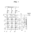
- Fig. 1 is a circuit diagram of the prior art showing an example of a conventional configuration where data electrodes Xi and scanning electrodes Yj arrayed in a matrix are passively driven. A blanking period is provided between display periods. All the switching circuits 9i, 7j are switched to the ground side in response to a blanking pulse transmitted during this period. As a result, residual electric charges accumulated in all the data lines are discharged.
- Fig. 1 is a circuit diagram of the prior art showing an example of a conventional configuration where data electrodes Xi and scanning electrodes Yj arrayed in a matrix are passively driven. A blanking period is provided between display periods. All the switching circuits 9i, 7j are switched to the ground side in response to a blanking pulse transmitted during this period. As a result, residual electric charges accumulated in all the data lines are discharged.
- Fig. 1 is a circuit diagram of the prior art showing an example of a conventional configuration where data electrodes Xi and scanning electrodes Yj arrayed in
- reference numeral 2 is an image memory
- reference numeral 8 is a driving circuit
- reference numeral 4 is an organic thin film EL display
- reference numeral 5 is a scanning circuit
- reference numeral 51 is a sift register
- reference numeral 6j is an OR circuit.
- a pixel P(i, j) is taken for example here. If a scanning electrode Yj to which this pixel P(i, j) belongs is selected, that is, the pixel P(i, j) is in a turned-off state during a display period Tj, a reverse bias is applied to the parallel capacitors of all the pixels P(i, 1) to P(i, j-1) and P(i, j+1) to P(i, n) belonging to a data electrode Xi except for the pixel P(i, j).
- a certain effect can be made by providing a blanking period tj between the display period Tj and the display period T(j+1) and applying the data electrode Xi to the ground potential during this blanking period to cancel the charge of the reverse-biased parallel capacitor of the pixel P(i, 1) to P(i, j-1) and P(i, j+1) to P(i, n).
- An object of the present invention is to provide a driving device and a driving method of an organic thin film EL display with power consumption reduced by a configuration where electric charges accumulated in a display element are used to assist a display element to emit light during the next display period.
- Patent Abstracts of Japan, Vol. 014, No. 317 (P-1073 ) & JP 02 103590 A discloses a driving method for a matrix type display.
- a data comparator circuit is added to the data driver circuit which compares the data at the time of present scanning and the data at the time of next scanning to determine whether the charge of the EL cell is discharged or held.
- an image signal voltage S(i, j) for the current display period is larger than an image signal voltage S(i, j+1) for the next display period
- the controller controls the data electrode on the currently displaying scanning electrode so that residual electric charges are discharged during the blanking period immediately before the next display period. If an image signal voltage S(i, j) for the current display period is equal to or less than an image signal voltage S(i, j+1) for the next display period, the controller controls the data electrode so that the residual electric charges are not discharged.
- controller also controls a discharge circuit which holds the data electrode at the ground level, for example.
- an image memory having a memory capacity at least enough for 2 x m (m: the number of data electrodes).
- the signal voltage applied to each data electrode on the currently displaying scanning electrode for a display period and the signal voltage applied to the data electrode on the scanning electrode for the next display period are stored in this image memory so that the comparator can compare the data in the image memory.
- the driving device of an organic film EL display also has the same number of discharge circuits as, for example, the number of data electrodes (m).
- the driving device and the driving method of an organic thin film EL display of the present invention According to the driving device and the driving method of an organic thin film EL display of the present invention, residual electric charges which are conventionally discharged uniformly from all the data electrodes during the blanking period are discharged individually from each data electrode. That is, since residual electric charges do not need to be discharged from a data electrode during the blanking period if the signal voltage for the current display period is not larger than the signal voltage for the next display period, a wasted outflow of electric charges can be prevented by detecting such an electrode.
- the first effect of the present invention is electric power saving. It is particularly effective to a display pattern such that all of display elements (pixels) are turned on or the like, where signal voltage applied to each data electrode does not decrease.
- the second effect of the present invention is the improvement of responsiveness when a pixel emits light and the improvement of brightness since residual electric charges which are not discharged during the blanking period are contributed to the charge of the parallel capacitor of a pixel which should emit light during the next display period.
- the driving device of an organic thin film EL display according to the present invention is characterized in that, when data electrodes and scanning electrodes arrayed in a matrix are passively driven, residual electric charges which are uniformly discharged from all the data electrodes in a conventional manner during a blanking period are discharged individually from each data electrode.
- the discharge circuit 3i controls the quantity of residual electric charges discharged from the data electrode Xi depending on this comparison result. That is, the data electrode Xi is controlled depending on the comparison result so that residual electric charges are discharged or not.
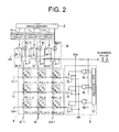
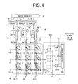
- Figs. 2 to 6 show the driving device of organic thin film EL display according to the example which is not part of the present invention.
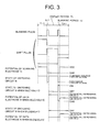
- Fig. 3 is a timing chart of the example which is not part illustrating an operation of the example which is not part of the present invention.
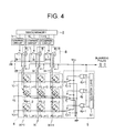
- Fig. 4 is a circuit diagram illustrating a current flow and a state that electric charges are accumulated during a display period Tj in the example which is not part of the present invention.
- Fig. 5 is a circuit diagram illustrating a state that electric charges are discharged during a blanking period tj when S(i, j) > S(i, j+1).
- Fig. 6 is a circuit diagram illustrating a current flow and a state that electric charges are transferred during a display period T(j+1) when S(i, j) ⁇ S(i, j+1).
- the driving device has comparator 1i for comparing the signal voltage S(i, j) applied to a display element P(i, j) on a predetermined data electrode Xi on a scanning electrode Yj for the current display period and the signal voltage S(i, j+1) applied to the display element P(i, j+1) on this data electrode Xi and on the scanning electrode Y(j+1) for the next display period.
- the driving apparatus also has controller 3i for controlling a quantity of residual electric charges discharged from the data electrode on the currently displaying scanning electrode Yj during a blanking period immediately before the next display period depending on the comparison result by the comparator.
- the controller 3i controls the data electrode Xi on the currently displaying scanning electrode Yj so that residual electric charges are discharged during the blanking period immediately before the next display period.
- the controller 3i controls the data electrode Xi so that the residual electric charges are not discharged.
- the controller 3i controls a discharge circuit which holds the data electrode in the ground level.
- An image memory 2 having a memory capacity at least enough for 2 x m (m: the number of data electrodes) is also provided.
- the signal voltage S(1, j) to S(m, j) applied to each data electrode X1 to Xm on scanning electrode Yj for the current display period and the signal voltage S(1, j+1) to S(m, j+1) applied to each data electrode X1 to Xm on the scanning electrode Y(j+1) for the next display period are stored in this image memory 2 so that the comparator 11 to 1m can compare the data in the image memory 2.
- the driving apparatus for driving an organic thin film EL display is also characterized by having the same number of discharge circuits as the number of data electrodes (m).
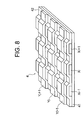
- Fig. 8 is a perspective view showing a structure of an organic thin film EL display.
- FIG. 8 shows a common structure of an organic thin film EL display 4 driven by the present invention.
- a substrate 41 light-transmittable glass, resin or the like is used.
- As a data electrode Xi light-transmittable ITO, NESA film, metal thin film or the like is used.
- As a scanning electrode Yj Ag/Mg alloy, Al/Li alloy or the like is used.
- the organic thin film layer 42 is constituted by a plurality of organic laminated layer film composed of a hole implantation layer, hole transport layer, light-emitting layer, electron transport layer, electron implantation layer and so forth or a single layer film composed of only a light-emitting layer and is formed by a thin film forming technique such as a vacuum deposition method, spin-coating method, casting method or the like.
- a thin film forming technique such as a vacuum deposition method, spin-coating method, casting method or the like.
- a pixel P (i, j) is represented by a diode symbol and a capacitor connected in parallel with the diode.
- An image memory 2 is a memory circuit having a memory capacity at least enough for 2 x m (m: the number of pixels) and can be achieved by a field memory, FIFO, DRAM, SRAM or the like.
- a scan circuit 5 is composed of a shift register 51, an OR circuit 6j and a switching circuit 7j.
- a driving circuit 8 is constituted by a current source circuit 8i for supplying current to the data electrode Xi depending on the image signal voltage S(i, j) and a switching circuit 9i.
- a compare circuit 1i compares the image signal voltage S(i, j) for the current display period and the image signal voltage S(i, j+1) for the next display period read from the image memory 2 and controls the discharge circuit 3i during a blanking period.
- the simplest form of a discharge circuit 3i is a switching circuit.
- Fig. 3 is a timing chart showing an operation of each part of Fig. 2 .
- a switching circuit 7j is controlled by a shift pulse and a blanking pulse so that the scanning electrode Yj is connected to the ground side when the control input is at a high level and connected to the power supply voltage VCC side when the control input is at a low level.
- the switching circuit 9i is controlled only by a blanking pulse so that the data electrode Xi is connected to the discharge circuit 3i when the control input is at a high level and connected to the current source circuit 8i when the control input is at a low level.
- all the scanning electrodes Yj have a ground potential by a blanking pulse applied to the OR circuit 6j.
- the data electrode Xi is connected to the discharge circuit 3i side, but the discharge circuit 3i is controlled by the compare circuit 1i as follows depending on the comparison result of the displayed image signal voltage S(i, j) and the image signal voltage S(i, j+1) for the next scanning period.
- the discharge circuit 3i composed of switching circuits is turned on and electric charges accumulated in the pixel P (i, j) are discharged.
- the discharge path is constituted in the order of the parallel capacitor of the pixel P (i, j), the switching circuit 9i, the discharge circuit 3i, the ground, the switching circuit 7j and the parallel capacitor of the pixel P (i, j).
- the discharge circuit 3i is turned off, electric charges accumulated in the pixel P(i, j) are not discharged and the parallel capacitor of the pixel P(i, j+1) is charged during the next display period T(j+1).
- the charge path is constituted in the order of the power supply (VCC), the switching circuit 7j, the parallel capacitor of the pixel P(i, j), the parallel capacitor of the pixel P(i, j+1), the switching circuit 7(j+1) and the ground.
- Fig. 7 is a circuit diagram showing a driving device and a driving method of an organic thin film EL display according to an embodiment of the present invention.
- Fig. 7 shows a driving device of an organic thin film EL display constituted such that display elements P(i, j) composed of organic thin film EL light-emitting elements are connected to respective intersections of data electrodes Xi and scanning electrodes Yj arrayed in a matrix. While a scanning electrode is scanned at predetermined periods, the display element emits light in response to a signal applied to the data electrode in synchronization with the scanning.
- the driving device also has a controller (discharge circuit 30i) for controlling a quantity of residual electric charges discharged from the data electrode on the currently displaying scanning electrode to a predetermined value during a blanking period immediately before the next display period depending on the comparison result by the comparator.
- a controller discharge circuit 30i for controlling a quantity of residual electric charges discharged from the data electrode on the currently displaying scanning electrode to a predetermined value during a blanking period immediately before the next display period depending on the comparison result by the comparator.
- the discharge circuit 30i has a resistance and the comparator circuit 1i controls the resistance value of the discharge circuit 30i.
- the discharge circuit 30i is a current control circuit.
Landscapes
- Engineering & Computer Science (AREA)
- Physics & Mathematics (AREA)
- Computer Hardware Design (AREA)
- General Physics & Mathematics (AREA)
- Theoretical Computer Science (AREA)
- Control Of Indicators Other Than Cathode Ray Tubes (AREA)
- Control Of El Displays (AREA)
- Electroluminescent Light Sources (AREA)
Claims (5)
- Ansteuervorrichtung für ein organisches Dünnschicht-Elektrolumineszenz (EL)-Anzeigegerät mit Anzeigeelementen, die aus organischen, Licht emittierenden Dünnschicht-EL-Elementen (P) zusammengesetzt sind,
die mit den jeweiligen Schnittpunkten von Datenelektroden (X) und Abtastelektroden (Y) verbunden sind, welche in einer Matrix angeordnet sind; wobei während des Abtastens der Abtastelektrode in vorbestimmten Perioden die Anzeigeelemente Licht in Antwort auf ein Signal emittieren, das an die Datenelektrode (X) synchron mit diesem Abtasten angelegt wird; wobei die Ansteuervorrichtung aufweist
einen Komparator (1), der so ausgebildet ist, dass er eine an das Anzeigeelement an eine vorbestimmte Datenelektrode (X) und an die Abtastelektrode für die laufende Anzeigeperiode angelegte Signalspannung und eine Signalspannung, die an das Anzeigeelement an dieser Datenelektrode und an die Abtastelektrode für die nächste Anzeigeelektrode angelegt wird, vergleicht; und
eine Steuerung (30), die so ausgebildet ist, dass sie die Menge der elektrischen Restladungen, die von der Datenelektrode an der derzeitigen Anzeigeabtastelektrode während einer Dunkelsteuerungsperiode unmittelbar vor der nächsten Anzeigeperiode ausgegeben wird, in Abhängigkeit von dem Vergleichsergebnis durch den Komparator (1) steuert,
dadurch gekennzeichnet, dass,
wenn der Komparator (1) detektiert, dass die Signalspannung für die derzeitige Anzeigeperiode kleiner als oder gleich der Signalspannung für die nächste Anzeigeperiode ist, die Steuerung (30) eine Steuerung so durchführt, dass keine elektrischen Restladungen ausgegeben werden, und wenn der Komparator (1) detektiert, dass die Signalspannung für die derzeitige Anzeigeperiode größer als die Signalspannung für die nächste Anzeigeperiode ist, die Steuerung (30) die Menge der Entladung der elektrischen Restladungen in Übereinstimmung mit der Differenz zwischen der Signalspannung für die derzeitige Anzeigeperiode und der Signalspannung für die nächste Anzeigeperiode steuert. - Ansteuervorrichtung eines organischen Dünnschicht-EL-Anzeigegerätes nach Anspruch 1,
dadurch gekennzeichnet, dass
die Steuerung (3, 30) eine Entladeschaltung steuert, die die Datenelektrode auf dem Massepegel hält. - Ansteuervorrichtung eines organischen Dünnschicht-EL-Anzeigegerätes nach Anspruch 1 oder 2, weiterhin gekennzeichnet durch
einen Bildspeicher (2) mit einer Speicherkapazität, die wenigstens ausreichend für 2 x m ist, wobei m die Zahl der Datenelektroden ist;
wobei die Signalspannung, welche an jede der Datenelektroden (X) an der derzeitigen Anzeigeabtastelektrode für eine Anzeigeperiode angelegt wird, in dem Bildspeicher (2) gespeichert wird;
die Signalspannung, welche an jede der Datenelektroden an der Abtastelektrode für die nächste Anzeigeperiode angelegt wird, gespeichert wird, und
der Komparator (1) die Daten in dem Bildspeicher vergleicht. - Ansteuervorrichtung für ein organisches Dünnschicht-EL-Anzeigegerät nach Anspruch 3, dadurch gekennzeichnet, dass
die Anzahl dieser Entladeschaltungen die gleiche wie die Anzahl der Datenelektroden (m) ist. - Verfahren zum Ansteuern eines organischen Dünnschicht-EL-Anzeigegerätes, das Anzeigeelemente aufweist, die aus organischen, Licht emittierenden Dünnschicht-EL-Elementen bestehen, die mit den jeweiligen Schnittpunkten der Datenelektroden (X) und der Abtastelektroden (Y) verbunden sind, welche in einer Matrix angeordnet sind;
wobei eine Abtastelektrode in vorbestimmten Perioden abgetastet wird, während ein Anzeigeelement Licht in Antwort auf ein Signal emittiert, das an die Datenelektrode synchron mit diesem Abtasten angelegt wird; wobei das Verfahren die Schritte aufweist:Vergleichen einer Signalspannung, die an das Anzeigeelement an einer vorbestimmten Datenelektrode und an der Abtastelektrode für die derzeitige Anzeigeperiode angelegt ist, und einer Signalspannung, die an das Anzeigeelement an der Datenelektrode und an der Abtastelektrode für die nächste Anzeigeperiode angelegt wird; undSteuern der Menge der elektrischen Restladungen, die von der Datenelektrode an der derzeitigen Anzeigeabtastelektrode während einer Dunkelsteuerungsperiode unmittelbar vor der nächsten Anzeigeperiode ausgegeben werden, in Abhängigkeit von dem Vergleichsergebnis durch den Vergleichsschritt,dadurch gekennzeichnet, dass,
wenn der Vergleichsschritt anzeigt, dass die Signalspannung für die derzeitige Anzeigeperiode kleiner als oder gleich der Signalspannung für die nächste Anzeigeperiode ist, die Steuerung so durchgeführt wird, dass keine elektrischen Restladungen ausgegeben werden, und wenn der Vergleichsschritt anzeigt, dass die Signalspannung für die derzeitige Anzeigeperiode größer als die Signalspannung für die nächste Anzeigeperiode ist, der Steuerungsschritt die Menge der ausgegebenen elektrischen Restladungen in Übereinstimmung mit der Differenz zwischen der Signalspannung für die derzeitige Anzeigeperiode und der Signalspannung für die nächste Anzeigeperiode steuert.
Applications Claiming Priority (2)
| Application Number | Priority Date | Filing Date | Title |
|---|---|---|---|
| JP28416799 | 1999-10-05 | ||
| JP28416799A JP3341735B2 (ja) | 1999-10-05 | 1999-10-05 | 有機薄膜el表示装置の駆動装置とその駆動方法 |
Publications (3)
| Publication Number | Publication Date |
|---|---|
| EP1091340A2 EP1091340A2 (de) | 2001-04-11 |
| EP1091340A3 EP1091340A3 (de) | 2002-12-04 |
| EP1091340B1 true EP1091340B1 (de) | 2008-03-19 |
Family
ID=17675061
Family Applications (1)
| Application Number | Title | Priority Date | Filing Date |
|---|---|---|---|
| EP00121697A Expired - Lifetime EP1091340B1 (de) | 1999-10-05 | 2000-10-04 | Verfahren und Einrichtung zur Steuerung eines organischen Dünnschicht-Elektrolumineszenzanzeigegerät |
Country Status (5)
| Country | Link |
|---|---|
| US (1) | US6369516B1 (de) |
| EP (1) | EP1091340B1 (de) |
| JP (1) | JP3341735B2 (de) |
| KR (1) | KR100380826B1 (de) |
| DE (1) | DE60038348T2 (de) |
Families Citing this family (43)
| Publication number | Priority date | Publication date | Assignee | Title |
|---|---|---|---|---|
| JP3737889B2 (ja) * | 1998-08-21 | 2006-01-25 | パイオニア株式会社 | 発光ディスプレイ装置および駆動方法 |
| MY124036A (en) | 1999-07-08 | 2006-06-30 | Nichia Corp | Image display apparatus and its method of operation |
| FI110946B (fi) * | 2000-05-25 | 2003-04-30 | Raisio Chem Oy | Uudentyyppinen kationinen tärkkelystuote, tuotteen valmistaminen ja käyttö |
| JP3867835B2 (ja) * | 2000-06-05 | 2007-01-17 | パイオニア株式会社 | 表示装置 |
| JP3485175B2 (ja) * | 2000-08-10 | 2004-01-13 | 日本電気株式会社 | エレクトロルミネセンスディスプレイ |
| US6608448B2 (en) * | 2001-01-31 | 2003-08-19 | Planar Systems, Inc. | Organic light emitting device |
| US6943761B2 (en) * | 2001-05-09 | 2005-09-13 | Clare Micronix Integrated Systems, Inc. | System for providing pulse amplitude modulation for OLED display drivers |
| US6777885B2 (en) * | 2001-10-12 | 2004-08-17 | Semiconductor Energy Laboratory Co., Ltd. | Drive circuit, display device using the drive circuit and electronic apparatus using the display device |
| US7180479B2 (en) * | 2001-10-30 | 2007-02-20 | Semiconductor Energy Laboratory Co., Ltd. | Signal line drive circuit and light emitting device and driving method therefor |
| US7742064B2 (en) | 2001-10-30 | 2010-06-22 | Semiconductor Energy Laboratory Co., Ltd | Signal line driver circuit, light emitting device and driving method thereof |
| US7576734B2 (en) * | 2001-10-30 | 2009-08-18 | Semiconductor Energy Laboratory Co., Ltd. | Signal line driving circuit, light emitting device, and method for driving the same |
| US7193619B2 (en) * | 2001-10-31 | 2007-03-20 | Semiconductor Energy Laboratory Co., Ltd. | Signal line driving circuit and light emitting device |
| EP1506696A1 (de) * | 2002-05-16 | 2005-02-16 | Koninklijke Philips Electronics N.V. | Led kapazitanzentladung mit begrenztem strom |
| JP3498745B1 (ja) * | 2002-05-17 | 2004-02-16 | 日亜化学工業株式会社 | 発光装置及びその駆動方法 |
| JP2004138978A (ja) * | 2002-10-21 | 2004-05-13 | Pioneer Electronic Corp | 表示パネル駆動装置 |
| FR2846454A1 (fr) * | 2002-10-28 | 2004-04-30 | Thomson Licensing Sa | Dispositif de visualisation d'images a recuperation d'energie capacitive |
| JP4170293B2 (ja) * | 2003-01-17 | 2008-10-22 | 株式会社半導体エネルギー研究所 | 半導体装置 |
| KR100884790B1 (ko) | 2003-04-11 | 2009-02-23 | 삼성모바일디스플레이주식회사 | 개선된 페이드-아웃 및 페이드-인 동작을 위한 전계발광디스플레이 패널의 구동 방법 |
| KR100903099B1 (ko) * | 2003-04-15 | 2009-06-16 | 삼성모바일디스플레이주식회사 | 효율적으로 부팅이 수행되는 전계발광 디스플레이 패널의구동 방법 및 장치 |
| US7961160B2 (en) * | 2003-07-31 | 2011-06-14 | Semiconductor Energy Laboratory Co., Ltd. | Display device, a driving method of a display device, and a semiconductor integrated circuit incorporated in a display device |
| KR100565664B1 (ko) * | 2004-01-10 | 2006-03-29 | 엘지전자 주식회사 | 평판 디스플레이 패널 구동 장치 및 방법 |
| JP2005258128A (ja) * | 2004-03-12 | 2005-09-22 | Tohoku Pioneer Corp | 自発光表示モジュールおよび同モジュールを搭載した電子機器、ならびに同モジュールにおける欠陥状態の検証方法 |
| KR100611882B1 (ko) * | 2004-06-25 | 2006-08-11 | 삼성에스디아이 주식회사 | 영상 표시장치 및 방법 |
| JP2006251457A (ja) * | 2005-03-11 | 2006-09-21 | Tohoku Pioneer Corp | 自発光パネルの駆動装置および駆動方法 |
| KR101157252B1 (ko) * | 2005-06-20 | 2012-06-15 | 엘지디스플레이 주식회사 | 액정표시장치 및 그 구동방법 |
| US7791567B2 (en) * | 2005-09-15 | 2010-09-07 | Lg Display Co., Ltd. | Organic electroluminescent device and driving method thereof |
| KR100656842B1 (ko) | 2005-11-17 | 2006-12-14 | 엘지전자 주식회사 | 유기 전계 발광 소자 및 이를 구동하는 방법 |
| US20070120777A1 (en) | 2005-11-30 | 2007-05-31 | Lg Electronics Inc. | Light emitting device and method of driving the same |
| TWI348675B (en) * | 2006-04-07 | 2011-09-11 | Himax Tech Ltd | Method for driving display |
| US7898508B2 (en) | 2006-04-28 | 2011-03-01 | Lg Display Co., Ltd. | Light emitting device and method of driving the same |
| KR100756275B1 (ko) | 2006-04-28 | 2007-09-06 | 엘지전자 주식회사 | 발광 소자 및 이를 구동하는 방법 |
| KR100736574B1 (ko) * | 2006-04-28 | 2007-07-06 | 엘지전자 주식회사 | 발광 소자 및 이를 구동하는 방법 |
| JP4936340B2 (ja) * | 2006-10-25 | 2012-05-23 | パイオニア株式会社 | 表示装置および表示装置の駆動方法 |
| US8223137B2 (en) * | 2006-12-14 | 2012-07-17 | Lg Display Co., Ltd. | Liquid crystal display device and method for driving the same |
| TW200830258A (en) * | 2007-01-12 | 2008-07-16 | Richtek Techohnology Corp | Driving apparatus for organic light-emitting diode panel |
| JP4990315B2 (ja) * | 2008-03-20 | 2012-08-01 | アナパス・インコーポレーテッド | ブランク期間にクロック信号を伝送するディスプレイ装置及び方法 |
| US20090251391A1 (en) * | 2008-04-02 | 2009-10-08 | Solomon Systech Limited | Method and apparatus for power recycling in a display system |
| WO2012048407A1 (en) * | 2010-10-11 | 2012-04-19 | Scobil Industries Corp. | Integrated drive circuit for multi-segment electroluminescent displays |
| JP6032118B2 (ja) * | 2013-04-26 | 2016-11-24 | 日亜化学工業株式会社 | 表示装置 |
| US9343007B2 (en) * | 2013-05-21 | 2016-05-17 | My-Semi Inc. | Switch structure and method of charging and discharing scan lines of an LED display |
| JP6011942B2 (ja) * | 2013-12-17 | 2016-10-25 | 双葉電子工業株式会社 | 走査線駆動装置、表示装置、走査線駆動方法 |
| CN113571006A (zh) | 2020-04-29 | 2021-10-29 | 联咏科技股份有限公司 | 一种显示装置及其驱动器 |
| GB2607627B (en) * | 2021-06-10 | 2024-01-24 | Advanced Risc Mach Ltd | Circuitry and method |
Family Cites Families (6)
| Publication number | Priority date | Publication date | Assignee | Title |
|---|---|---|---|---|
| JPH02103590A (ja) * | 1988-10-13 | 1990-04-16 | Nec Kansai Ltd | マトリクス型ディスプレイの駆動方法 |
| JPH0748143B2 (ja) * | 1988-12-28 | 1995-05-24 | シャープ株式会社 | 表示装置の駆動方法 |
| US5552677A (en) * | 1995-05-01 | 1996-09-03 | Motorola | Method and control circuit precharging a plurality of columns prior to enabling a row of a display |
| JP3507239B2 (ja) * | 1996-02-26 | 2004-03-15 | パイオニア株式会社 | 発光素子の駆動方法及び装置 |
| US5923308A (en) * | 1996-11-12 | 1999-07-13 | Motorola, Inc. | Array of leds with active pull down shadow canceling circuitry |
| JP4081912B2 (ja) * | 1999-03-31 | 2008-04-30 | 株式会社デンソー | ディスプレイ装置 |
-
1999
- 1999-10-05 JP JP28416799A patent/JP3341735B2/ja not_active Expired - Fee Related
-
2000
- 2000-09-29 US US09/676,846 patent/US6369516B1/en not_active Expired - Lifetime
- 2000-10-04 DE DE60038348T patent/DE60038348T2/de not_active Expired - Lifetime
- 2000-10-04 KR KR10-2000-0058069A patent/KR100380826B1/ko not_active Expired - Lifetime
- 2000-10-04 EP EP00121697A patent/EP1091340B1/de not_active Expired - Lifetime
Also Published As
| Publication number | Publication date |
|---|---|
| US6369516B1 (en) | 2002-04-09 |
| DE60038348T2 (de) | 2009-03-12 |
| JP3341735B2 (ja) | 2002-11-05 |
| KR100380826B1 (ko) | 2003-04-18 |
| DE60038348D1 (de) | 2008-04-30 |
| JP2001109428A (ja) | 2001-04-20 |
| KR20010050818A (ko) | 2001-06-25 |
| EP1091340A3 (de) | 2002-12-04 |
| EP1091340A2 (de) | 2001-04-11 |
Similar Documents
| Publication | Publication Date | Title |
|---|---|---|
| EP1091340B1 (de) | Verfahren und Einrichtung zur Steuerung eines organischen Dünnschicht-Elektrolumineszenzanzeigegerät | |
| US7187375B2 (en) | Apparatus and method of generating gamma voltage | |
| US6351076B1 (en) | Luminescent display panel drive unit and drive method thereof | |
| US20030001804A1 (en) | Drive method and drive apparatus for a display panel | |
| EP1094438A1 (de) | Anzeigegerät mit aktiver latrix und Steuerschaltung dafür | |
| US20090251391A1 (en) | Method and apparatus for power recycling in a display system | |
| JP2004046088A (ja) | 発光装置及びその駆動方法 | |
| US6369515B1 (en) | Display apparatus with capacitive light-emitting devices and method of driving the same | |
| US7183719B2 (en) | Method for driving organic light emitting display panel | |
| US7999771B2 (en) | Organic light emitting display and driving method thereof | |
| US7133006B2 (en) | Display panel drive apparatus | |
| US20030184503A1 (en) | Method for aging display apparatus and electronic equipment using the method | |
| EP1876581B1 (de) | Flachbildschirm und Ansteuerverfahren dafür | |
| JP2003195806A (ja) | 有機エレクトロルミネッセンス素子の発光回路及び表示装置 | |
| US20060007070A1 (en) | Driving circuit and driving method for electroluminescent display | |
| US6229267B1 (en) | Display apparatus with capacitive light-emitting devices and method of driving the same | |
| US20070252791A1 (en) | Charge pump type display drive device | |
| JP2002091378A (ja) | 容量性発光表示パネルの駆動方法ならびに装置 | |
| US6982688B2 (en) | Driving apparatus for capacitive light emitting element display panel | |
| JP2005512113A (ja) | マトリクスディスプレイ | |
| US20050093848A1 (en) | Passive addressed matrix display having a plurality of luminescent picture elements and preventing charging/decharging of non-selected picture elements | |
| JP3646916B2 (ja) | 多色発光表示パネルの駆動装置 | |
| JP2001109430A (ja) | 発光表示パネルの駆動装置 | |
| JP2001075519A (ja) | 表示装置及びその駆動方法 | |
| KR100487326B1 (ko) | 유기 el 소자의 절전 회로 |
Legal Events
| Date | Code | Title | Description |
|---|---|---|---|
| PUAI | Public reference made under article 153(3) epc to a published international application that has entered the european phase |
Free format text: ORIGINAL CODE: 0009012 |
|
| AK | Designated contracting states |
Kind code of ref document: A2 Designated state(s): AT BE CH CY DE DK ES FI FR GB GR IE IT LI LU MC NL PT SE |
|
| AX | Request for extension of the european patent |
Free format text: AL;LT;LV;MK;RO;SI |
|
| PUAL | Search report despatched |
Free format text: ORIGINAL CODE: 0009013 |
|
| AK | Designated contracting states |
Kind code of ref document: A3 Designated state(s): AT BE CH CY DE DK ES FI FR GB GR IE IT LI LU MC NL PT SE |
|
| AX | Request for extension of the european patent |
Free format text: AL;LT;LV;MK;RO;SI |
|
| 17P | Request for examination filed |
Effective date: 20021018 |
|
| 17Q | First examination report despatched |
Effective date: 20030210 |
|
| AKX | Designation fees paid |
Designated state(s): DE GB |
|
| GRAP | Despatch of communication of intention to grant a patent |
Free format text: ORIGINAL CODE: EPIDOSNIGR1 |
|
| GRAS | Grant fee paid |
Free format text: ORIGINAL CODE: EPIDOSNIGR3 |
|
| GRAA | (expected) grant |
Free format text: ORIGINAL CODE: 0009210 |
|
| AK | Designated contracting states |
Kind code of ref document: B1 Designated state(s): DE GB |
|
| REG | Reference to a national code |
Ref country code: GB Ref legal event code: FG4D |
|
| REF | Corresponds to: |
Ref document number: 60038348 Country of ref document: DE Date of ref document: 20080430 Kind code of ref document: P |
|
| PLBE | No opposition filed within time limit |
Free format text: ORIGINAL CODE: 0009261 |
|
| STAA | Information on the status of an ep patent application or granted ep patent |
Free format text: STATUS: NO OPPOSITION FILED WITHIN TIME LIMIT |
|
| 26N | No opposition filed |
Effective date: 20081222 |
|
| REG | Reference to a national code |
Ref country code: DE Ref legal event code: R082 Ref document number: 60038348 Country of ref document: DE Representative=s name: MURGITROYD & COMPANY, DE |
|
| REG | Reference to a national code |
Ref country code: GB Ref legal event code: 732E Free format text: REGISTERED BETWEEN 20130215 AND 20130220 |
|
| REG | Reference to a national code |
Ref country code: DE Ref legal event code: R082 Ref document number: 60038348 Country of ref document: DE Representative=s name: MURGITROYD & COMPANY, DE Effective date: 20130321 Ref country code: DE Ref legal event code: R082 Ref document number: 60038348 Country of ref document: DE Representative=s name: MURGITROYD & COMPANY, DE Effective date: 20130305 Ref country code: DE Ref legal event code: R081 Ref document number: 60038348 Country of ref document: DE Owner name: GOLD CHARM LIMITED, WS Free format text: FORMER OWNER: NEC CORP., TOKYO, JP Effective date: 20130305 |
|
| PGFP | Annual fee paid to national office [announced via postgrant information from national office to epo] |
Ref country code: DE Payment date: 20190924 Year of fee payment: 20 |
|
| PGFP | Annual fee paid to national office [announced via postgrant information from national office to epo] |
Ref country code: GB Payment date: 20191003 Year of fee payment: 20 |
|
| REG | Reference to a national code |
Ref country code: DE Ref legal event code: R071 Ref document number: 60038348 Country of ref document: DE |
|
| REG | Reference to a national code |
Ref country code: GB Ref legal event code: PE20 Expiry date: 20201003 |
|
| PG25 | Lapsed in a contracting state [announced via postgrant information from national office to epo] |
Ref country code: GB Free format text: LAPSE BECAUSE OF EXPIRATION OF PROTECTION Effective date: 20201003 |