EP1089555A1 - Method and apparatus for scanning a detector array in an x-ray imaging system - Google Patents
Method and apparatus for scanning a detector array in an x-ray imaging systemInfo
- Publication number
- EP1089555A1 EP1089555A1 EP00308544A EP00308544A EP1089555A1 EP 1089555 A1 EP1089555 A1 EP 1089555A1 EP 00308544 A EP00308544 A EP 00308544A EP 00308544 A EP00308544 A EP 00308544A EP 1089555 A1 EP1089555 A1 EP 1089555A1
- Authority
- EP
- European Patent Office
- Prior art keywords
- regions
- detector
- detector elements
- read out
- scan
- Prior art date
- Legal status (The legal status is an assumption and is not a legal conclusion. Google has not performed a legal analysis and makes no representation as to the accuracy of the status listed.)
- Withdrawn
Links
- 238000000034 method Methods 0.000 title claims description 16
- 238000003384 imaging method Methods 0.000 title description 6
- 230000008878 coupling Effects 0.000 claims description 2
- 238000010168 coupling process Methods 0.000 claims description 2
- 238000005859 coupling reaction Methods 0.000 claims description 2
- 238000003491 array Methods 0.000 description 4
- 238000010586 diagram Methods 0.000 description 3
- 238000005259 measurement Methods 0.000 description 2
- 210000000056 organ Anatomy 0.000 description 2
- 229920006395 saturated elastomer Polymers 0.000 description 2
- 206010028980 Neoplasm Diseases 0.000 description 1
- 229910021417 amorphous silicon Inorganic materials 0.000 description 1
- 238000010420 art technique Methods 0.000 description 1
- 238000010276 construction Methods 0.000 description 1
- 230000001419 dependent effect Effects 0.000 description 1
- 230000002708 enhancing effect Effects 0.000 description 1
- 230000005669 field effect Effects 0.000 description 1
- 238000002594 fluoroscopy Methods 0.000 description 1
- 239000011521 glass Substances 0.000 description 1
- 238000004519 manufacturing process Methods 0.000 description 1
- 238000009738 saturating Methods 0.000 description 1
- 239000007787 solid Substances 0.000 description 1
- 239000000758 substrate Substances 0.000 description 1
- 238000001429 visible spectrum Methods 0.000 description 1
Images
Classifications
-
- H—ELECTRICITY
- H04—ELECTRIC COMMUNICATION TECHNIQUE
- H04N—PICTORIAL COMMUNICATION, e.g. TELEVISION
- H04N25/00—Circuitry of solid-state image sensors [SSIS]; Control thereof
- H04N25/70—SSIS architectures; Circuits associated therewith
- H04N25/76—Addressed sensors, e.g. MOS or CMOS sensors
-
- H—ELECTRICITY
- H04—ELECTRIC COMMUNICATION TECHNIQUE
- H04N—PICTORIAL COMMUNICATION, e.g. TELEVISION
- H04N25/00—Circuitry of solid-state image sensors [SSIS]; Control thereof
- H04N25/30—Circuitry of solid-state image sensors [SSIS]; Control thereof for transforming X-rays into image signals
-
- H—ELECTRICITY
- H04—ELECTRIC COMMUNICATION TECHNIQUE
- H04N—PICTORIAL COMMUNICATION, e.g. TELEVISION
- H04N25/00—Circuitry of solid-state image sensors [SSIS]; Control thereof
- H04N25/40—Extracting pixel data from image sensors by controlling scanning circuits, e.g. by modifying the number of pixels sampled or to be sampled
- H04N25/41—Extracting pixel data from a plurality of image sensors simultaneously picking up an image, e.g. for increasing the field of view by combining the outputs of a plurality of sensors
-
- H—ELECTRICITY
- H04—ELECTRIC COMMUNICATION TECHNIQUE
- H04N—PICTORIAL COMMUNICATION, e.g. TELEVISION
- H04N25/00—Circuitry of solid-state image sensors [SSIS]; Control thereof
- H04N25/40—Extracting pixel data from image sensors by controlling scanning circuits, e.g. by modifying the number of pixels sampled or to be sampled
- H04N25/44—Extracting pixel data from image sensors by controlling scanning circuits, e.g. by modifying the number of pixels sampled or to be sampled by partially reading an SSIS array
- H04N25/445—Extracting pixel data from image sensors by controlling scanning circuits, e.g. by modifying the number of pixels sampled or to be sampled by partially reading an SSIS array by skipping some contiguous pixels within the read portion of the array
Definitions
- the field of the invention is x-ray imaging systems in which an image is produced by an array of detectors.
- Conventional fluoroscopy systems include an x-ray source that projects an x-ray beam through a subject such as a medical patient.
- An image intensifier converts the x-rays into a visible light image and a video camera is used to produce an analog video signal for displaying the image on a monitor.
- detector arrays are arranged in a two-dimensional array of detector elements comprised of vertical columns and horizontal rows.
- Each column of detector elements is connected to a single preamplifier and each row of detector elements is connected to a single control line from a row gate control circuit.
- the detector signals are scanned, one row at a time by sequentially enabling the row gate control lines.
- the result of this prior art scanning technique is that the detector signals are read out from detector regions that are equal in size and are shaped as a single horizontal line of detector elements. While this prior art technique simplifies construction of the detector array and associated circuitry, the line-shaped regions are very limiting and can have no relation to the subject matter being imaged.
- prior detector arrays have a single, fixed image resolution. A separate signal is read from each detector element and the image resolution is, therefore, determined by the size and spacing of the detector elements.
- the number of rows and columns in a detector array is usually limited by economic considerations and, therefore, image resolution is usually determined by cost factors and the specified overall size of the detector array.
- detector elements are scanned at the same rate. That is, when the detector signals are scanned to refresh the displayed image, all the detector elements are scanned and their signals used to produce the next image frame. Since the detector elements accumulate charge proportional to the intensity of impinging x-rays, the detector elements in regions outside the patient will rapidly become saturated and detector elements in regions inside the patient will charge at slower rates dependent on the amount of x-ray attenuation.
- the x-ray dose and the time interval between scans of the detector array are set such that sufficient charge is accumulated in detectors located in regions of clinical interest. This is necessary to maintain the signal-to-noise ratio of the image at a clinically acceptable level.
- detector elements located outside the patient receive unattenuated x-rays and can become saturated, or overcharged. Since the rate at which the detector array is scanned may only be set to a single value, that value is usually dictated by the need to avoid saturation at all locations in the image.
- the present invention is an improved x-ray detector having an array of detector elements which are segmented into regions, each region containing a plurality of detector elements arranged in a plurality of rows and a plurality of columns, and in which all the detector elements in a region are connected to a common data line and each detector element in a region is connected to a separate one of a plurality of control lines.
- a scan sequencer drives each of the control lines and may be operated to scan the x-ray detector in a variety of different ways.
- the detector array can be scanned to enable different scan rates in each region, to enable different resolutions in each region and to reduce the production of unnecessary data.
- One aspect of the present invention is the recognition that prior art scanning methods in which one row at a time of the detector array is read out has no clinical relevance or benefit. All that can be said of the row-by-row scan is that the circuitry needed to perform such a scan is the least complicated.
- the present invention recognizes that by segmenting the detector array into regions comprised of subarrays of detector elements, a much more useful and versatile system can be provided.
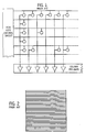
- Such an x-ray detector is illustrated by way of example in Fig. 3, where a 36 by 36 element detector array 100 is segmented into 36 regions 102. Each region 102 is a 6 row by 6 column sub-array of 36 detector elements as illustrated at 104.
- All of the detector elements in each region 102 connect through a common data line 105 to one of 36 pre-amplifiers 106, and each of the 36 detector elements in a region 102 connect to separate ones of 36 control lines 108 driven by a scan sequencer 110.
- Each of the regions 102 is associated with one data line 105 and one pre-amplifier 106, whereas each of the 36 control lines 108 is associated with the same corresponding detector element in each of the 36 regions 102.
- the detector array 100 can be scanned in a number of different ways.
- the particular scanning method used is determined by the operation of the scan sequencer 110.
- the detector array 100 can be scanned in a high resolution mode in which the 36 control lines 108 are sequentially enabled by the sequencer 110.
- one detector element in each sub-array 104 is read out to the pre-amplifier 106 associated with the element's region 102.
- one 36 by 36 pixel image may be produced.
- the detector array 100 can also be scanned faster at lower spatial resolutions.
- the scan sequencer 110 can drive four control lines at a time to read out four detector elements at the same time from each region 102.
- the control lines 108 are driven such that 4-element blocks of elements indicated by dashed line 112 are read out to each pre-amplifier 106.
- an 18 by 18 pixel image can be produced.
- the scan sequencer 110 can be operated to read out a 9-element block of elements as indicated by dashed line 114.
- a 12 by 12 pixel image can be produced. It can be appreciated by those skilled in the art that detector arrays 100 have many more detector elements and many more regions than that illustrated in Fig. 3. The size is limited in this example solely for the purpose of more clearly illustrating the invention.
- the present invention also enables the different regions 102 of the detector array 100 to be read out differently. For example, some of the regions 102 may be read out more often in a low spatial resolution mode, while other regions 102 are read out less often at a high spatial resolution mode.
- One application of this capability is to identify the regions 102 that lie within the patient being imaged and those regions that are background. The background regions 102 are scanned in a low resolution mode and the patient regions 102 are scanned at a higher resolution. This provides a number of benefits.
- the patient regions 102 are read at a slower rate which allows more time for the charges to accumulate on each detector element therein. This enables a higher SNR to be achieved in the clinically important regions of the image.
- the background regions 102 are read at a higher rate which prevents the charges on their detector elements from saturating the detectors and pre-amplifiers. Furthermore, since the low resolution background data is obtained at a higher rate, much of this data may be ignored, or dumped. This significantly reduces the processing burden on the x-ray system and enables an overall increase in time resolution for processor-bound systems.
- Another aspect of the present invention is the ability to measure the x-ray exposure from different regions of the image.
- the resolution of the measurement may range from that of a single detector element to that of an entire region 102.
- a prescan measures the exposure at different locations, and based on these measurements, the best spatial/contrast resolution for each of the regions 102 can be determined and used to program the scan sequencer 110.
- Such a prescan of the patient can be used to identify the clinical region of interest (such as a particular organ) and the resolution/contrast can be optimized for the corresponding regions 102.
- the programmed scan sequencer 110 then performs an image scan of the detector array 100 which is optimized to provide high resolution, high SNR images in the region of clinical interest.
- Yet another aspect of the present invention is the ability to reduce the cost of the imaging system. By configuring certain regions for high resolution imaging and other regions for low resolution imaging, available electronic hardware is more efficiently used. This enables less electronic hardware to be used for a given set of image quality specifications. In addition, the acquisition of excess data from regions such as the background may be reduced with a corresponding reduction in image reconstruction hardware and processing capability.
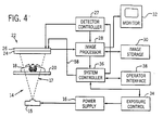
- an x-ray apparatus 14 includes an x-ray tube 15 which, when excited by a power supply 16, emits an x-ray beam 17. As illustrated, the x-ray beam is directed toward a patient 18 lying on an x-ray transmissive table 20. The portion of the beam which is transmitted through the table and the patient impinges upon an x-ray detector assembly 22.
- the x-ray detector assembly 22 comprises a scintillator 24 that converts the x-ray photons to lower energy photons in the visible spectrum. Contiguous with the scintillator 24 is an image photodetector array 26, which converts the light photons into an electrical signal.
- a detector controller 27 contains electronics for operating the detector array 26 to acquire an image and to read out the signal from each photodetector element.
- the output signal from the image photodetector array 26 is coupled to an image processor 28 that includes circuitry for collecting, processing and enhancing the x-ray image signal.
- the processed image is displayed on a video monitor 32 and may be stored in an image storage device 30.
- the overall operation of the x-ray apparatus 14 is governed by a system controller 36 which receives commands from the user via an operator interface panel 38.
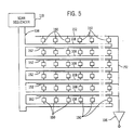
- the image photodetector array 26 consists of amorphous silicon devices on a glass substrate. It is constructed using well known techniques such as those disclosed in U.S. Pat. Nos. 5,041,888; 5,352,884 and 5,401, 668. To implement the present invention the separate detector elements are not interconnected in the row and column configurations as is done in prior systems. Instead, the detector elements are interconnected to form regions 102 as shown in Fig. 3. In the preferred embodiment the photodetector array 26 has 2048 by 2048 detector elements which are segmented into 4096 regions 102. Each region 102 has 32 by 32 detector elements which connect to a single region pre-amplifier 106. Each detector element has a size of 200 by 200 microns.
- the detector elements 150 are physically arranged in an array of columns and rows.
- a data line 152 connects to each detector element 150 in the region 102 and couples the data signals therefrom to the input of a region pre-amplifier 106.
- the pre-amplifier 106 amplifies the data signals to a level suitable for application to an analog-to-digital converter (not shown in the drawings).
- the detector elements 150 in each region 102 are each also connected to a separate control line in control line bus 108.
- the control lines 108 are driven by a scan sequencer 110 which is programmed to gate the signals from the detector elements 150 in a pattern determined by the specified scan being conducted.
- the gated detector element signal is conveyed through the data line 152 to the region pre-amplifier 106.
- a block of detector elements 150 can be gated simultaneously, in which case, their signals combine on the data line 152.
- each region 102 in the detector array 26 is connected in identical fashion to the control line bus 108. However, each region 102 has its own preamplifier 106. Consequently, corresponding detector elements 150 in each of the regions 102 are gated at the same moment by the scan sequencer 110, but their signals are captured by separate, corresponding region pre-amplifiers 106.
- additional scan sequencer circuitry can be added to readout selected regions 102 in the detector array 26 at differing rates.
- the detector array 26 can be configured to assign more than one scan sequencer to read out selected regions 102.
- two scan sequencers 110 assigned to different regions 102 are selectively connected to field effect transistor switches (not shown in the drawings) and the scan sequencer 110 then reads out the signal from a first set of detector element, or elements, to the preamplifier 106 at one rate and also reads out the signal from another set of detector element, or elements to the preamplifier 106 at an entirely different rate.
- Other circuit arrangements are also possible to configure particular scan sequencers and regions 102 differently.
- the scan sequencer 110 can be programmed to carry out a wide variety of different scans, or read outs, of the detector array 26.
- the scan sequencer 110 is programmed to sequentially gate each detector element 150, one at a time.
- Each detector element 150 thus provides a signal for a separate pixel in a reconstructed image having a resolution corresponding to the spacing between detector elements 150.
- Lower resolution images may be produced by programming the scan sequencer 110 to read out blocks of detector element signals. For example, blocks of four detector elements 150 may be read out onto the data line 152 to reduce the image resolution by one-half. However, only one-fourth the number of read out operations are required to do this, and as a result, the scan rate can be increased up to four times as fast. Larger blocks of detector elements 150 can also be read out to further reduce resolution and increase scan rate. In some applications it may even be advisable to read out all the detector elements 150 in the region 102 as a single block. For example, large blocks of detectors 150 may be read out during a calibration scan to operate an exposure control 34 or a variable exposure control across the entire image plane and to thereby adjust the x-ray tube dose rate.
- the present invention may be implemented in many different ways and used in many different clinical applications. It is particularly useful in clinical applications where the clinical region of interest occupies a relatively small portion of the entire image field of view. Such applications include, for example, pediatric images, organ and limb images, head images, and heart and tumor images.
Landscapes
- Engineering & Computer Science (AREA)
- Multimedia (AREA)
- Signal Processing (AREA)
- Measurement Of Radiation (AREA)
- Apparatus For Radiation Diagnosis (AREA)
- Transforming Light Signals Into Electric Signals (AREA)
Applications Claiming Priority (2)
| Application Number | Priority Date | Filing Date | Title |
|---|---|---|---|
| US09/407,350 US6437338B1 (en) | 1999-09-29 | 1999-09-29 | Method and apparatus for scanning a detector array in an x-ray imaging system |
| US407350 | 1999-09-29 |
Publications (1)
| Publication Number | Publication Date |
|---|---|
| EP1089555A1 true EP1089555A1 (en) | 2001-04-04 |
Family
ID=23611672
Family Applications (1)
| Application Number | Title | Priority Date | Filing Date |
|---|---|---|---|
| EP00308544A Withdrawn EP1089555A1 (en) | 1999-09-29 | 2000-09-28 | Method and apparatus for scanning a detector array in an x-ray imaging system |
Country Status (4)
| Country | Link |
|---|---|
| US (1) | US6437338B1 (enExample) |
| EP (1) | EP1089555A1 (enExample) |
| JP (1) | JP4717993B2 (enExample) |
| IL (1) | IL138357A0 (enExample) |
Cited By (8)
| Publication number | Priority date | Publication date | Assignee | Title |
|---|---|---|---|---|
| WO2003030521A1 (de) * | 2001-09-27 | 2003-04-10 | Conti Temic Microelectronic Gmbh | Bildaufnehmer, insbesondere zur dreidimensionalen erfassung von objekten oder szenen |
| EP1312938A2 (de) | 2001-11-17 | 2003-05-21 | Philips Intellectual Property & Standards GmbH | Anordnung von Strahlungs-Sensorelementen |
| WO2004032484A1 (en) * | 2002-10-01 | 2004-04-15 | Philips Intellectual Property & Standards Gmbh | Method and device for generating sub-images |
| FR2863435A1 (fr) * | 2003-12-08 | 2005-06-10 | Ge Med Sys Global Tech Co Llc | Detecteurs de rayons x a lignes de balayage divisees et lignes de donnees combinees |
| US7161154B2 (en) | 2003-01-16 | 2007-01-09 | Koninklijke Philips Electronics, N.V. | Array of sensor elements |
| EP2362641A1 (en) * | 2010-02-18 | 2011-08-31 | Raytheon Company | Imaging System |
| US8511823B2 (en) | 2010-02-18 | 2013-08-20 | Raytheon Company | Imaging system |
| US9277141B2 (en) | 2010-08-12 | 2016-03-01 | Raytheon Company | System, method, and software for image processing |
Families Citing this family (24)
| Publication number | Priority date | Publication date | Assignee | Title |
|---|---|---|---|---|
| DE19947536A1 (de) * | 1999-10-02 | 2001-04-05 | Philips Corp Intellectual Pty | Verfahren zum Auslesen der Sensorelemente eines Sensors sowie Sensor |
| DE10053934A1 (de) * | 2000-10-31 | 2002-05-08 | Philips Corp Intellectual Pty | Vorrichtung und Verfahren zum Auslesen eines in Bildpunkte unterteilten elektronischen Bildsensors |
| US6914227B2 (en) * | 2001-06-25 | 2005-07-05 | Canon Kabushiki Kaisha | Image sensing apparatus capable of outputting image by converting resolution by adding and reading out a plurality of pixels, its control method, and image sensing system |
| DE10160527A1 (de) * | 2001-12-10 | 2003-06-26 | Siemens Ag | Sensoranordnung mit Auslesemitteln zur Differenzbildung |
| US6963631B2 (en) * | 2002-10-25 | 2005-11-08 | Koninklijke Philips Electronics N.V. | Dynamic detector interlacing for computed tomography |
| DE10307752B4 (de) * | 2003-02-14 | 2007-10-11 | Siemens Ag | Röntgendetektor |
| US6859514B2 (en) * | 2003-03-14 | 2005-02-22 | Ge Medical Systems Global Technology Company Llc | CT detector array with uniform cross-talk |
| US7081628B2 (en) * | 2003-11-10 | 2006-07-25 | Ge Medical Systems Global Technology Company, Llc | Spatially patterned light-blocking layers for radiation imaging detectors |
| DE60318214T2 (de) | 2003-11-21 | 2008-12-18 | Carestream Health, Inc., Rochester | Zahnärztliches Röntgengerät |
| JP2007104219A (ja) * | 2005-10-03 | 2007-04-19 | Canon Inc | 放射線撮影装置及びその制御方法、放射線撮影システム |
| DE102005049228B4 (de) * | 2005-10-14 | 2014-03-27 | Siemens Aktiengesellschaft | Detektor mit einem Array von Photodioden |
| RU2473099C2 (ru) | 2007-05-16 | 2013-01-20 | Конинклейке Филипс Электроникс Н.В. | Виртуальный детектор рет и схема квазипикселированного считывания для рет |
| CN101655984B (zh) * | 2008-05-12 | 2015-02-18 | 美国西门子医疗解决公司 | 医学图像数据的自适应处理系统 |
| JP2010190830A (ja) * | 2009-02-20 | 2010-09-02 | Hamamatsu Photonics Kk | 放射線検出装置 |
| US8324586B2 (en) * | 2009-05-18 | 2012-12-04 | General Electric Company | Configurable multi resolution flat panel detector |
| US9262845B2 (en) | 2010-06-21 | 2016-02-16 | Koninklijke Philips N.V. | Image data reconstructed from undersampled higher resolution and incomplete lower resolution projection data |
| JP5617541B2 (ja) * | 2010-11-04 | 2014-11-05 | コニカミノルタ株式会社 | 放射線画像撮影装置 |
| KR101298913B1 (ko) | 2011-08-23 | 2013-08-20 | 한국전기연구원 | 광 스위칭 방식을 이용하는 디지털 엑스―선 영상 검출기의 스캔 방법 |
| US9013615B2 (en) | 2011-09-21 | 2015-04-21 | Semiconductor Components Industries, Llc | Image sensor with flexible interconnect capabilities |
| US9818182B2 (en) * | 2012-06-20 | 2017-11-14 | Hitachi, Ltd. | X-ray CT device |
| JP6561428B2 (ja) * | 2013-08-05 | 2019-08-21 | 株式会社ニコン | 電子機器、制御方法、及び制御プログラム |
| JP6274501B2 (ja) * | 2013-11-26 | 2018-02-07 | キヤノンメディカルシステムズ株式会社 | X線診断装置 |
| JP6342175B2 (ja) | 2014-02-10 | 2018-06-13 | キヤノンメディカルシステムズ株式会社 | X線ct装置 |
| JP6601465B2 (ja) * | 2017-08-15 | 2019-11-06 | 株式会社ニコン | 撮像装置 |
Citations (4)
| Publication number | Priority date | Publication date | Assignee | Title |
|---|---|---|---|---|
| US4339775A (en) * | 1980-06-16 | 1982-07-13 | Eastman Technology, Inc. | Fast frame rate augmentation |
| DE19524858A1 (de) * | 1995-07-07 | 1997-01-09 | Siemens Ag | Röntgenbilderzeugungssystem |
| GB2332585A (en) * | 1997-12-18 | 1999-06-23 | Simage Oy | Imaging array with controllable resolution |
| US5949483A (en) * | 1994-01-28 | 1999-09-07 | California Institute Of Technology | Active pixel sensor array with multiresolution readout |
Family Cites Families (10)
| Publication number | Priority date | Publication date | Assignee | Title |
|---|---|---|---|---|
| US4589770A (en) * | 1982-10-25 | 1986-05-20 | The Boeing Company | Electro-optical ranging apparatus having scanning circuitry and servoloop processor for resolving separation of images on photoelectric detector arrays |
| US4996413A (en) | 1990-02-27 | 1991-02-26 | General Electric Company | Apparatus and method for reading data from an image detector |
| US5352884A (en) | 1993-04-14 | 1994-10-04 | General Electric Corporation | Method and apparatus for providing offset for light detector |
| US5401668A (en) | 1993-09-02 | 1995-03-28 | General Electric Company | Method for fabrication solid state radiation imager having improved scintillator adhesion |
| BE1007803A3 (nl) * | 1993-11-26 | 1995-10-24 | Philips Electronics Nv | Beeldopneemapparaat. |
| AU1835397A (en) * | 1996-01-22 | 1997-08-22 | California Institute Of Technology | Active pixel sensor array with multiresolution readout |
| US6137151A (en) * | 1996-11-19 | 2000-10-24 | Xerox Corporation | Amorphous silicon sensor array with reduced number of address lines |
| US5877501A (en) | 1996-11-26 | 1999-03-02 | Picker International, Inc. | Digital panel for x-ray image acquisition |
| AU736265B2 (en) * | 1996-11-29 | 2001-07-26 | Varian Medical Systems, Inc. | Multiple mode digital X-ray imaging system |
| US5751783A (en) | 1996-12-20 | 1998-05-12 | General Electric Company | Detector for automatic exposure control on an x-ray imaging system |
-
1999
- 1999-09-29 US US09/407,350 patent/US6437338B1/en not_active Expired - Lifetime
-
2000
- 2000-09-10 IL IL13835700A patent/IL138357A0/xx active IP Right Grant
- 2000-09-28 EP EP00308544A patent/EP1089555A1/en not_active Withdrawn
- 2000-09-28 JP JP2000295357A patent/JP4717993B2/ja not_active Expired - Lifetime
Patent Citations (4)
| Publication number | Priority date | Publication date | Assignee | Title |
|---|---|---|---|---|
| US4339775A (en) * | 1980-06-16 | 1982-07-13 | Eastman Technology, Inc. | Fast frame rate augmentation |
| US5949483A (en) * | 1994-01-28 | 1999-09-07 | California Institute Of Technology | Active pixel sensor array with multiresolution readout |
| DE19524858A1 (de) * | 1995-07-07 | 1997-01-09 | Siemens Ag | Röntgenbilderzeugungssystem |
| GB2332585A (en) * | 1997-12-18 | 1999-06-23 | Simage Oy | Imaging array with controllable resolution |
Cited By (12)
| Publication number | Priority date | Publication date | Assignee | Title |
|---|---|---|---|---|
| WO2003030521A1 (de) * | 2001-09-27 | 2003-04-10 | Conti Temic Microelectronic Gmbh | Bildaufnehmer, insbesondere zur dreidimensionalen erfassung von objekten oder szenen |
| EP1312938A2 (de) | 2001-11-17 | 2003-05-21 | Philips Intellectual Property & Standards GmbH | Anordnung von Strahlungs-Sensorelementen |
| US6839407B2 (en) | 2001-11-17 | 2005-01-04 | Koninklijke Philips Electronics N.V. | Arrangement of sensor elements |
| WO2004032484A1 (en) * | 2002-10-01 | 2004-04-15 | Philips Intellectual Property & Standards Gmbh | Method and device for generating sub-images |
| CN100484192C (zh) * | 2002-10-01 | 2009-04-29 | 皇家飞利浦电子股份有限公司 | 用于生成子图像的方法和设备 |
| US7831109B2 (en) * | 2002-10-01 | 2010-11-09 | Koninklijke Philips Electronics N.V. | Method and device for generating sub-images |
| US7161154B2 (en) | 2003-01-16 | 2007-01-09 | Koninklijke Philips Electronics, N.V. | Array of sensor elements |
| FR2863435A1 (fr) * | 2003-12-08 | 2005-06-10 | Ge Med Sys Global Tech Co Llc | Detecteurs de rayons x a lignes de balayage divisees et lignes de donnees combinees |
| US7119341B2 (en) | 2003-12-08 | 2006-10-10 | General Electric Company | Split scan line and combined data line x-ray detectors |
| EP2362641A1 (en) * | 2010-02-18 | 2011-08-31 | Raytheon Company | Imaging System |
| US8511823B2 (en) | 2010-02-18 | 2013-08-20 | Raytheon Company | Imaging system |
| US9277141B2 (en) | 2010-08-12 | 2016-03-01 | Raytheon Company | System, method, and software for image processing |
Also Published As
| Publication number | Publication date |
|---|---|
| US6437338B1 (en) | 2002-08-20 |
| JP2001174565A (ja) | 2001-06-29 |
| IL138357A0 (en) | 2001-10-31 |
| JP4717993B2 (ja) | 2011-07-06 |
Similar Documents
| Publication | Publication Date | Title |
|---|---|---|
| US6437338B1 (en) | Method and apparatus for scanning a detector array in an x-ray imaging system | |
| EP0844588B1 (en) | Image processing apparatus and method | |
| US5142557A (en) | CCD and phosphor screen digital radiology apparatus and method for high resolution mammography | |
| US7514663B2 (en) | Imaging apparatus having a read out circuit unit with dual readout operation and method of improving a frame rate | |
| CN103126695B (zh) | 放射线照相图像检测器及其控制方法 | |
| CN100536773C (zh) | 放射线成像系统及其驱动方法 | |
| US7016461B2 (en) | Real-time digital x-ray imaging apparatus | |
| CN101120246B (zh) | 多模式平板x射线成像系统及方法 | |
| US5773832A (en) | Advanced CCD-based x-ray image sensor system | |
| JP3647440B2 (ja) | X線撮影装置 | |
| JPH08257026A (ja) | デジタルx線撮影装置 | |
| WO2009102839A2 (en) | Imaging array data acquisition system and use thereof | |
| US6973160B2 (en) | X-ray-tomographic imaging apparatus, X-ray-tomographic imaging method, and program | |
| US6243440B1 (en) | Radiographic apparatus | |
| JP2004057816A (ja) | 交互配置型走査線を備えた固体検出器を用いて一連の画像を取得する方法及び装置 | |
| JP2001189891A (ja) | センサのセンサ要素を読み出す方法及びセンサ | |
| US5027380A (en) | Diagnostic X-ray apparatus | |
| US7122802B2 (en) | Method and apparatus for increasing the data acquisition rate in a digital detector | |
| JPH09289985A (ja) | X線画像表示方法及び装置 | |
| KR100788082B1 (ko) | 엑스레이 진단 장치 및 엑스레이 진단 장치를 제어하는 방법 | |
| JPH07312297A (ja) | X線診断装置 | |
| JP2002250772A (ja) | 撮像装置及び撮像方法 | |
| JPH11128214A (ja) | X線診断装置 | |
| JP3369441B2 (ja) | 多方向x線透視撮影装置 | |
| US5006709A (en) | X-ray diagnostics installation |
Legal Events
| Date | Code | Title | Description |
|---|---|---|---|
| PUAI | Public reference made under article 153(3) epc to a published international application that has entered the european phase |
Free format text: ORIGINAL CODE: 0009012 |
|
| AK | Designated contracting states |
Kind code of ref document: A1 Designated state(s): DE NL |
|
| AX | Request for extension of the european patent |
Free format text: AL;LT;LV;MK;RO;SI |
|
| 17P | Request for examination filed |
Effective date: 20011004 |
|
| AKX | Designation fees paid |
Free format text: DE NL |
|
| 17Q | First examination report despatched |
Effective date: 20071221 |
|
| STAA | Information on the status of an ep patent application or granted ep patent |
Free format text: STATUS: THE APPLICATION IS DEEMED TO BE WITHDRAWN |
|
| 18D | Application deemed to be withdrawn |
Effective date: 20160401 |