EP1089345A2 - Lateraler Leistungsfeldeffekttransistor - Google Patents
Lateraler Leistungsfeldeffekttransistor Download PDFInfo
- Publication number
- EP1089345A2 EP1089345A2 EP00308356A EP00308356A EP1089345A2 EP 1089345 A2 EP1089345 A2 EP 1089345A2 EP 00308356 A EP00308356 A EP 00308356A EP 00308356 A EP00308356 A EP 00308356A EP 1089345 A2 EP1089345 A2 EP 1089345A2
- Authority
- EP
- European Patent Office
- Prior art keywords
- conductivity
- type
- region
- well
- interval
- Prior art date
- Legal status (The legal status is an assumption and is not a legal conclusion. Google has not performed a legal analysis and makes no representation as to the accuracy of the status listed.)
- Granted
Links
Images









Classifications
-
- H—ELECTRICITY
- H10—SEMICONDUCTOR DEVICES; ELECTRIC SOLID-STATE DEVICES NOT OTHERWISE PROVIDED FOR
- H10D—INORGANIC ELECTRIC SEMICONDUCTOR DEVICES
- H10D62/00—Semiconductor bodies, or regions thereof, of devices having potential barriers
- H10D62/10—Shapes, relative sizes or dispositions of the regions of the semiconductor bodies; Shapes of the semiconductor bodies
- H10D62/13—Semiconductor regions connected to electrodes carrying current to be rectified, amplified or switched, e.g. source or drain regions
- H10D62/149—Source or drain regions of field-effect devices
- H10D62/151—Source or drain regions of field-effect devices of IGFETs
- H10D62/156—Drain regions of DMOS transistors
- H10D62/157—Impurity concentrations or distributions
-
- H—ELECTRICITY
- H10—SEMICONDUCTOR DEVICES; ELECTRIC SOLID-STATE DEVICES NOT OTHERWISE PROVIDED FOR
- H10D—INORGANIC ELECTRIC SEMICONDUCTOR DEVICES
- H10D30/00—Field-effect transistors [FET]
- H10D30/60—Insulated-gate field-effect transistors [IGFET]
- H10D30/64—Double-diffused metal-oxide semiconductor [DMOS] FETs
- H10D30/65—Lateral DMOS [LDMOS] FETs
-
- H—ELECTRICITY
- H10—SEMICONDUCTOR DEVICES; ELECTRIC SOLID-STATE DEVICES NOT OTHERWISE PROVIDED FOR
- H10D—INORGANIC ELECTRIC SEMICONDUCTOR DEVICES
- H10D62/00—Semiconductor bodies, or regions thereof, of devices having potential barriers
- H10D62/10—Shapes, relative sizes or dispositions of the regions of the semiconductor bodies; Shapes of the semiconductor bodies
- H10D62/124—Shapes, relative sizes or dispositions of the regions of semiconductor bodies or of junctions between the regions
- H10D62/126—Top-view geometrical layouts of the regions or the junctions
- H10D62/127—Top-view geometrical layouts of the regions or the junctions of cellular field-effect devices, e.g. multicellular DMOS transistors or IGBTs
-
- H—ELECTRICITY
- H10—SEMICONDUCTOR DEVICES; ELECTRIC SOLID-STATE DEVICES NOT OTHERWISE PROVIDED FOR
- H10D—INORGANIC ELECTRIC SEMICONDUCTOR DEVICES
- H10D62/00—Semiconductor bodies, or regions thereof, of devices having potential barriers
- H10D62/10—Shapes, relative sizes or dispositions of the regions of the semiconductor bodies; Shapes of the semiconductor bodies
- H10D62/13—Semiconductor regions connected to electrodes carrying current to be rectified, amplified or switched, e.g. source or drain regions
- H10D62/149—Source or drain regions of field-effect devices
- H10D62/151—Source or drain regions of field-effect devices of IGFETs
- H10D62/156—Drain regions of DMOS transistors
- H10D62/159—Shapes
-
- H—ELECTRICITY
- H10—SEMICONDUCTOR DEVICES; ELECTRIC SOLID-STATE DEVICES NOT OTHERWISE PROVIDED FOR
- H10D—INORGANIC ELECTRIC SEMICONDUCTOR DEVICES
- H10D62/00—Semiconductor bodies, or regions thereof, of devices having potential barriers
- H10D62/10—Shapes, relative sizes or dispositions of the regions of the semiconductor bodies; Shapes of the semiconductor bodies
- H10D62/102—Constructional design considerations for preventing surface leakage or controlling electric field concentration
- H10D62/103—Constructional design considerations for preventing surface leakage or controlling electric field concentration for increasing or controlling the breakdown voltage of reverse-biased devices
- H10D62/105—Constructional design considerations for preventing surface leakage or controlling electric field concentration for increasing or controlling the breakdown voltage of reverse-biased devices by having particular doping profiles, shapes or arrangements of PN junctions; by having supplementary regions, e.g. junction termination extension [JTE]
-
- H—ELECTRICITY
- H10—SEMICONDUCTOR DEVICES; ELECTRIC SOLID-STATE DEVICES NOT OTHERWISE PROVIDED FOR
- H10D—INORGANIC ELECTRIC SEMICONDUCTOR DEVICES
- H10D62/00—Semiconductor bodies, or regions thereof, of devices having potential barriers
- H10D62/10—Shapes, relative sizes or dispositions of the regions of the semiconductor bodies; Shapes of the semiconductor bodies
- H10D62/13—Semiconductor regions connected to electrodes carrying current to be rectified, amplified or switched, e.g. source or drain regions
- H10D62/149—Source or drain regions of field-effect devices
- H10D62/151—Source or drain regions of field-effect devices of IGFETs
-
- H—ELECTRICITY
- H10—SEMICONDUCTOR DEVICES; ELECTRIC SOLID-STATE DEVICES NOT OTHERWISE PROVIDED FOR
- H10D—INORGANIC ELECTRIC SEMICONDUCTOR DEVICES
- H10D62/00—Semiconductor bodies, or regions thereof, of devices having potential barriers
- H10D62/10—Shapes, relative sizes or dispositions of the regions of the semiconductor bodies; Shapes of the semiconductor bodies
- H10D62/17—Semiconductor regions connected to electrodes not carrying current to be rectified, amplified or switched, e.g. channel regions
- H10D62/351—Substrate regions of field-effect devices
- H10D62/357—Substrate regions of field-effect devices of FETs
- H10D62/364—Substrate regions of field-effect devices of FETs of IGFETs
Definitions
- the present invention relates generally to a high voltage semiconductor device, and more particularly to a high voltage lateral power semiconductor device for a switching power supply, a motor drive, a fluorescent inverter drive and the like.
- PWM control method has become widespread for a switching power supply, a motor drive and a fluorescent inverter drive.
- a control circuit With respect to a control circuit, there is the need for improving the function, reducing the size and cost, improving the reliability and reducing the electricity consumption. Accordingly, there is an increasing demand for a power IC in which high voltage power elements are integrated.
- a power IC for a power supply which drives commercial 100-200V, requires an element breakdown voltage of 700V in order to drive a transformer.
- the power IC must be lateral and its substrate and drift region has a high resistivity (a low impurity concentration) (Journal of Electricity EDD-93-21, P21-29, Toshihiko Uno et al.
- Figure 18 is a plan view of a conventional high voltage lateral power semiconductor device as a first example
- Figure 8 is a cross-sectional view taken along line A-B of Figure 18.
- this semiconductor device is constructed in such a manner that an N well 2 and a P base 3 are formed on a p type substrate with a high resistivity of about 150 ⁇ cm.
- the N well 2 has a surface impurity concentration of 1x10 16 /cm 3 , and a diffusion depth of 6 ⁇ m.
- the amount of donor in the N well 2 is 1x10 12 /cm 2 .
- the total amount of donor in the N well, the resistivity of the P substrate and the distance of the drift region are optimised to achieve a high breakdown voltage.
- the P base which forms a source region, has a surface concentration of 3x10 16 /cm 3 , and a diffusion depth of 6 ⁇ m.
- a threshold voltage of a power MOS is determined according to the surface concentration. Then, a thermal oxide film 4 with a thickness of 0.6 ⁇ m, and a polysilicon gate 6 is formed through a gate oxide film 5 of 25nm.
- n + diffused layer with a surface concentration of 1x10 20 /cm 3 , and a diffusion depth of 0.2 ⁇ m is formed in a source 7 and a drain 8, and a contact P + diffused layer (with a surface concentration of 5x10 19 /cm 3 , and a diffusion depth of 0.5 ⁇ m) 9 is formed on the surface of the P base.
- An interlayer insulating film 10 is formed and a contact hole 11 is opened, and then a source electrode 12 and a drain (gate) electrode 13 are formed.
- the device is shaped like the teeth of a comb having a straight portion 20 in which the P base region 3 forming the source region and the drain 8 are parallel to one another if they are viewed prospectively, and corner parts 21, 22 having the same interval between the P base region 2 and the drain 8 as the parallel interval of the straight portion 20.
- a channel width must be not less than 50mm and the number of teeth of the comb must be more than 10 and less than 20.
- the straight portion 20 and an end portion of the teeth of a comb pattern at the corner part have the cross-sectional structure shown in Figure 19.
- the breakdown voltage is 800V. If, however, radius of curvature is 12.5 ⁇ m, the electric fields are heavily concentrated at the corner part. This lowers the breakdown voltage to 600V. Therefore, the radius of curvature must be not less than 50 ⁇ m in order to ensure the breakdown voltage of 700V. More specifically, a device pitch cannot be reduced, and it is therefore impossible to improve the current driving performance per unit area. Accordingly, the breakdown voltage of the power semiconductor device is 700V and the ON resistance per unit area is about 90 ⁇ /mm 2 in this prior art.
- Figure 20 is a cross-sectional view of a conventional high voltage lateral power semiconductor device as a second example. A plan view thereof is the same as Figure 18.
- an N well 2A is formed on a p type substrate 1 with a high resistivity of about 150 ⁇ cm, and a P base 3A is formed inside the N well 2A.
- the N well 2A has a surface impurity concentration of 1x10 16 /cm 3 , and a diffusion depth of 6 ⁇ m.
- the amount of donor in the N well 2A is 1x10 12 /cm 2 .
- the total amount of donor in the N well 2A, the resistivity of the P substrate 1 and the distance of the drift region are optimised to achieve a high breakdown voltage.
- the P base 3A has a surface concentration of 3x10 16 /cm 3 , and a diffusion depth of 2 ⁇ m.
- a threshold voltage of a power MOS is determined according to the surface concentration.
- a p type surface region 14 is formed between the P base 3A and an n + drain.
- the p type surface region 14 has a surface impurity concentration of 5x10 16 /cm 3 , and a diffusion depth of 1 ⁇ m.
- a straight portion and a corner part 22A at an end portion of the teeth of the comb have the cross-sectional structure shown in Figure 20.
- the breakdown voltage is 800V.
- radius of curvature is 12.5 ⁇ m, the electric fields are heavily concentrated at the corner part. This lowers the breakdown voltage to 600V.
- the radius of curvature cannot be reduced to not less than 50 ⁇ m in order to ensure the breakdown voltage of 700V.
- the device pitch cannot be reduced, and it is therefore impossible to improve the current driving performance per unit area. Accordingly, the ON resistance per unit area is as high as 60 ⁇ /mm 2 if the radius of curvature is set at 50 ⁇ m in order to ensure the breakdown voltage of 700V.
- a semiconductor device of the third example in which a drain corner part has an electric field reliving structure as disclosed in Japanese Patent Provisional Publication No. 6-244412.
- Figure 21 is a plan view showing a prior art of the third example
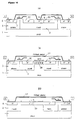
- Figure 11 is a partial cross-sectional view showing a principal part of Figure 2.
- Figure 22(a) is a cross-sectional view taken along line A-B of Figure 21
- Figure 22(b) is a cross-sectional view taken along line C-D of Figure 21
- Figure 22(c) is a cross-sectional view taken along line E-F of Figure 21.
- the end portion 22A at the drain corner part in Figure 18 is shortened as shown in Figure 21, and the p type surface region 14 in this region is eliminated by a length L and a width W to form an n type surface region 16.
- the width W of the eliminated region is optimised to thereby relieve the electric fields at the corner part.
- the relief of the electric fields must be adjusted within the width of the p type surface region 14 in the N well 2A at the drain corner end portion. Since the N well 2A has a relatively high surface impurity concentration, the range of optimum values of the width W is very narrow and this increases the dispersion in the breakdown voltage. For this reason, the radius of curvature needs to be 30 ⁇ m in order to ensure the breakdown voltage of 700V, and thus, the ON resistance per unit area is lowered by only 15%. It is therefore impossible to satisfactorily lower the ON resistance.
- the conventional semiconductor devices have disadvantages because the electric fields are concentrated at the corner part and the breakdown voltage cannot be sustained if the integration degree is improved for the purpose of improving the current driving performance. It is therefore difficult to improve the current driving performance by improving the integration degree.
- a semiconductor device which broadens the interval in a voltage applied region at a corner part, provides a region with an optimised impurity concentration in that part, and fills a depletion layer to thereby relieve the concentration of electric fields.
- the present invention is directed to a semiconductor device, in which a second-conductivity-type well is formed on a first-conductivity-type semiconductor substrate and a second-conductivity-type diffused region is formed inside the well, and in which a first-conductivity-type diffused region is formed at a desired position on the first-conductivity-type semiconductor substrate, the first-conductivity-type diffused region and the second-conductivity-type diffused region having straight portions with a uniform interval, a corner part being formed at an end portion of the straight portions, the semiconductor device characterised in that: at the corner part in the second-conductivity-type diffused region, the interval between the first-conductivity-type diffused region and the second-conductivity-type diffused region is larger than the interval between the straight portions, and the conductivity characteristics in a larger interval region are different from those of the second-conductivity-type well along a predetermined width in order to relieve concentration of electric fields at the corner part.
- This arrangement relieves the concentration of electric fields at the corner part and the like, and therefore easily improves the current driving performance by improving the integration degree.
- a first-conductivity-type region is formed along a predetermined width in the interval region.
- the first-conductivity-type semiconductor substrate can be used as the first-conductivity-type region in the interval region, and this extremely simplifies the structure by eliminating the necessity of adding any impurities.
- the high-resistivity first-conductivity-type semiconductor substrate is used as the first-conductivity-region in the depletion layer, and this enables the uniform relief of the electric fields to obtain an optimum value of the interval region in a relatively wide range. This makes it possible to easily adjust the relief of the electric fields.
- a second-conductivity-type region is formed along a predetermined width in the interval region, the second-conductivity-type region having a different impurity concentration from that of the second-conductivity-type well.
- the depletion layer can be spread by adjusting the impurity concentration of the second-conductivity-region, and this enables the uniform relief of the electric fields and achieves the high breakdown voltage.
- the n type second-conductivity-region is formed of phosphorous P
- the phosphorous is deposited on an interface of an oxide film and a silicon substrate by thermal treatment, and therefore, the surface of the substrate has a high concentration.
- the surface can be composed of high-concentration n type impurities, and this controls the shift in the breakdown voltage caused by plus electric charge generated inside the oxide film and on the surface of the device.
- a second-conductivity-type region and a first-conductivity-type surface layer formed thereon are formed along a predetermined width in the interval region, the second-conductivity-type region having a different impurity concentration from the second-conductivity-type well along a predetermined width.
- This arrangement achieves the high impurity concentration of each conductivity-type region, and controls the shift in the breakdown voltage caused by the plus electric charge.
- a plurality of first-conductivity-type regions and second-conductivity-type regions is formed along a predetermined width in the interval region.
- This arrangement achieves the high impurity concentration of each conductivity-type region, and controls the shift in the breakdown voltage caused by the plus electric charge.
- a first-conductivity-type diffused surface layer is formed on a surface of the second-conductivity-type well.
- the amount of impurities is increased in the second-conductivity-type well. This reduces a drift resistance if the device has a high breakdown voltage.
- a second-conductivity-type region and a first-conductivity-type surface layer formed thereon are formed along a predetermined width in the interval region, the second-conductivity-type region having a different impurity concentration from the second-conductivity-type well along a predetermined width.
- the impurity concentration of the second-conductivity-type well can be increased to thereby reduce the drift resistance of the second-conductivity-type well if the device has a high breakdown voltage.
- the impurity concentration of the second-conductivity-type region and the first-conductivity-type surface layer can be increased to thereby to control the shift in the breakdown voltage caused by the plus electric charge.
- the first-conductivity-type diffused region and the second-conductivity-type diffused region are opposite to one another and form the teeth of a comb pattern, and the corner part is formed at an end portion of the teeth of the comb pattern.
- This arrangement broadens a channel width, and increases the current driving performance.
- the first-conductivity-type diffused region is formed inside the second-conductivity-type well.
- the impurity concentration of the drain region adjacent to a channel can be increased when a MOSFET is formed. This reduces a drain resistance.
- the first-conductivity-type diffused region is formed outside the second-conductivity-type well.
- This arrangement increases a channel length to thereby control the operation of parasitic bipolar transistors provided between the N well, the P base and the source.
- a second-conductivity-type source region is formed inside the first-conductivity-type region, and the second-conductivity-type diffused region formed inside the second-conductivity-type well is a MOSFET that functions as a drain region.
- This arrangement makes it possible to relieve the concentration of electric fields generated at the corner part and the like even if the integration degree of the device is improved. This realises a high voltage MOSFET device that is capable of easily improving the current driving performance by improving the integration degree.
- an N well as a second-conductivity-type well is formed on a p type substrate as a first-conductivity-type semiconductor substrate.
- a first-conductivity-type diffused region is formed as a p base outside the well, and a second-conductivity-type diffused region is formed as a drain inside the well.
- the first-conductivity-type diffused region and the second-conductivity-type diffused region are shaped like the teeth of a comb.
- the interval between the first-conductivity-type diffused region and the second-conductivity-type diffused region in a part where the second-conductivity-type forms an end portion of the teeth of the comb is larger than the interval in other straight portions.
- the second-conductivity-type well at the end portion is partially formed as a first-conductivity-type region.
- Figure 1 is a plan view showing the first embodiment of the present invention
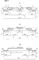
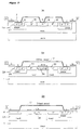
- Figure 2 is a cross-sectional view showing some parts of Figure 1 wherein Figure 2(a) is a cross-sectional view taken along line A-B of Figure 1, Figure 2(b) is a cross-sectional view taken along line C-D, and Figure 2(c) is a cross-sectional view taken along line E-F.
- an N well 2 and a P base 3 are formed on a high resistivity of about 150 ⁇ cm as shown in Figure 2(a).
- the N well 2 has a surface concentration of 1x10 16 /cm 3 , and a diffusion depth of 6 ⁇ m.
- the amount of donor in the N well is 1x10 12 /cm 2 .
- the amount of donor in the N well 2, the resistivity of a P type substrate 1, the distance of drift regions are optimised to achieve a high voltage.
- the P type substrate 1 has an impurity concentration of 1x10 14 /cm 3
- the P base 3 has a surface concentration of 3x10 16 /cm 3 and a diffusion depth of 6 ⁇ m.
- a threshold voltage of a power MOS is determined according to the surface concentration.
- a thermal oxide film 4 with a thickness of 0.6 ⁇ m, and a polysilicon gate 6 is formed through a gate oxide film 5 of 25nm.
- n + diffusion layer with a surface concentration of 1x10 20 /cm 3 and a diffusion depth of 0.2 ⁇ m is formed in a source 7 and a drain 8, and a contact p + diffusion layer 9 (with a surface concentration of 5x10 19 /cm 3 and a diffusion depth of 0.5 ⁇ m) is formed on a surface of the p base 3 to thereby form an interlayer insulating film.
- a source electrode 12 and a drain electrode 13 are formed after a contact hole 11 is opened.
- the source and drain electrodes are shaped like the teeth of a comb in order to improve a current driving performance. If there is a need for an actual output current capacity of 2-5A class, a channel width must be not less than 50mm and the number of teeth of the comb is more than 10 and less than 20.
- the p base 3 (the first-conductivity-type diffused region) and the drain (the second-conductivity-type diffused region) have a straight portion 20 with uniform interval, and corner parts 21, 22 are formed at an end portion of the straight portion 20.
- a drain corner part 22B has an electronic field relieving structure.
- the interval between the p base 3 and the drain 8 at the drain corner part 22B is larger than the interval in the other straight portions, and the conductivity characteristics of the N well 2 are partially different in a region with the larger interval.
- the N well of the prior art shown in Figure 18 is eliminated along a length L1 and a width W1, and the width W1 in the eliminated region (the region with the larger interval) is optimised to relieve the electric field at the corner part according to the first embodiment.
- the eliminated region is a p type region (a p type substrate of a first-conductivity-type) 31, and a field plate 17 extending from the drain electrode covers the end portion in such a way as to reach the N well 2 at the end portion.
- a depletion layer spreads in the p type substrate 1, which appears due to the elimination of the N well). Since the P type substrate 1 has a high resistivity, the electric field can be relieved uniformly and an optimum value of W1 can be determined in a relatively wide range in the achievement of the high voltage.
- L1 was fixed at 50 ⁇ m, and W1 was subject to change.
- the breakdown voltage of the corner part depends on W1. If W1 was 25 ⁇ m, the breakdown voltage was 770V. At this time, the radius of curvature at the drain corner part 22 is 12.5 ⁇ m. This structure reduces a device pitch and lowers an ON resistance per unit area by 40%.
- the p type substrate 1 is used for the region (a p type region 31) with the width W1; however, a p type region with a different concentration may be used instead of the p type substrate 1. Needless to say, the optimum values of W1 and the diffusion depth are different according to the concentration.
- p type region 31 can selectively add implant p type impurities into the N well 2. For example, p type ions are implanted into a lower section of a field oxide film in order to isolate elements in a low-voltage element part.
- an N well as a second-conductivity-type well is formed on a p type substrate as a first-conductivity-type semiconductor substrate.
- a first-conductivity-type diffused region as a p base is formed outside the well, and a second-conductivity-type diffused region as a drain is formed inside the well.
- the first-conductivity-type diffused region and the second-conductivity-type diffused region are shaped like the teeth of a comb.
- the interval between the first-conductivity-type diffused region and the second-conductivity-type diffused region in a part where the second-conductivity-type forms an end portion of the teeth of the comb is larger than the interval in other straight portions.
- the second-conductivity-type well at the end portion is partially formed as a first-conductivity-type region.
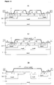
- Figure 3 is a cross-sectional view showing a principal part of the second embodiment.
- the plan view of the second embodiment is the same as Figure 1.
- the second embodiment is different from the first embodiment in that an N well 2b covers the whole source region (a P base 3B) as shown in Figure 3.
- the P base 3B is shallow with a depth of 2 ⁇ m.
- the other structure of the second embodiment is the same as the first embodiment, and a description thereof will not be given here.
- the above structure is characterised in that the double diffusion is performed by using a P base and an n + source whose mask is a polysilicon gate to thereby shorten a channel length.
- an N well as a second-conductivity-type well is formed on a p type substrate as a first-conductivity-type semiconductor substrate.
- a first-conductivity-type diffused region as a p base is formed outside the well, and a second-conductivity-type diffused region as a drain is formed inside the well.
- the first-conductivity-type diffused region and the second-conductivity-type diffused region are shaped like the teeth of a comb.
- the interval between the first-conductivity-type diffused region and the second-conductivity-type diffused region in a part where the second-conductivity-type diffused region forms an end portion of the teeth of the comb is larger than the interval in other straight portions.
- the second-conductivity-type well at the end portion is partially formed as a second-conductivity-type region with a different impurity concentration from that of the N well.
- Figure 4 is a cross-sectional view showing a principal part of the third embodiment.
- the plan view of the third embodiment is the same as Figure 1.
- the third embodiment is different from the first embodiment in that the N well 2 with the larger interval (the drain corner end portion as shown in Figure 18) is formed along a length L3 and a width W3 as an n type region 32 having a different impurity concentration from that of the N well 2. Otherwise, the third embodiment has the same structure as the first embodiment.
- the optimum value of the width W3 differs according to the amount of impurities in the n type region 32 and the concentration of the p type substrate.
- the n type region has an impurity concentration of 5x10 15 /cm 3 for example.
- the diffusion depth of the n type region is the same as that of the N well 2; however, it is needless to say that the diffusion depth of the n type region may be different from that of the N well 2.
- an n type well as a second-conductivity-type well is formed on a p type substrate as a first-conductivity-type semiconductor substrate.
- a P base as a first-conductivity-type diffused region is formed inside the well, and a drain as a second-conductivity-type diffused region is formed inside the well.
- the first-conductivity-type diffused region and the second-conductivity-type diffused region are shaped like the teeth of a comb.
- the interval between the first-conductivity-type diffused region and the second-conductivity-type diffused region in a part where the second-conductivity-type diffused region forms an end portion of the teeth of the comb is larger than the interval in other straight portions.
- the second-conductivity-type well at the end portion is partially formed as a second-conductivity-type region with a different impurity concentration from that of the N well.
- Figure 5 is a cross-sectional view showing a principal part of the fourth embodiment. A plan view thereof is the same as Figure 1.
- the fourth embodiment is different from the third embodiment in that an N well 2B covers a source region (P base 3B). Therefore, the P base 3B has a shallow depth of 2 ⁇ m. Otherwise, the fourth embodiment has the same structure as the first embodiment.
- an N well as a second-conductivity-type well is formed on a p type substrate as a first-conductivity-type semiconductor substrate.
- a P base as a first-conductivity-type diffused region is formed outside the well, and a drain as a second-conductivity-type diffused region is formed inside the well.
- the first-conductivity-type diffused region and the second-conductivity-type diffused region are shaped like the teeth of a comb.
- the interval between the first-conductivity-type diffused region and the second-conductivity-type diffused region in a part where the second-conductivity-type diffused region forms an end portion of the teeth of the comb is larger than the interval in other straight portions.
- the second-conductivity-type well at the end portion is partially formed as a second-conductivity-type region and a first-conductivity-type surface layer with a different impurity concentration from that of the N well.
- Figure 6 is a cross-sectional view showing a principal part of the fifth embodiment. A plan view thereof is the same as Figure 1.
- the fifth embodiment is different from the first embodiment in that the N well 2 in the interval region is formed along a length L5 and a width W5 as an n type region 33 with a different impurity concentration from that of the N well 2 and a p type region 34 (the first-conductivity-type surface layer) formed at the top of the n type region 33.
- the total diffusion depth of the n type region 33 and the p type region 34 is the same as the diffusion depth of the N well, but it is needless to say that the diffusion depth of the n type region 33 and the p type region 34 varies according to the concentration thereof.
- the fifth embodiment has substantially the same structure as the fifth embodiment. In this case, the optimum value of the width W5 varies according to the amount of impurities in the p type region 34 and the concentration of the p type substrate 1.
- the width W5 is 2.5 ⁇ m
- the impurity concentration of the p type region is 5x10 16 /cm 3
- the impurity concentration of the n type region is 3x10 16 /cm 3 .
- an N well as a second-conductivity-type well is formed on a p type substrate as a first-conductivity-type semiconductor substrate.
- a P base as a first-conductivity-type diffused region is formed inside the well, and a drain as a second-conductivity-type diffused region is formed inside the well.
- the first-conductivity-type diffused region and the second-conductivity-type diffused region are shaped like the teeth of a comb.
- the interval between the first-conductivity-type diffused region and the second-conductivity-type diffused region in a part where the second-conductivity-type diffused region forms an end portion of the teeth of the comb is larger than the interval in other straight portions.
- the second-conductivity-type well at the end portion is partially formed as a second-conductivity-type region and a first-conductivity-type surface layer with a different impurity concentration from that of the N well.
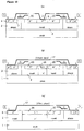
- Figure 7 is a cross-sectional view showing a principal part of the sixth embodiment. A plan view thereof is the same as Figure 1.
- the sixth embodiment is different from the fifth embodiment in that the N well 2B covers the whole source region (P base 3B). Therefore, the P base 3B has a shallow depth of 2 ⁇ m. Otherwise, the sixth embodiment has the same structure as the fifth embodiment, and a description thereof will not be given here.
- an N well as a second-conductivity-type well is formed on a p type substrate as a first-conductivity-type semiconductor substrate.
- a P base as a first-conductivity-type diffused region is formed outside the well, and a drain as a second-conductivity-type diffused region is formed inside the well.
- the first-conductivity-type diffused region and the second-conductivity-type diffused region are shaped like the teeth of a comb.
- the interval between the first-conductivity-type diffused region and the second-conductivity-type diffused region in a part where the second-conductivity-type diffused region forms an end portion of the teeth of the comb is larger than the interval in other straight portions.
- the second-conductivity-type well at the end portion is partially formed as a plurality of first-conductivity-type regions and second-conductivity-type regions.
- Figure 8 is a cross-sectional view showing a principal part of the seventh embodiment. A plan view thereof is the same as Figure 1.
- the N well 2 in the increased interval region is formed along a length L7 and a width W7 as a region 35 where a plurality of long and narrow p type and n type impurity regions are formed alternately.
- the width W7 is 25 ⁇ m
- the impurity concentration of the p type and n type impurity regions is 1x10 16 /cm 3 .
- an N well as a second-conductivity-type well is formed on a p type substrate as a first-conductivity-type semiconductor substrate.
- a P base as a first-conductivity-type diffused region is formed inside the well, and a drain as a second-conductivity-type diffused region is formed inside the well.
- the first-conductivity-type diffused region and the second-conductivity-type diffused region are shaped like the teeth of a comb.
- the interval between the first-conductivity-type diffused region and the second-conductivity-type diffused region in a part where the second-conductivity-type diffused region forms an end portion of the teeth of the comb is larger than the interval in other straight portions.
- the second-conductivity-type well at the end portion is partially formed as a plurality of first-conductivity-type regions and second-conductivity-type regions.
- Figure 9 is a cross-sectional view showing a principal part of the eighth embodiment. A plan view thereof is the same as Figure 1.
- the eighth embodiment is different from the seventh embodiment in that the N well 2B covers the whole source region (P base 3B). Therefore, the P base 3B has a shallow depth of 2 ⁇ m. Otherwise, the eighth embodiment has the same structure as the seventh embodiment.
- an N well as a second-conductivity-type well is formed on a p type substrate as a first-conductivity-type semiconductor substrate.
- a P base as a first-conductivity-type diffused region is formed outside the well, and a drain as a second-conductivity-type diffused region is formed inside the well.
- a first-conductivity-type diffused surface layer is formed on the surface of the well. The first-conductivity-type diffused region and the second-conductivity-type diffused region are shaped like the teeth of a comb.
- the interval between the first-conductivity-type diffused region and the second-conductivity-type diffused region in a part where the second-conductivity-type diffused region forms an end portion of the teeth of the comb is larger than the interval in other straight portions.
- the second-conductivity-type well at the end portion is partially formed as a first-conductivity-type region.
- Figure 10 is a cross-sectional view showing a principal part of the ninth embodiment. A plan view thereof is the same as Figure 1.
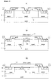
- a P base 3 is formed outside an N well 2, and a p type surface layer (the first-conductivity-type diffused surface layer) 30 is provided between the P base 3 and an n + drain 8 as shown in Figure 10(a).
- the surface layer has a surface impurity concentration of 5x10 18 /cm 3 and a diffusion depth of 1 ⁇ m. If the elements are in the ON state, a bias applied to a gate inverts the surface of the P base 3 just below the gate. An electronic current flows on the bottom surface of the p type surface layer in the N well 2 and flows into the n + drain 8. Otherwise, the ninth embodiment has substantially the same structure as Figure 1, and a description thereof will not be given here.
- a channel length can be long, and this inhibits the operation of a parasitic bipolar transistor that exists between the N well 2, the P base 3 and the source 7.
- the drain corner part has an electronic field relieving structure.
- Figure 10(b) is a cross-sectional view of the drain corner part along line C-D
- Figure 10(c) is a cross-sectional view along line E-F.
- the interval between the P base 3 and the drain 8 is larger than the interval in the straight portions
- the N well 2 in the larger interval region is formed as a p type region 31, which is formed by eliminating the N well 2 along a length L9 and a width W9.
- the width W9 in this region is optimised to relieve the electronic field at the corner part.
- a field plate 17 extending from the drain electrode covers the end portion in such a manner as to reach the N well 2 at the end portion.
- the length L9 was fixed at 50 ⁇ m, and the width W9 was subject to change.
- the breakdown voltage at the corner part depends on the width W9. If W9 is 25 ⁇ m, the maximum breakdown voltage was 770V. In this case, the radius of curvature at the drain corner part is 12.5 ⁇ m.
- This arrangement reduces a device pitch, and lowers an ON resistance per unit area by 40%.
- an N well as a second-conductivity-type well is formed on a p type substrate as a first-conductivity-type semiconductor substrate.
- a P base as a first-conductivity-type diffused region is formed inside the well, and a drain as a second-conductivity-type diffused region is formed inside the well.
- a first-conductivity-type diffused surface layer is formed on the surface of the well. The first-conductivity-type diffused region and the second-conductivity-type diffused region are shaped like the teeth of a comb.
- the interval between the first-conductivity-type diffused region and the second-conductivity-type diffused region in a part where the second-conductivity-type diffused region forms an end portion of the teeth of the comb is larger than the interval in other straight portions.
- the second-conductivity-type well at the end portion is partially formed as a first-conductivity-type region.
- Figure 11 is a cross-sectional view showing a principal part of the tenth embodiment. A plan view thereof is the same as Figure 1.
- the tenth embodiment is different from the ninth embodiment in that the P base 3A is formed inside the N well 2A. Therefore, the P base 3B has a shallow depth of 2 ⁇ m. The positions of the p + diffused layer 9 and the source 7 formed in the P base 3A are reversed.
- the drain corner part is structured in the same manner as the ninth embodiment, and a description thereof will not be given here.
- an N well as a second-conductivity-type well is formed on a p type substrate as a first-conductivity-type semiconductor substrate.
- a P base as a first-conductivity-type diffused region is formed outside the well, and a drain as a second-conductivity-type diffused region is formed inside the well.
- a first-conductivity-type diffused surface layer is formed on the surface of the well. The first-conductivity-type diffused region and the second-conductivity-type diffused region are shaped like the teeth of a comb.
- the interval between the first-conductivity-type diffused region and the second-conductivity-type diffused region in a part where the second-conductivity-type diffused region forms an end portion of the teeth of the comb is larger than the interval in other straight portions.
- the impurity concentration of the second-conductivity-type well at the end portion is partially different from that of the N well.
- Figure 12 is a cross-sectional view showing a principal part of the eleventh embodiment. A plan view thereof is the same as Figure 1.
- the N well 2 in the larger interval between the P base 3 and the drain 8 is formed along a length L11 and a width W11 as an n type region 36 having a different impurity concentration from that of the N well 2.
- the n type region has a surface impurity concentration of 5x10 15 /cm 3 .
- the n type region has the same diffusion depth as the N well 2, but it is needless to say that they may be different. Otherwise, the eleventh embodiment has substantially the same structure as the ninth embodiment, and a description thereof will not be given here.
- an N well as a second-conductivity-type well is formed on a p type substrate as a first-conductivity-type semiconductor substrate.
- a P base as a first-conductivity-type diffused region is formed inside the well, and a drain as a second-conductivity-type diffused region is formed inside the well.
- a first-conductivity-type diffused surface layer is formed on the surface of the well. The first-conductivity-type diffused region and the second-conductivity-type diffused region are shaped like the teeth of a comb.
- the interval between the first-conductivity-type diffused region and the second-conductivity-type diffused region in a part where the second-conductivity-type diffused region forms an end portion of the teeth of the comb is larger than the interval in other straight portions.
- the impurity concentration of the second-conductivity-type well at the end portion is partially different from that of the N well.
- Figure 13 is a cross-sectional view showing a principal part of the twelfth embodiment. A plan view thereof is the same as Figure 1.
- the twelfth embodiment is different from the eleventh embodiment in that the P base 3A is formed inside the N well 2A. Therefore, the P base 3B has a shallow depth of 2 ⁇ m. The positions of the p + diffused layer 9 and the source 7 formed in the P base 3A are reversed.
- the drain corner part is structured in the same manner as the eleventh embodiment, and a description thereof will not be given here.
- an N well as a second-conductivity-type well is formed on a p type substrate as a first-conductivity-type semiconductor substrate.
- a P base as a first-conductivity-type diffused region is formed outside the well, and a drain as a second-conductivity-type diffused region is formed inside the well.
- a first-conductivity-type diffused surface layer is formed on the surface of the well. The first-conductivity-type diffused region and the second-conductivity-type diffused region are shaped like the teeth of a comb.
- the interval between the first-conductivity-type diffused region and the second-conductivity-type diffused region in a part where the second-conductivity-type diffused region forms an end portion of the teeth of the comb is larger than the interval in other straight portions.
- the second-conductivity-type well at the end portion is partially formed as the second-conductivity-region having a different impurity concentration from that of the N well and the first-conductivity-type surface layer having an impurity concentration from that of the first-conductivity-type surface layer.
- Figure 14 is a cross-sectional view showing a principal part of the thirteenth embodiment. A plan view thereof is the same as Figure 1.
- the thirteenth embodiment is different from the ninth embodiment that the N well 2 in the larger interval region is formed as an n type region 37 with a different impurity concentration from that of the N well 2 and a p type region 38 (the first-conductivity-type surface layer) formed at the top of the n type region 37.
- the n type region 37 and the p type region 38 has the impurity concentration of 1x101 16 /cm 3 for example.
- the total diffusion depth of the n type region 37 and the p type region 38 is the same as the diffusion depth of the N well 2, but this is only an example. Otherwise, the thirteenth embodiment has the same structure as the ninth embodiment, and a description thereof will not be described here.
- an N well as a second-conductivity-type well is formed on a p type substrate as a first-conductivity-type semiconductor substrate.
- a P base as a first-conductivity-type diffused region is formed inside the well, and a drain as a second-conductivity-type diffused region is formed inside the well.
- a first-conductivity-type diffused surface layer is formed on the surface of the well. The first-conductivity-type diffused region and the second-conductivity-type diffused region are shaped like the teeth of a comb.
- the interval between the first-conductivity-type diffused region and the second-conductivity-type diffused region in a part where the second-conductivity-type diffused region forms an end portion of the teeth of the comb is larger than the interval in other straight portions.
- the second-conductivity-type well at the end portion is partially formed as the second-conductivity-region having a different impurity concentration from that of the N well and the first-conductivity-type surface layer having an impurity concentration from that of the first-conductivity-type surface layer.
- Figure 15 is a cross-sectional view showing a principal part of the fourteenth embodiment. A plan view thereof is the same as Figure 1.
- the fourteenth embodiment is different from the thirteenth embodiment in that the P base 3A is formed inside the N well 2A. Otherwise, the fourteenth embodiment has the same structure as the thirteenth embodiment, and a description thereof will not be given here.
- an N well as a second-conductivity-type well is formed on a p type substrate as a first-conductivity-type semiconductor substrate.
- a P base as a first-conductivity-type diffused region is formed outside the well, and a drain as a second-conductivity-type diffused region is formed inside the well.
- a first-conductivity-type diffused surface layer is formed on the surface of the well. The first-conductivity-type diffused region and the second-conductivity-type diffused region are shaped like the teeth of a comb.
- the interval between the first-conductivity-type diffused region and the second-conductivity-type diffused region in a part where the second-conductivity-type diffused region forms an end portion of the teeth of the comb is larger than the interval in other straight portions.
- the second-conductivity-type well at the end portion is partially formed as a plurality of first-conductivity-type regions and second-conductivity-type regions.
- Figure 16 is a cross-sectional view showing a principal part of the fifteenth embodiment. A plan view thereof is the same as Figure 1.
- the N well 2 in the interval region is formed along a length L15 and a width W15 as a region 35 where a plurality of long and narrow p type and n type impurity regions are formed alternately.
- the width W7 is, e.g., 25 ⁇ m
- the impurity concentration of the p type and n type impurity regions is, e.g., 1x10 16 /cm 3 .
- a diffusion process for the formation of the N well 2 and the P base 3 in the cross-sectional structure of the principal part can also be used for the diffusion in those regions. This eliminates the necessity of increasing masking steps.
- Both diffused layers have a surface concentration of 10 16 /cm 3 and a depth of 6 ⁇ m.
- an N well as a second-conductivity-type well is formed on a p type substrate as a first-conductivity-type semiconductor substrate.
- a P base as a first-conductivity-type diffused region is formed inside the well, and a drain as a second-conductivity-type diffused region is formed inside the well.
- a first-conductivity-type diffused surface layer is formed on the surface of the well. The first-conductivity-type diffused region and the second-conductivity-type diffused region are shaped like the teeth of a comb.
- the interval between the first-conductivity-type diffused region and the second-conductivity-type diffused region in a part where the second-conductivity-type diffused region forms an end portion of the teeth of the comb is larger than the interval in other straight portions.
- the second-conductivity-type well at the end portion is partially formed as a plurality of first-conductivity-type regions and second-conductivity-type regions.
- Figure 17 is a cross-sectional view showing a principal part of the sixteenth embodiment. The plan view thereof is the same as Figure 1.
- the sixteenth embodiment is different from the fifteenth embodiment in that the N well 2b covers the whole source region (the P base 3B). Therefore, the P base 3B is shallow with a depth of 2 ⁇ m. Otherwise, the sixteenth embodiment has the same structure as the fifteenth embodiment, and a description thereof will not be given here.
- the present invention is directed to a semiconductor device, in which a second-conductivity-type well is formed on a first-conductivity-type semiconductor substrate and a second-conductivity-type diffused region is formed inside the well, and in which a first-conductivity-type diffused region is formed at a desired position on the first-conductivity-type semiconductor substrate, the first-conductivity-type diffused region and the second-conductivity-type diffused region having straight portions with uniform interval, a corner part being formed at an end portion of the straight portions, the semiconductor device characterised in that: at the corner part in the second-conductivity-type diffused region, the interval between the first-conductivity-type diffused region and the second-conductivity-type diffused region is larger than the interval between the straight portions, and the conductivity characteristics in a larger interval region is different from those of the second-conductivity-type well along a predetermined width in order to relieve concentration of electric fields at the corner part. Therefore, the semiconductor device relieves
Landscapes
- Insulated Gate Type Field-Effect Transistor (AREA)
Applications Claiming Priority (2)
| Application Number | Priority Date | Filing Date | Title |
|---|---|---|---|
| JP27448299 | 1999-09-28 | ||
| JP27448299A JP2001102569A (ja) | 1999-09-28 | 1999-09-28 | 半導体デバイス |
Publications (3)
| Publication Number | Publication Date |
|---|---|
| EP1089345A2 true EP1089345A2 (de) | 2001-04-04 |
| EP1089345A3 EP1089345A3 (de) | 2003-11-12 |
| EP1089345B1 EP1089345B1 (de) | 2012-04-11 |
Family
ID=17542316
Family Applications (1)
| Application Number | Title | Priority Date | Filing Date |
|---|---|---|---|
| EP00308356A Expired - Lifetime EP1089345B1 (de) | 1999-09-28 | 2000-09-22 | Lateraler Leistungsfeldeffekttransistor |
Country Status (3)
| Country | Link |
|---|---|
| US (1) | US6459101B1 (de) |
| EP (1) | EP1089345B1 (de) |
| JP (1) | JP2001102569A (de) |
Cited By (2)
| Publication number | Priority date | Publication date | Assignee | Title |
|---|---|---|---|---|
| EP1286399A3 (de) * | 2001-08-23 | 2004-03-03 | Micrel Incorporated | LDMOS-Feldeffekttransistoren |
| EP1976011A2 (de) * | 2007-03-27 | 2008-10-01 | Hitachi, Ltd. | Halbleiterschaltvorrichtung mit hoher Durchbruchspannung und Verfahren zu ihrer Herstellung |
Families Citing this family (6)
| Publication number | Priority date | Publication date | Assignee | Title |
|---|---|---|---|---|
| US6555883B1 (en) * | 2001-10-29 | 2003-04-29 | Power Integrations, Inc. | Lateral power MOSFET for high switching speeds |
| JP4239980B2 (ja) * | 2005-01-14 | 2009-03-18 | 三菱電機株式会社 | 赤外線固体撮像装置およびその製造方法 |
| JP5161439B2 (ja) * | 2006-07-31 | 2013-03-13 | オンセミコンダクター・トレーディング・リミテッド | 半導体装置 |
| JP5150389B2 (ja) * | 2008-07-01 | 2013-02-20 | シャープ株式会社 | 半導体装置 |
| US20120175679A1 (en) * | 2011-01-10 | 2012-07-12 | Fabio Alessio Marino | Single structure cascode device |
| JP5586546B2 (ja) * | 2011-03-23 | 2014-09-10 | 株式会社東芝 | 半導体装置 |
Family Cites Families (18)
| Publication number | Priority date | Publication date | Assignee | Title |
|---|---|---|---|---|
| JPS5553462A (en) * | 1978-10-13 | 1980-04-18 | Int Rectifier Corp | Mosfet element |
| JPS5712558A (en) * | 1980-06-25 | 1982-01-22 | Sanyo Electric Co Ltd | Mos transistor having high withstand voltage |
| JPS61171165A (ja) * | 1985-01-25 | 1986-08-01 | Nissan Motor Co Ltd | Mosトランジスタ |
| US5258636A (en) * | 1991-12-12 | 1993-11-02 | Power Integrations, Inc. | Narrow radius tips for high voltage semiconductor devices with interdigitated source and drain electrodes |
| US5294824A (en) * | 1992-07-31 | 1994-03-15 | Motorola, Inc. | High voltage transistor having reduced on-resistance |
| JP3158738B2 (ja) * | 1992-08-17 | 2001-04-23 | 富士電機株式会社 | 高耐圧mis電界効果トランジスタおよび半導体集積回路 |
| JP3203858B2 (ja) * | 1993-02-15 | 2001-08-27 | 富士電機株式会社 | 高耐圧mis電界効果トランジスタ |
| JP3173268B2 (ja) * | 1994-01-06 | 2001-06-04 | 富士電機株式会社 | Mis電界効果トランジスタを備えた半導体装置 |
| US5534721A (en) * | 1994-11-30 | 1996-07-09 | At&T Corp. | Area-efficient layout for high voltage lateral devices |
| JP3456054B2 (ja) * | 1995-05-12 | 2003-10-14 | 富士電機株式会社 | 高耐圧横型半導体素子 |
| JP3356586B2 (ja) * | 1995-06-01 | 2002-12-16 | 日本電気株式会社 | 高耐圧横型mosfet半導体装置 |
| JP3581447B2 (ja) * | 1995-08-22 | 2004-10-27 | 三菱電機株式会社 | 高耐圧半導体装置 |
| JPH1041499A (ja) * | 1996-07-18 | 1998-02-13 | Yokogawa Electric Corp | 高耐圧dmos fet |
| JPH1050985A (ja) * | 1996-07-31 | 1998-02-20 | Denso Corp | Mis構造を有する半導体装置 |
| US5747853A (en) * | 1996-08-07 | 1998-05-05 | Megamos Corporation | Semiconductor structure with controlled breakdown protection |
| US6207994B1 (en) * | 1996-11-05 | 2001-03-27 | Power Integrations, Inc. | High-voltage transistor with multi-layer conduction region |
| US5889310A (en) * | 1997-04-21 | 1999-03-30 | Mitsubishi Denki Kabushiki Kaisha | Semiconductor device with high breakdown voltage island region |
| DE19725091B4 (de) * | 1997-06-13 | 2004-09-02 | Robert Bosch Gmbh | Laterales Transistorbauelement und Verfahren zu seiner Herstellung |
-
1999
- 1999-09-28 JP JP27448299A patent/JP2001102569A/ja active Pending
-
2000
- 2000-09-22 EP EP00308356A patent/EP1089345B1/de not_active Expired - Lifetime
- 2000-09-28 US US09/671,989 patent/US6459101B1/en not_active Expired - Lifetime
Non-Patent Citations (1)
| Title |
|---|
| TOSHIHIKO UNO, JOURNAL OF ELECTRICITY EDD-93-21, pages 21 - 29 |
Cited By (2)
| Publication number | Priority date | Publication date | Assignee | Title |
|---|---|---|---|---|
| EP1286399A3 (de) * | 2001-08-23 | 2004-03-03 | Micrel Incorporated | LDMOS-Feldeffekttransistoren |
| EP1976011A2 (de) * | 2007-03-27 | 2008-10-01 | Hitachi, Ltd. | Halbleiterschaltvorrichtung mit hoher Durchbruchspannung und Verfahren zu ihrer Herstellung |
Also Published As
| Publication number | Publication date |
|---|---|
| US6459101B1 (en) | 2002-10-01 |
| JP2001102569A (ja) | 2001-04-13 |
| EP1089345A3 (de) | 2003-11-12 |
| EP1089345B1 (de) | 2012-04-11 |
Similar Documents
| Publication | Publication Date | Title |
|---|---|---|
| EP1256985B1 (de) | Lateraler Leistungs-MISFET | |
| US6849880B1 (en) | Power semiconductor device | |
| US7126166B2 (en) | High voltage lateral FET structure with improved on resistance performance | |
| US7649223B2 (en) | Semiconductor device having superjunction structure and method for manufacturing the same | |
| JP3395473B2 (ja) | 横型トレンチmisfetおよびその製造方法 | |
| US5597765A (en) | Method for making termination structure for power MOSFET | |
| US6946705B2 (en) | Lateral short-channel DMOS, method of manufacturing the same, and semiconductor device | |
| US6380566B1 (en) | Semiconductor device having FET structure with high breakdown voltage | |
| EP0735591B1 (de) | DMOS-Anordnung-Struktur und Verfahren zur Herstellung | |
| US20210217888A1 (en) | Semiconductor device having a transistor | |
| US5569937A (en) | High breakdown voltage silicon carbide transistor | |
| US20060145250A1 (en) | LDMOS transistor | |
| KR19990072808A (ko) | 종형misfet및그제조방법 | |
| US6989567B2 (en) | LDMOS transistor | |
| KR100256387B1 (ko) | 수평 절연 게이트 반도체 장치 | |
| CN113745309A (zh) | 一种具有渐变浓度掺杂层的横向双扩散碳化硅场效应晶体管 | |
| US6867476B2 (en) | Vertical double diffused MOSFET and method of fabricating the same | |
| EP1089345B1 (de) | Lateraler Leistungsfeldeffekttransistor | |
| US20080087949A1 (en) | Semiconductor device and method of manufacturing the same | |
| US20060208314A1 (en) | Semiconductor device and manufacturing method for semiconductor device | |
| US8362554B2 (en) | MOSFET semiconductor device with backgate layer and reduced on-resistance | |
| JP7853248B2 (ja) | 電界効果トランジスタ | |
| US11677033B2 (en) | Passive element on a semiconductor base body | |
| EP0776048A2 (de) | MOS-Gate-Anordnung-Basiszone mit hoher Durchschlagsfestigkeit | |
| KR19990069332A (ko) | 트랜치 게이트형 전력용 모스 소자 및 그 제조방법 |
Legal Events
| Date | Code | Title | Description |
|---|---|---|---|
| PUAI | Public reference made under article 153(3) epc to a published international application that has entered the european phase |
Free format text: ORIGINAL CODE: 0009012 |
|
| AK | Designated contracting states |
Kind code of ref document: A2 Designated state(s): AT BE CH CY DE DK ES FI FR GB GR IE IT LI LU MC NL PT SE |
|
| AX | Request for extension of the european patent |
Free format text: AL;LT;LV;MK;RO;SI |
|
| PUAL | Search report despatched |
Free format text: ORIGINAL CODE: 0009013 |
|
| AK | Designated contracting states |
Kind code of ref document: A3 Designated state(s): AT BE CH CY DE DK ES FI FR GB GR IE IT LI LU MC NL PT SE |
|
| AX | Request for extension of the european patent |
Extension state: AL LT LV MK RO SI |
|
| 17P | Request for examination filed |
Effective date: 20040203 |
|
| AKX | Designation fees paid |
Designated state(s): DE IT NL |
|
| 17Q | First examination report despatched |
Effective date: 20090213 |
|
| RAP1 | Party data changed (applicant data changed or rights of an application transferred) |
Owner name: FUJI ELECTRIC SYSTEMS CO., LTD. |
|
| RAP1 | Party data changed (applicant data changed or rights of an application transferred) |
Owner name: FUJI ELECTRIC CO., LTD. |
|
| GRAP | Despatch of communication of intention to grant a patent |
Free format text: ORIGINAL CODE: EPIDOSNIGR1 |
|
| GRAS | Grant fee paid |
Free format text: ORIGINAL CODE: EPIDOSNIGR3 |
|
| GRAA | (expected) grant |
Free format text: ORIGINAL CODE: 0009210 |
|
| AK | Designated contracting states |
Kind code of ref document: B1 Designated state(s): DE IT NL |
|
| REG | Reference to a national code |
Ref country code: DE Ref legal event code: R096 Ref document number: 60047068 Country of ref document: DE Effective date: 20120531 |
|
| REG | Reference to a national code |
Ref country code: NL Ref legal event code: T3 |
|
| PLBE | No opposition filed within time limit |
Free format text: ORIGINAL CODE: 0009261 |
|
| STAA | Information on the status of an ep patent application or granted ep patent |
Free format text: STATUS: NO OPPOSITION FILED WITHIN TIME LIMIT |
|
| 26N | No opposition filed |
Effective date: 20130114 |
|
| REG | Reference to a national code |
Ref country code: DE Ref legal event code: R097 Ref document number: 60047068 Country of ref document: DE Effective date: 20130114 |
|
| PGFP | Annual fee paid to national office [announced via postgrant information from national office to epo] |
Ref country code: NL Payment date: 20150809 Year of fee payment: 16 |
|
| PGFP | Annual fee paid to national office [announced via postgrant information from national office to epo] |
Ref country code: DE Payment date: 20150916 Year of fee payment: 16 |
|
| PGFP | Annual fee paid to national office [announced via postgrant information from national office to epo] |
Ref country code: IT Payment date: 20150925 Year of fee payment: 16 |
|
| REG | Reference to a national code |
Ref country code: DE Ref legal event code: R084 Ref document number: 60047068 Country of ref document: DE |
|
| REG | Reference to a national code |
Ref country code: DE Ref legal event code: R119 Ref document number: 60047068 Country of ref document: DE |
|
| REG | Reference to a national code |
Ref country code: NL Ref legal event code: MM Effective date: 20161001 |
|
| PG25 | Lapsed in a contracting state [announced via postgrant information from national office to epo] |
Ref country code: NL Free format text: LAPSE BECAUSE OF NON-PAYMENT OF DUE FEES Effective date: 20161001 |
|
| PG25 | Lapsed in a contracting state [announced via postgrant information from national office to epo] |
Ref country code: DE Free format text: LAPSE BECAUSE OF NON-PAYMENT OF DUE FEES Effective date: 20170401 |
|
| PG25 | Lapsed in a contracting state [announced via postgrant information from national office to epo] |
Ref country code: IT Free format text: LAPSE BECAUSE OF NON-PAYMENT OF DUE FEES Effective date: 20160922 |