EP1087441A2 - Stacked mosfet protection circuit - Google Patents
Stacked mosfet protection circuit Download PDFInfo
- Publication number
- EP1087441A2 EP1087441A2 EP00120171A EP00120171A EP1087441A2 EP 1087441 A2 EP1087441 A2 EP 1087441A2 EP 00120171 A EP00120171 A EP 00120171A EP 00120171 A EP00120171 A EP 00120171A EP 1087441 A2 EP1087441 A2 EP 1087441A2
- Authority
- EP
- European Patent Office
- Prior art keywords
- mos transistor
- terminal
- protection circuit
- mosfet
- diode
- Prior art date
- Legal status (The legal status is an assumption and is not a legal conclusion. Google has not performed a legal analysis and makes no representation as to the accuracy of the status listed.)
- Withdrawn
Links
- 239000004065 semiconductor Substances 0.000 claims abstract description 55
- 230000015556 catabolic process Effects 0.000 abstract description 25
- 238000010276 construction Methods 0.000 abstract description 16
- 230000000295 complement effect Effects 0.000 description 10
- 238000009792 diffusion process Methods 0.000 description 7
- 238000010521 absorption reaction Methods 0.000 description 6
- XUIMIQQOPSSXEZ-UHFFFAOYSA-N Silicon Chemical compound [Si] XUIMIQQOPSSXEZ-UHFFFAOYSA-N 0.000 description 4
- 230000001627 detrimental effect Effects 0.000 description 4
- 238000005516 engineering process Methods 0.000 description 4
- 238000000034 method Methods 0.000 description 4
- 229910052710 silicon Inorganic materials 0.000 description 4
- 239000010703 silicon Substances 0.000 description 4
- 239000000758 substrate Substances 0.000 description 4
- 230000002950 deficient Effects 0.000 description 3
- 230000001747 exhibiting effect Effects 0.000 description 2
- 238000002955 isolation Methods 0.000 description 2
- 230000001681 protective effect Effects 0.000 description 2
- 230000003068 static effect Effects 0.000 description 2
- 230000015572 biosynthetic process Effects 0.000 description 1
- 238000007599 discharging Methods 0.000 description 1
- 238000002347 injection Methods 0.000 description 1
- 239000007924 injection Substances 0.000 description 1
- 230000010354 integration Effects 0.000 description 1
- 230000003071 parasitic effect Effects 0.000 description 1
- 230000036961 partial effect Effects 0.000 description 1
- 239000007787 solid Substances 0.000 description 1
- 230000036962 time dependent Effects 0.000 description 1
- 230000007704 transition Effects 0.000 description 1
Images



Classifications
-
- H—ELECTRICITY
- H03—ELECTRONIC CIRCUITRY
- H03K—PULSE TECHNIQUE
- H03K17/00—Electronic switching or gating, i.e. not by contact-making and –breaking
- H03K17/10—Modifications for increasing the maximum permissible switched voltage
- H03K17/102—Modifications for increasing the maximum permissible switched voltage in field-effect transistor switches
-
- H—ELECTRICITY
- H03—ELECTRONIC CIRCUITRY
- H03F—AMPLIFIERS
- H03F1/00—Details of amplifiers with only discharge tubes, only semiconductor devices or only unspecified devices as amplifying elements
- H03F1/52—Circuit arrangements for protecting such amplifiers
- H03F1/523—Circuit arrangements for protecting such amplifiers for amplifiers using field-effect devices
-
- H—ELECTRICITY
- H03—ELECTRONIC CIRCUITRY
- H03K—PULSE TECHNIQUE
- H03K17/00—Electronic switching or gating, i.e. not by contact-making and –breaking
- H03K17/08—Modifications for protecting switching circuit against overcurrent or overvoltage
- H03K17/082—Modifications for protecting switching circuit against overcurrent or overvoltage by feedback from the output to the control circuit
- H03K17/0822—Modifications for protecting switching circuit against overcurrent or overvoltage by feedback from the output to the control circuit in field-effect transistor switches
-
- H—ELECTRICITY
- H10—SEMICONDUCTOR DEVICES; ELECTRIC SOLID-STATE DEVICES NOT OTHERWISE PROVIDED FOR
- H10D—INORGANIC ELECTRIC SEMICONDUCTOR DEVICES
- H10D89/00—Aspects of integrated devices not covered by groups H10D84/00 - H10D88/00
- H10D89/60—Integrated devices comprising arrangements for electrical or thermal protection, e.g. protection circuits against electrostatic discharge [ESD]
- H10D89/601—Integrated devices comprising arrangements for electrical or thermal protection, e.g. protection circuits against electrostatic discharge [ESD] for devices having insulated gate electrodes, e.g. for IGFETs or IGBTs
-
- H—ELECTRICITY
- H10—SEMICONDUCTOR DEVICES; ELECTRIC SOLID-STATE DEVICES NOT OTHERWISE PROVIDED FOR
- H10D—INORGANIC ELECTRIC SEMICONDUCTOR DEVICES
- H10D89/00—Aspects of integrated devices not covered by groups H10D84/00 - H10D88/00
- H10D89/60—Integrated devices comprising arrangements for electrical or thermal protection, e.g. protection circuits against electrostatic discharge [ESD]
- H10D89/601—Integrated devices comprising arrangements for electrical or thermal protection, e.g. protection circuits against electrostatic discharge [ESD] for devices having insulated gate electrodes, e.g. for IGFETs or IGBTs
- H10D89/611—Integrated devices comprising arrangements for electrical or thermal protection, e.g. protection circuits against electrostatic discharge [ESD] for devices having insulated gate electrodes, e.g. for IGFETs or IGBTs using diodes as protective elements
-
- H—ELECTRICITY
- H10—SEMICONDUCTOR DEVICES; ELECTRIC SOLID-STATE DEVICES NOT OTHERWISE PROVIDED FOR
- H10D—INORGANIC ELECTRIC SEMICONDUCTOR DEVICES
- H10D89/00—Aspects of integrated devices not covered by groups H10D84/00 - H10D88/00
- H10D89/60—Integrated devices comprising arrangements for electrical or thermal protection, e.g. protection circuits against electrostatic discharge [ESD]
- H10D89/601—Integrated devices comprising arrangements for electrical or thermal protection, e.g. protection circuits against electrostatic discharge [ESD] for devices having insulated gate electrodes, e.g. for IGFETs or IGBTs
- H10D89/811—Integrated devices comprising arrangements for electrical or thermal protection, e.g. protection circuits against electrostatic discharge [ESD] for devices having insulated gate electrodes, e.g. for IGFETs or IGBTs using FETs as protective elements
Definitions
- the present invention relates to protection for ESD (Electro Static Discharge) of a semiconductor device, particularly, to a protection circuit against an ESD surge and an external excess voltage using a stacked MOSFET structure.
- ESD Electro Static Discharge
- a discharging circuit consisting of combination of a diode and a resistor is formed between the input pad and the ground or between the output pad and the ground so as to discharge the static charge accumulated in the pins of the package in the assembling and mounting procedure so as to prevent the electrostatic breakdown.
- the scaling is a very effective means for the high integration degree and the high operating speed of an LSI.
- the operation voltage is also subjected to the scaling in view of the voltage tolerance.
- the I/O interface voltage is slow in the progress of the scaling of the power source voltage, compared with the device, with the result that it is highly required that the low operating voltage and the high I/O interface voltage be satisfied simultaneously.
- An I/O formation technology tolerant to other power sources is known to the art as a technology that satisfies this requirement without giving rise to a process overhead.
- the external voltage is higher than the internal operation voltage so as to give rise to a problem in respect of the reliability of the gate insulating film.
- TDDB Time-Dependent Dielectric Breakdown
- HCI Hot Carrier Injection
- N-channel MOSFET's alone are stacked in the circuit shown in FIG. 1A.
- N-channel MOSFET's Q1 and Q2 are connected in series between a pad 1 of an external power source Vext and the ground (GND) so as to form a stacked structure of MOSFET's.
- An internal power source Vint is applied to an internal voltage terminal 2 connected to the gate of the MOSFET Q1.
- voltage of 0V to Vint is applied to the terminal 2a connected to the gate of the MOSFET Q2.
- the gate-drain voltage VGD of the MOSFET and the gate-source voltage VGS of the MOSFET is lower than Vint, i.e., VGD, VGS ⁇ Vint, so as to assure the TDDB reliability. Further, since the drain-source voltage VDS divides Vext, the HCI reliability is also ensured.
- the drain voltage is held at Vint - Vth, where Vth represents the threshold voltage, so as to avoid the problem in terms of the reliability.
- a protection circuit of I/O's tolerant to other power sources having a stacked structure of MOSFET's in which the MOSFET's Q1 and Q2 are connected in series between the pad 1 and GND is used as a protection circuit exhibiting a high surge tolerance against the surge entering through, for example, the pad 1, as shown in FIGS. 1A and 1B.
- FIG. 1B shows the equivalent circuit of FIG. 1A and the problem in the case where a surge voltage V is applied to the pad 1 for a short time.
- the external surge voltage V enters the pad 1 for various reasons.
- the external surge voltage is generated in the case of ESD in which the charge added to the surrounding portions in the assembling, testing and mounting steps to a system is discharged through the pins of the package.
- the drain voltage of the MOSFET Q2 is lowered by an amount equal to the source-drain voltage of the MOSFET Q1 so as to lower the maximum gate-drain voltage VGD applied to the drain edge of the gate insulating film of the MOSFET Q2 so as to suppress the breakdown of the gate insulating film.
- FIG. 2 compares the snap-back characteristics of the stacked MOSFET protection circuit consisting of the MOSFET's Q1 and Q2 with those of protection circuit of the one stage MOSFET consisting of the MOSFET Q2 alone.
- V SB' which is denoted by a thick broken line
- V DB the drain voltage in the "ON" state
- the phenomenon called in general a second breakdown causes the snap-back curves in the transition region in which V SB is switched to V DB to show two steps.
- the snap-back voltage V SB' and the drain voltage V DB' under the "ON" state for the one stage MOSFET which are denoted by a thin solid curve, are lower than the snap-back voltage V SD and the drain voltage V DB under the "ON" state, respectively, for the stacked MOSFET structure, which are denoted by a thick broken curve.
- the protection circuit is repeatedly switched along the curves of the snap-back characteristics shown in FIG. 2, with the result that the protection circuit is capable of performing the surge protection of the semiconductor integrated circuit until the breakdown 10 of the gate insulating film shown in FIG. 1B is made unrecoverable.
- the snap-back voltage V SB' of the conventional one stage MOSFET protection circuit is lower than the snap-back voltage V SB of the protection circuit of the stacked structure so as to produce a merit that the occurrence of the breakdown 10 of the gate insulating film can be suppressed.
- the conventional one stage MOSFET protection circuit is defective in that it is impossible to set the snap-back voltage V SB' at a sufficiently large value relative to the maximum rating of the external power source voltage required for the reliability assurance of the semiconductor device.
- the conventional stacked MOSFET protection circuit is defective in that the gate insulating film of the first MOSFET tends to be broken down at the edge of the drain. Also, the conventional one stage MOSFET protection circuit is defective in that it is incapable of sufficiently assuring the TDDB and HCI reliability of the semiconductor device.
- An object of the present invention which has been achieved in an attempt to overcome the above-noted problems inherent in the prior art, is to provide a stacked MOSFET protection circuit capable of sufficiently assuring the TDDB and HCI reliability of the semiconductor device and capable of avoiding the breakdown of the gate insulating film.
- a clamping circuit consisting of, for example, a clamp diode is connected between the gate and the source of a MOSFET constituting the stacked MOSFET circuit so as to release an excess voltage and, thus, to avoid the breakdown of the gate insulating film caused by application of the excess voltage between the gate and the drain of the MOSFET.
- the stacked MOSFET protection circuit provided with such a clamping circuit is adapted for a protection circuit against an external surge entering from, particularly, the external power source pad.
- the protection circuit of the present invention is also featured in that, in order to avoid the breakdown, caused by the excess voltage, of the gate insulating film of the MOSFET constituting the stacked protection circuit, the circuit is provided with a switching circuit consisting of a diode that is turned on when the excess voltage is applied between the gate and the drain of the MOSFET and a resistor or consisting of a MOSFET and a resistor.
- the stacked protection circuit of the MOSFET provided with the particular switching circuit is adapted for use as, particularly, a protection circuit of an input/output buffer consisting of MOSFET's connected to an I/O pad.
- a protection circuit comprising first and second MOS transistors having the source of the first MOS transistor connected to the drain of the second MOS transistor; a clamping circuit having first and second terminals, the first terminal being connected to the gate of the first MOS transistor and the second terminal being connected to the drain of the first MOS transistor; and a pad connected to the drain of the first MOS transistor.
- clamping circuit It is desirable for the clamping circuit to serve to maintain constant the potential difference between the first and second terminals when the surge voltage enters the pad.
- the clamping circuit prefferably consist of a diode.
- the cathode of the diode forms the first terminal of the clamping circuit with the anode of the diode forming the second terminal of the clamping circuit.
- the clamping circuit is also desirable for the clamping circuit to consist of a plurality of diodes having the cathode of each diode connected to the anode of the adjacent diode, wherein the cathode forming end portion on one side of the plural diodes constitute the first terminal of the clamping circuit, and the anode forming end portion on the other side of the plural diodes constitute the second terminal of the clamping circuit.
- a protection circuit comprising first and second MOS transistors having the source of the first MOS transistor connected to the drain of the second MOS transistor; a switching circuit having first, second and third terminals, the first terminal being connected to the gate of the first MOS transistor, the second terminal being connected to the drain of the first MOS transistor, and the third terminal being connected to the internal power source of the semiconductor device, and a pad connected to the drain of the first MOS transistor.
- the switching circuit prefferably serves to electrically cut-off the second terminal during the normal operation of the semiconductor device and to maintain constant the potential difference between the first and second terminals when the surge voltage enters the pad.
- the switching circuit it is desirable for the switching circuit to consist of a diode.
- the cathode of the diode is connected to the gate of the first MOS transistor so as to form the first terminal of the switching circuit, and the anode of the diode forms the second terminal of the switching circuit.
- the cathode of the diode is connected to the internal power source of the semiconductor device so as to form the third terminal of the switching circuit. More preferably, the cathode of the diode is connected via a resistor circuit to the internal power source of the semiconductor device so as to form the third terminal of the switching circuit.
- the switching circuit prefferably consist of a plurality of diodes having the cathode of each diode connected to the anode of the adjacent diode.
- the cathode forming end portion on one side of the diodes are connected to the gate of the first MOS transistor so as to form the first terminal of the switching circuit, and the anode forming end portion on the other side of the diodes form the second terminal of the switching circuit.
- the cathode forming end portion on one side of the diodes are connected to the internal power source of the semiconductor device so as to form the third terminal of the switching circuit. More preferably, the cathode forming end portion on one side of the diodes are connected via a resistor circuit to the internal power source of the semiconductor device so as to form the third terminal of the switching circuit.
- the number n (n being a natural number) of the plural diodes is selected to meet the relationship n > (Vext - Vint)/V F , where Vext denotes the voltage of the external power source of the semiconductor device, Vint denotes the voltage of the internal power source, V F denotes the forward voltage of the diode.
- the switching circuit consists of a third MOS transistor with an inverse conductivity type of the first and second MOS transistors, wherein the source of the third MOS transistor is connected to the gate of the first MOS transistor so as to form the first terminal of the switching circuit, the drain of the third MOS transistor forms the second terminal of the switching circuit, the source of the third MOS transistor is connected to the gate of the third MOS transistor, and the gate of the third MOS transistor is connected via a resistor to the internal power source of the semiconductor device so as to form the third terminal.
- the threshold voltage Vth of the third MOS transistor is selected to meet the relationship Vth > Vext - Vint , where Vext denotes the voltage of the external power source of the semiconductor device, and Vint denotes the voltage of the internal power source.
- a protection circuit comprising first and second MOS transistors of a first conductivity type, third and fourth MOS transistors of a second conductivity type, first and second diodes, first and second resistors, an input/output pad, and first, second and third power sources, wherein:
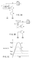
- FIG. 3A shows the construction of a stacked MOSFET protection circuit according to a first embodiment of the present invention.
- the protection circuit which is intended to protect the internal circuit of the semiconductor device against an external surge entering from, for example, an external power source pad, comprises a pad 1 for supplying an external power source Vext, a stacked MOSFET structure consisting of first and second MOSFET's Q1 and Q2 connected in series, and a clamping circuit 3.
- the clamping circuit 3 which is a two terminal circuit having a first terminal connected a node A of the stacked MOSFET protection circuit and a second terminal connected to a node B shown in FIG. 3A, serves to maintain constant the voltage V AB between the first and second terminals A and B regardless of the current value. By connecting the clamping circuit 3, it is possible to prevent the gate-drain voltage VGD of the MOSFET Q1 from exceeding the voltage BV GDm at which the gate insulating film incurs an unrecoverable breakdown at the drain edge.
- the protection circuit can be put in an "OFF" state during the normal operation of the semiconductor integrated circuit.
- the stacked MOSFET protection circuit is capable of providing a protection circuit exhibiting a value of the snap-back voltage VSB adapted for the reliability assurance of the semiconductor device without giving any detrimental effect to the normal operation.
- FIG. 3C a solid line in FIG. 3C denotes the surge absorption wave form in node B shown in FIGS. 3A and 3B.
- a thick broken line in FIG. 3C denotes the surge absorption wave form in node A shown in FIGS. 3A and 3B.
- the difference between the snap-back voltage V SBB in node B and the snap-back voltage V SBA in node A and the difference between the voltage V DBB in node B and the voltage V DBA in node A when the MOSFET's Q1 and Q2 are turned on correspond to the terminal voltage V AB of the clamping circuit 4 shown in FIG. 3A or the clamp voltage nV F of the clamp diode D i connected in series as shown in FIG. 3B.
- the stacked MOSFET protection circuit of the second embodiment is a circuit performing the function of an input and output buffer connected to an I/O pad of the semiconductor device and also performs the function of protecting the internal circuit of the semiconductor device from the external surge entering through the I/O pad.
- the stacked MOSFET protection circuit shown in FIG. 4A comprises a stacked MOSFET structure consisting of the first and second MOSFET's Q1 and Q2 connected in series, an I/O pad 4, and a switching circuit 5.
- the stacked MOSFET's Q1 and Q2 constitutes an output buffer circuit connected to the I/O pad 4.
- the switching circuit 5 including a resistor circuit for determining the output impedance of the buffer circuit and a supply terminal of the internal power source Vint serving to impart a gate bias is connected between the gate and the drain of the MOSFET Q1.
- the switching circuit 5 is a 3-terminal circuit having first, second and third terminals.
- the first and second terminals of the switching circuit 5 are connected to nodes A and B, respectively, of the stacked MOSFET protection circuit, and the third terminal of the switching circuit 5 is connected to the supply terminal of the internal power source Vint.
- a switching element is connected between the first and second terminals.
- the switching circuit 5 will now be described. Where the stacked MOSFET's Q1 and Q2 perform the normal operation as an output buffer connected to the I/O pad 4, the switching element is in an "OFF" state, and the gate bias voltage VG of the MOSFET Q1 required for operating the output buffer circuit is supplied from the first terminal connected to node A. It should be noted that the gate bias voltage VG is a voltage of the internal power source voltage Vint supplied to the third terminal and outputted from the first terminal via the switching circuit 5 including the resistor circuit.
- the switching element is turned “ON".
- the switching circuit 5 is operated to permit the difference V AB constant between the voltage of the second terminal connected to node B and the voltage of the first terminal connected to node A regardless of the current value flowing from the second terminal that is under the "ON" state.
- the switching circuit 5 performing the particular function is connected, it is possible to prevent the gate-source voltage VGD of the MOSFET Q1, which is equal to V AB , from exceeding the voltage BV GDm at which an unrecoverable breakdown of the gate insulating film occurs at the drain edge.
- the switching circuit 5 is detached from the drain (node B) of the MOSFET Q1, and the bias voltage VG during the normal operation is supplied from the internal power source Vint to the gate (node A) of the MOSFET Q1 through the switching circuit 5.
- the stacked MOSFET protection circuit of the second embodiment performs the function of an output buffer connected to the I/O pad and also performs the function of protecting the internal circuit of the semiconductor device from the external surge entering through the I/O pad.
- a stacked MOSFET protection circuit in which the switching circuit 5 is formed of diodes and a resistor will now be described as a first example of the second embodiment of the present invention.
- FIG. 4B shows a stacked MOSFET protection circuit in which a switching circuit 5a denoted by a broken line is formed of diodes and a resistor.
- the protection circuit comprises an I/O pad 4 of a semiconductor device, a stacked MOSFET structure consisting of the first and second MOSFET's Q1 and Q2 connected in series, an internal power source terminal for supplying the internal power source Vint of the semiconductor device, an i-number of diodes D i , i being 1 to n, and n being a natural number, and a resistor R.
- a power source voltage Vext is supplied from the outside to the I/O pad 4.
- n of the diodes D i is obtained from the external power source voltage Vext and the internal power source voltage Vint of the semiconductor device by formula (1) given below: n > (Vext - Vint)/V F where V F represents the forward voltage of the diode.
- the number n of diodes is determined to meet formula (1) given above, it is possible to prevent the current of the external power source from flowing into the diodes D i connected in series, even if the external power source voltage Vext is applied to node B and the internal power source voltage Vint, which is lower than the external power source voltage Vext, is applied to node A during normal operation of the semiconductor device. It follows that, if Vext - Vint is, for example, about 0.5V, it suffices to connect a single diode. Also, if the difference between Vext and Vint is not lower than 1V, it is necessary to connect at least two diodes.
- the potential difference V AB between node B and node A is kept constant at nV F , and it is possible to prevent the breakdown of the gate insulating film at the drain edge portion of the MOSFET Q1 because the impedance of the diodes Di is much lower than that of the resistor R.
- the gate-drain voltage VGD of the MOSFET Q1 is lower than nV F as apparent from formula (1) given above.
- the series-connected circuit of the diodes D i connected to node B is cut-off as an "OFF" state.
- the resistor R serves to protect the internal circuit of the semiconductor device when a high surge voltage V is applied to the external power source pad 4 to permit a large current to flow through the diodes D i into the internal power source terminal.
- a stacked MOSFET protection circuit in which the switching circuit 5 is formed of a MOSFET and a resistor, will now be described as a second specific example of the second embodiment of the present invention.
- FIG. 4C shows the second specific example of the second embodiment of the present invention, in which a switching circuit 5b surrounded by a broken line consists of a P-channel MOSFET and a resistor R.
- the protection circuit shown in FIG. 4C comprises and I/O pad 4 of a semiconductor device, a stacked MOSFET structure consisting of the first and second MOSFET's Q1 and Q2 connected in series, an internal power source terminal for supplying the internal power source Vint of the semiconductor device, a P-channel MOSFET Q3 performing a switching function, and a resistor R.
- the external power source Vext is supplied to the I/O pad 4.
- the threshold voltage Vth of the P-channel MOSFET Q3 performing a switching function is obtained from the external power source voltage Vext and the internal power source voltage Vint by formula (2) given below: Vth > Vext - Vint
- the threshold voltage Vth of the P-channel MOSFET Q3 performing a switching function is determined to meet formula (2) given above, it is possible to prevent the current of the external power source from flowing into the P-channel MOSFET Q3 because the P-channel MOSFET Q3 is in an "OFF" state even if the external power source voltage Vext is applied to node B and the internal power source voltage Vint lower than Vext is applied to node A during normal operation of the semiconductor device.
- V AB (Vext - Vint)*R ON /(R ON + R) where R ON (R ON ⁇ R) represents the "ON" resistance of the P-channel MOSFET Q3.
- the surge voltage Vext is divided into the terminal voltages of R ON and R.
- the P-channel MOSFET Q3 connected to node B is cut-off as an "OFF" state, as denoted by formula (2).
- the resistor R serves to protect the internal circuit when a high surge voltage is applied to the external power source pad 1 to permit a large current to flow into the internal power source terminal through the P-channel MOSFET Q3.
- the surge absorption wave form of the stacked MOSFET protection circuit shown in FIGS. 4A, 4B and 4C is equal to the surge absorption wave form shown in FIG. 3C.
- the potential of node A follows the potential of node B even if a high surge voltage is applied to the I/O pad 4.
- the potential difference V AB between node B and node A is kept constant, making it possible to prevent the breakdown of the gate insulating film of the MOSFET Q1.
- FIG. 5A is a cross sectional view showing the construction of a region in which a clamp diode and a resistor R are formed, with FIG. 5B showing the pattern of the region.
- FIG. 5A is a cross sectional view along the line A-A shown in FIG. 5B. This example covers the case where a single PN junction diode is formed in an N-well.
- an N-well 12 forming a main body of the resistor R is formed in a P-type silicon substrate 11, and a P-type diffusion layer 13 is formed at one end portion of the N-well 12 so as to form a diode consisting of a PN junction, which is connected to one electrode of the resistor R.
- an N-type diffusion layer 14 is formed in a manner to surround the diode. The N-type diffusion layer 14 provides one ohmic contact for connecting the resistor R to the cathode of the diode and serves to permit the resistance value of the resistor R to be close to the design value with a high accuracy.
- N-type diffusion layer 15 is formed within the N-well 12 so as to provide the other ohmic contact of the resistor R.
- a P-type diffusion layer (guard ring) 16 for the channel cut is formed in a manner to surround the N-well 12 so as to improve the isolation properties of PN junction between the N-well 12 to which a high surge voltage is applied and the P-type silicon substrate.
- the P-type diffusion layer 16 serves to cut off an N-type inversion layer that is likely to expand on the upper surface of the P-type silicon substrate so as to improve the isolation properties of the N-well 12 under a high voltage.
- Reference numeral 17 shown in the drawings denotes an electrode of the guard ring mounted to the P-type diffusion layer 16.
- a reference numeral 18 denotes an electrode of node B shown in FIG. 4B.
- a reference numeral 19 denotes an electrode of node A.
- a reference numeral 20 denotes an electrode connected to the internal power source Vint.
- FIG. 5B shows the plan view of these structures.
- a reference numeral 11a denotes an insulating film covering the surface of the silicon substrate 11.
- FIG. 6 shows a specific example of applying a stacked MOSFET protection circuit according to a fourth embodiment of the present invention to an input/output portion of a semiconductor device.
- the fourth embodiment is directed to various combinations of the stacked MOSFET protection circuits of the present invention which are connected between the I/O pad of the semiconductor device and the internal circuit.
- the input circuit denoted by a solid line and surrounded by a broken line 21 in FIG. 6 is a surge protection circuit provided with a clamp diode D described previously in conjunction with FIG. 3B.
- the output circuit surrounded by a broken line 22 is a protection circuit provided with an output buffer function consisting of MOSFET's Q1', Q2', a diode D' and a resistor R'.
- a reference numeral 6a denotes an front stage output buffer.
- an I/O pad is connected to a connection terminal 8 via an operational amplifier 6.
- a protective resistor R'' is connected to one input terminal of the operational amplifier 6 in order to protect the operational amplifier 6 from the surge entrance from the I/O pad, and a reference voltage Vref is applied to the other input terminal.
- the resistor R is connected to the internal power source terminal Vint as denoted by a broken line within the input circuit 21, it is possible to use the input circuit 21 as an input buffer provided with a surge protecting function. It is also possible to use commonly the resistors R, R' and the internal power source terminal Vint in the input circuit 21 functioning as an input buffer and in the output circuit 22 functioning as an output buffer so as to provide the function as an input-output buffer connected to the I/O pad and the surge protecting function against ESD or the like entering through the I/O pad.
- a single diode D is included in the input circuit 21 and a single diode D' is included in the output circuit 22 in the example shown in FIG. 6. Needless to say, however, it is possible for the input circuit 21 and the output circuit 22 to include a plurality of diodes D and diodes D', respectively.
- the MOSFET's Q1 and Q2 are divided into a large number of MOSFET's arranged in parallel and each having a gate width of about 10 micrometers.
- the surge current entering node A from the I/O pad through the diode D flows uniformly in a divided fashion through the MOSFET Q1 consisting of a large number of MOSFET's each having a small gate width, making it possible to improve the tolerance to surge of the MOSFET Q1 itself.
- the node N between the MOSFET's Q1 and Q2 are connected to each other to form a common node.
- a complementary stacked MOSFET protection circuit according to a fifth embodiment of the present invention will now be described with reference to FIG. 8. If the surge protection circuit of the present invention is applied to, for example, a CMOS type semiconductor device formed by using an internal power source Vint and the ground potential GND, it basically suffices to connect the surge protection circuit on the side of the N-channel MOSFET described in conjunction with the first to fourth embodiments to the surge protection circuit on the side of the inverted P-channel MOSFET by using a common drain.
- FIG. 8 shows the construction of a complementary stacked MOSFET protection circuit.
- the complementary stacked MOSFET protection circuit comprises N-channel MOSFET's Q1, Q2, P-channel MOSFET's Q3, Q4, diodes D1, D2, resistors R1, R2, and external power sources Vext, internal power sources Vint1 and Vint2.
- the gate biases of the MOSFET's Q1, Q3, are given by Vint1, Vint2, and the resistors R1, R2.
- the I/O buffer is formed in the same circuit configuration as the ESD protection circuit.
- protection circuit shown in FIG. 8 is used as a complementary output buffer
- complementary signals are supplied through lines 24, 25 to the gates of the MOSFET's Q2, Q4, respectively, and signals are outputted through the I/O pad connected to the common drain of the MOSFET's Q1, Q2.
- the protection circuit shown in FIG. 8 will now be described. If a positive surge voltage is applied to the I/O pad in the complementary stacked MOSFET protection circuit comprising a single or a plurality of diodes D1, D2, the surge voltage is absorbed by the snap-back characteristics of the N-channel MOSFET's Q1, Q2, and the diodes D1 serves to prevent the breakdown of the gate insulating film in drain edge portion of the MOSFET Q1.
- the surge voltage is absorbed by the snap-back characteristics of the P-channel MOSFET'S Q3, Q4, and the diode D2 serves to prevent breakdown of the gate insulating film in the drain edge portion of the MOSFET Q3.
- n1 (Vext - Vint1)/V F
- N2 (Vint2 - 0)/V F .
- the diodes D1 and D2 are cut off from the gates of the MOSFET's Q1, Q3, and a bias voltage required for operation as an output buffer is supplied from Vint1, Vint2 to the gates of the MOSFET's Q1, Q3.
- the complementary stacked MOSFET protection circuit shown in FIG. 8 exhibits the TDDB and HCI reliability and ESD endurance of the complementary semiconductor device without giving any detrimental effect to the normal operation as an output buffer.
- the resistors R1, R2 serve to stabilize the clamping characteristics of diodes D1, D2, and to protect the diodes D1, D2 and the internal circuit when a high surge voltage is applied to the I/O pad to permit a large current to flow into the internal power source terminals Vint1, Vint2 through the diodes D1 and D2.
- the present invention is not limited to the embodiments described above.
- a resistor circuit consisting of a plurality of resistors or an impedance element in place of the protective resistor R.
- a switching element consisting of, for example, a MOSFET in place of the diode, as already described in conjunction with the second embodiment.
- application of the first to fifth embodiments is not limited to an external power source pad or an I/O pad. These embodiments can be applied to the general portions where an external surge may possibly enter. Further, the present invention can be applied in various modified fashions within the technical scope of the present invention.
- a diode or a MOSFET is connected between the gate and the drain of the first MOSFET, where breakdown of the gate insulating film tends to take place in the conventional circuit.
- the protection circuit of the particular construction exhibits a snap-back voltage appropriate for assuring the reliability of the semiconductor integrated circuit and makes it possible to avoid breakdown of the gate insulating film.
- the current of the protection circuit is cut off and a voltage higher than a predetermined level is not applied across the gate insulating film during normal operation of the semiconductor integrated circuit. It follows that problems in terms of the reliability such as HCI and TDDB do not take place.
Landscapes
- Engineering & Computer Science (AREA)
- Power Engineering (AREA)
- Metal-Oxide And Bipolar Metal-Oxide Semiconductor Integrated Circuits (AREA)
- Semiconductor Integrated Circuits (AREA)
- Electronic Switches (AREA)
Abstract
Description
- The present invention relates to protection for ESD (Electro Static Discharge) of a semiconductor device, particularly, to a protection circuit against an ESD surge and an external excess voltage using a stacked MOSFET structure.
- In the conventional protection circuit of a semiconductor device, a discharging circuit consisting of combination of a diode and a resistor is formed between the input pad and the ground or between the output pad and the ground so as to discharge the static charge accumulated in the pins of the package in the assembling and mounting procedure so as to prevent the electrostatic breakdown.
- On the other hand, the scaling is a very effective means for the high integration degree and the high operating speed of an LSI. In accordance with the scaling of the process, the operation voltage is also subjected to the scaling in view of the voltage tolerance.
- However, the I/O interface voltage is slow in the progress of the scaling of the power source voltage, compared with the device, with the result that it is highly required that the low operating voltage and the high I/O interface voltage be satisfied simultaneously. An I/O formation technology tolerant to other power sources is known to the art as a technology that satisfies this requirement without giving rise to a process overhead.
- In general, in the case of using an output buffer, the external voltage is higher than the internal operation voltage so as to give rise to a problem in respect of the reliability of the gate insulating film. In other words, a reliability problem represented by TDDB (Time-Dependent Dielectric Breakdown) and HCI (Hot Carrier Injection) tends to be generated.
- In order to overcome the problem noted above, it was customary in the past to use a protection technology utilizing a stacked structure of MOSFFT's, as shown in FIG. 1A. For the sake of simplicity, N-channel MOSFET's alone are stacked in the circuit shown in FIG. 1A. As shown in the drawing, N-channel MOSFET's Q1 and Q2 are connected in series between a
pad 1 of an external power source Vext and the ground (GND) so as to form a stacked structure of MOSFET's. An internal power source Vint is applied to aninternal voltage terminal 2 connected to the gate of the MOSFET Q1. Incidentally, voltage of 0V to Vint is applied to theterminal 2a connected to the gate of the MOSFET Q2. - In the case of using the stacked structure of MOSFET's shown in FIG. 1A, the gate-drain voltage VGD of the MOSFET and the gate-source voltage VGS of the MOSFET is lower than Vint, i.e., VGD, VGS < Vint, so as to assure the TDDB reliability. Further, since the drain-source voltage VDS divides Vext, the HCI reliability is also ensured.
- Concerning the MOSFET Q2, the drain voltage is held at Vint - Vth, where Vth represents the threshold voltage, so as to avoid the problem in terms of the reliability.
- In recent years, in a semiconductor device using a different power source technology provided with the external power source Vext and the internal power source Vint, a protection circuit of I/O's tolerant to other power sources having a stacked structure of MOSFET's in which the MOSFET's Q1 and Q2 are connected in series between the
pad 1 and GND is used as a protection circuit exhibiting a high surge tolerance against the surge entering through, for example, thepad 1, as shown in FIGS. 1A and 1B. - FIG. 1B shows the equivalent circuit of FIG. 1A and the problem in the case where a surge voltage V is applied to the
pad 1 for a short time. The external surge voltage V enters thepad 1 for various reasons. For example, the external surge voltage is generated in the case of ESD in which the charge added to the surrounding portions in the assembling, testing and mounting steps to a system is discharged through the pins of the package. - In the structure shown in FIGS. 1A and 1B, it is possible for the breakdown of the protection circuit to take place in the case where the surge voltage V is applied for a short time to the
pad 1. To be more specific, under the state that, although the gate of the MOSFET Q1 is connected to Vint, the power source is not turned on as shown in FIG. 1A, the gate of the MOSFET Q1 bears the ground potential. In addition, since a very large equivalent capacitance is connected to Vint, the gate-drain voltage VGD of the MOSFET Q1 exceeds the withstand voltage of the gate insulating film during application of the surge voltage V. As a result, the MOSFET Q1 is broken down before the snap-back characteristics of the MOSFET effective for the surge absorption perform their functions. - The breakdown process of the MOSFET Q1 during application of the surge voltage V to the
pad 1 will now be described with reference to the equivalent circuit shown in FIG. 1B. If the surge voltage V is applied to the equivalent circuit shown in FIG. 1B, the electron-hole avalanche takes place on the channel surface on the drain side of the MOSFET Q1. As a result, a large current flows between the source and drain of the MOSFET Q1, and the surge voltage applied to the externalpower source pad 1 is rapidly lowered by the discharge current. It follows that the stacked MOSFET protection circuit exhibits excellent snap-back characteristics. - However, since a high surge voltage V is applied to the stacked MOSFET protection circuit consisting of the MOSFET's Q1 and Q2, the greatest gate-drain voltage VGD is applied to the drain edge portion of the gate insulating film of the MOSFET Q1 as denoted by a circle 10 of a broken line in FIG. 1B, giving rise to the problem that the gate insulating film is broken down at the portion denoted by the broken circle 10.
- On the other hand, it was attempted to use a protection circuit of one stage MOSFET in which the drain of the MOSFET Q2 is connected directly to the
pad 1. In the protection circuit of one stage MOSFET, the drain voltage of the MOSFET Q2 is lowered by an amount equal to the source-drain voltage of the MOSFET Q1 so as to lower the maximum gate-drain voltage VGD applied to the drain edge of the gate insulating film of the MOSFET Q2 so as to suppress the breakdown of the gate insulating film. - FIG. 2 compares the snap-back characteristics of the stacked MOSFET protection circuit consisting of the MOSFET's Q1 and Q2 with those of protection circuit of the one stage MOSFET consisting of the MOSFET Q2 alone.
- In FIG. 2, the snap-back voltage of the stacked structure is denoted by VSB' which is denoted by a thick broken line, the drain voltage in the "ON" state is denoted by VDB. The phenomenon called in general a second breakdown causes the snap-back curves in the transition region in which VSB is switched to VDB to show two steps.
- On the other hand, the snap-back voltage VSB' and the drain voltage VDB' under the "ON" state for the one stage MOSFET, which are denoted by a thin solid curve, are lower than the snap-back voltage VSD and the drain voltage VDB under the "ON" state, respectively, for the stacked MOSFET structure, which are denoted by a thick broken curve.
- If the surge voltage V caused by, for example, ESD is applied to the
pad 1, the protection circuit is repeatedly switched along the curves of the snap-back characteristics shown in FIG. 2, with the result that the protection circuit is capable of performing the surge protection of the semiconductor integrated circuit until the breakdown 10 of the gate insulating film shown in FIG. 1B is made unrecoverable. - As described previously, the snap-back voltage VSB' of the conventional one stage MOSFET protection circuit is lower than the snap-back voltage VSB of the protection circuit of the stacked structure so as to produce a merit that the occurrence of the breakdown 10 of the gate insulating film can be suppressed. On the other hand, the conventional one stage MOSFET protection circuit is defective in that it is impossible to set the snap-back voltage VSB' at a sufficiently large value relative to the maximum rating of the external power source voltage required for the reliability assurance of the semiconductor device.
- As described above, where a stacked structure of MOSFET's is used as a protection circuit against ESD, serious problems are left unsolved. In general, similar problems are generated in the case of using a stacked MOSFET protection circuit against the external surge voltage.
- As described above, the conventional stacked MOSFET protection circuit is defective in that the gate insulating film of the first MOSFET tends to be broken down at the edge of the drain. Also, the conventional one stage MOSFET protection circuit is defective in that it is incapable of sufficiently assuring the TDDB and HCI reliability of the semiconductor device.
- An object of the present invention, which has been achieved in an attempt to overcome the above-noted problems inherent in the prior art, is to provide a stacked MOSFET protection circuit capable of sufficiently assuring the TDDB and HCI reliability of the semiconductor device and capable of avoiding the breakdown of the gate insulating film.
- In the protection circuit of the present invention, a clamping circuit consisting of, for example, a clamp diode is connected between the gate and the source of a MOSFET constituting the stacked MOSFET circuit so as to release an excess voltage and, thus, to avoid the breakdown of the gate insulating film caused by application of the excess voltage between the gate and the drain of the MOSFET. The stacked MOSFET protection circuit provided with such a clamping circuit is adapted for a protection circuit against an external surge entering from, particularly, the external power source pad.
- The protection circuit of the present invention is also featured in that, in order to avoid the breakdown, caused by the excess voltage, of the gate insulating film of the MOSFET constituting the stacked protection circuit, the circuit is provided with a switching circuit consisting of a diode that is turned on when the excess voltage is applied between the gate and the drain of the MOSFET and a resistor or consisting of a MOSFET and a resistor. The stacked protection circuit of the MOSFET provided with the particular switching circuit is adapted for use as, particularly, a protection circuit of an input/output buffer consisting of MOSFET's connected to an I/O pad.
- According to a first aspect of the present invention, there is provided a protection circuit, comprising first and second MOS transistors having the source of the first MOS transistor connected to the drain of the second MOS transistor; a clamping circuit having first and second terminals, the first terminal being connected to the gate of the first MOS transistor and the second terminal being connected to the drain of the first MOS transistor; and a pad connected to the drain of the first MOS transistor.
- It is desirable for the clamping circuit to serve to maintain constant the potential difference between the first and second terminals when the surge voltage enters the pad.
- It is desirable for the source and gate of the second MOS transistor to be connected to the ground.
- It is desirable for the clamping circuit to consist of a diode. In this case, the cathode of the diode forms the first terminal of the clamping circuit with the anode of the diode forming the second terminal of the clamping circuit.
- It is also desirable for the clamping circuit to consist of a plurality of diodes having the cathode of each diode connected to the anode of the adjacent diode, wherein the cathode forming end portion on one side of the plural diodes constitute the first terminal of the clamping circuit, and the anode forming end portion on the other side of the plural diodes constitute the second terminal of the clamping circuit.
- According to a second aspect of the present invention, there is provided a protection circuit, comprising first and second MOS transistors having the source of the first MOS transistor connected to the drain of the second MOS transistor; a switching circuit having first, second and third terminals, the first terminal being connected to the gate of the first MOS transistor, the second terminal being connected to the drain of the first MOS transistor, and the third terminal being connected to the internal power source of the semiconductor device, and a pad connected to the drain of the first MOS transistor.
- It is desirable for the switching circuit to serve to electrically cut-off the second terminal during the normal operation of the semiconductor device and to maintain constant the potential difference between the first and second terminals when the surge voltage enters the pad.
- It is desirable for the switching circuit to consist of a diode. In this case, the cathode of the diode is connected to the gate of the first MOS transistor so as to form the first terminal of the switching circuit, and the anode of the diode forms the second terminal of the switching circuit. Further, the cathode of the diode is connected to the internal power source of the semiconductor device so as to form the third terminal of the switching circuit. More preferably, the cathode of the diode is connected via a resistor circuit to the internal power source of the semiconductor device so as to form the third terminal of the switching circuit.
- It is desirable for the switching circuit to consist of a plurality of diodes having the cathode of each diode connected to the anode of the adjacent diode. In this case, the cathode forming end portion on one side of the diodes are connected to the gate of the first MOS transistor so as to form the first terminal of the switching circuit, and the anode forming end portion on the other side of the diodes form the second terminal of the switching circuit. Further, the cathode forming end portion on one side of the diodes are connected to the internal power source of the semiconductor device so as to form the third terminal of the switching circuit. More preferably, the cathode forming end portion on one side of the diodes are connected via a resistor circuit to the internal power source of the semiconductor device so as to form the third terminal of the switching circuit.
- More preferably, the number n (n being a natural number) of the plural diodes is selected to meet the relationship
- More preferably, the switching circuit consists of a third MOS transistor with an inverse conductivity type of the first and second MOS transistors, wherein the source of the third MOS transistor is connected to the gate of the first MOS transistor so as to form the first terminal of the switching circuit, the drain of the third MOS transistor forms the second terminal of the switching circuit, the source of the third MOS transistor is connected to the gate of the third MOS transistor, and the gate of the third MOS transistor is connected via a resistor to the internal power source of the semiconductor device so as to form the third terminal.
- More preferably, the threshold voltage Vth of the third MOS transistor is selected to meet the relationship
- Further, according to a third aspect of the present invention, there is provided a protection circuit, comprising first and second MOS transistors of a first conductivity type, third and fourth MOS transistors of a second conductivity type, first and second diodes, first and second resistors, an input/output pad, and first, second and third power sources, wherein:
- the source of the first MOS transistor is connected to the drain of the second MOS transistor, the source of the third MOS transistor is connected to the drain of the fourth MOS transistor, and each of the drain of the first MOS transistor and the drain of the third MOS transistor is connected to the input/output pad;
- the cathode of the first diode is connected to the gate of the first MOS transistor and to the first power source via the first resistor, the anode of the first diode is connected to the input/output pad, the anode of the second diode is connected to the gate of the third MOS transistor and to the second power source via the second resistor, and the cathode of the second diode is connected to the input/output pad; and
- the source of the fourth MOS transistor is connected to the third power source, and the source of the second MOS transistor is connected to the ground.
-
- This summary of the invention does not necessarily describe all necessary features so that the invention may also be a sub-combination of these described features.
- The invention can be more fully under stood from the following detailed description when taken in conjunction with the accompanying drawings, in which:
- FIG. 1A shows the circuit construction of a conventional stacked MOSFET protection circuit in the normal operation;
- FIG. 1B shows the equivalent circuit of the conventional stacked MOSFET protection circuit during surge voltage application;
- FIG. 2 compares the snap-back characteristics of the stacked MOSFET structure with those of a single stage MOSFET protection circuit;
- FIG. 3A shows the construction of a stacked MOSFET protection circuit according to a first embodiment of the present invention;
- FIG. 3B shows the construction of a stacked MOSFET protection circuit using diodes according to the first embodiment of the present invention;
- FIG. 3C shows the surge absorption wave form of the stacked MOSFET protection circuit according to the first embodiment of the present invention;
- FIG. 4A shows the stacked MOSFET protection circuit according to a second embodiment of the present invention;
- FIG. 4B shows the construction of a stacked MOSFET protection circuit using diodes and a resistor according to the second embodiment of the present invention;
- FIG. 4C shows the construction of a stacked MOSFET protection circuit using a MOSFET and a resistor according to the second embodiment of the present invention;
- FIG. 5A is a cross sectional view showing the construction of switching (clamping) elements of a stacked MOSFET protection circuit according to a third embodiment of the present invention;
- FIG. 5B shows a plan view of switching (clamping) elements of the stacked MOSFET protection circuit according to the third embodiment of the present invention;
- FIG. 6 shows various applications of a stacked MOSFET protection circuit according to a fourth embodiment of the present invention;
- FIG. 7 shows the construction of the MOSFET's Q1, Q2 according to the fourth embodiment of the present invention; and
- FIG. 8 shows the construction of a complementary stacked MOSFET protection circuit according to a fifth embodiment of the present invention.
-
- Some embodiments of the present invention will now be described in detail with reference to the accompanying drawings.
- FIG. 3A shows the construction of a stacked MOSFET protection circuit according to a first embodiment of the present invention. The protection circuit, which is intended to protect the internal circuit of the semiconductor device against an external surge entering from, for example, an external power source pad, comprises a
pad 1 for supplying an external power source Vext, a stacked MOSFET structure consisting of first and second MOSFET's Q1 and Q2 connected in series, and aclamping circuit 3. - The
clamping circuit 3, which is a two terminal circuit having a first terminal connected a node A of the stacked MOSFET protection circuit and a second terminal connected to a node B shown in FIG. 3A, serves to maintain constant the voltage VAB between the first and second terminals A and B regardless of the current value. By connecting theclamping circuit 3, it is possible to prevent the gate-drain voltage VGD of the MOSFET Q1 from exceeding the voltage BVGDm at which the gate insulating film incurs an unrecoverable breakdown at the drain edge. - To be more specific, the
clamping circuit 3 can be formed by using a forward voltage VF of a diode. If a plurality of diodes Di (i = 1 to n, n being a natural number) are connected in series as denoted by broken line 3a in FIG. 3B, VAB is equal to nVF, ( - Incidentally, if the MOSFET Q2 is of a normally-off type, the protection circuit can be put in an "OFF" state during the normal operation of the semiconductor integrated circuit. Thus, the stacked MOSFET protection circuit is capable of providing a protection circuit exhibiting a value of the snap-back voltage VSB adapted for the reliability assurance of the semiconductor device without giving any detrimental effect to the normal operation.
- The operation of the stacked MOSFET protection circuit will now be described more in detail with reference to FIG. 3C. Specifically, a solid line in FIG. 3C denotes the surge absorption wave form in node B shown in FIGS. 3A and 3B. On the other hand, a thick broken line in FIG. 3C denotes the surge absorption wave form in node A shown in FIGS. 3A and 3B.
- As shown in FIG. 3C, the difference between the snap-back voltage VSBB in node B and the snap-back voltage VSBA in node A and the difference between the voltage VDBB in node B and the voltage VDBA in node A when the MOSFET's Q1 and Q2 are turned on correspond to the terminal voltage VAB of the
clamping circuit 4 shown in FIG. 3A or the clamp voltage nVF of the clamp diode Di connected in series as shown in FIG. 3B. As described above, even if a high surge voltage VSBB is applied to thepad 1, the voltage at node A is clamped at the level shifted voltage shifted by VAB or nVF from the voltage at node B, making it possible to prevent the breakdown of the gate insulating film of the MOSFET Q1. - A stacked MOSFET protection circuit according to a second embodiment of the present invention will now be described with reference to FIG. 4A. The stacked MOSFET protection circuit of the second embodiment is a circuit performing the function of an input and output buffer connected to an I/O pad of the semiconductor device and also performs the function of protecting the internal circuit of the semiconductor device from the external surge entering through the I/O pad.
- The stacked MOSFET protection circuit shown in FIG. 4A comprises a stacked MOSFET structure consisting of the first and second MOSFET's Q1 and Q2 connected in series, an I/
O pad 4, and a switching circuit 5. The stacked MOSFET's Q1 and Q2 constitutes an output buffer circuit connected to the I/O pad 4. As shown in the drawing, the switching circuit 5 including a resistor circuit for determining the output impedance of the buffer circuit and a supply terminal of the internal power source Vint serving to impart a gate bias is connected between the gate and the drain of the MOSFET Q1. - The switching circuit 5 is a 3-terminal circuit having first, second and third terminals. The first and second terminals of the switching circuit 5 are connected to nodes A and B, respectively, of the stacked MOSFET protection circuit, and the third terminal of the switching circuit 5 is connected to the supply terminal of the internal power source Vint.
- A switching element is connected between the first and second terminals.
- The operation of the switching circuit 5 will now be described. Where the stacked MOSFET's Q1 and Q2 perform the normal operation as an output buffer connected to the I/
O pad 4, the switching element is in an "OFF" state, and the gate bias voltage VG of the MOSFET Q1 required for operating the output buffer circuit is supplied from the first terminal connected to node A. It should be noted that the gate bias voltage VG is a voltage of the internal power source voltage Vint supplied to the third terminal and outputted from the first terminal via the switching circuit 5 including the resistor circuit. - Where the stacked MOSFET's Q1 and Q2 absorb the external surge voltage entering through the I/
O pad 4, the switching element is turned "ON". The switching circuit 5 is operated to permit the difference VAB constant between the voltage of the second terminal connected to node B and the voltage of the first terminal connected to node A regardless of the current value flowing from the second terminal that is under the "ON" state. - If the switching circuit 5 performing the particular function is connected, it is possible to prevent the gate-source voltage VGD of the MOSFET Q1, which is equal to VAB, from exceeding the voltage BVGDm at which an unrecoverable breakdown of the gate insulating film occurs at the drain edge.
- Also, during the normal operation, the switching circuit 5 is detached from the drain (node B) of the MOSFET Q1, and the bias voltage VG during the normal operation is supplied from the internal power source Vint to the gate (node A) of the MOSFET Q1 through the switching circuit 5. As a result, the stacked MOSFET protection circuit of the second embodiment performs the function of an output buffer connected to the I/O pad and also performs the function of protecting the internal circuit of the semiconductor device from the external surge entering through the I/O pad.
- A stacked MOSFET protection circuit in which the switching circuit 5 is formed of diodes and a resistor will now be described as a first example of the second embodiment of the present invention.
- FIG. 4B shows a stacked MOSFET protection circuit in which a
switching circuit 5a denoted by a broken line is formed of diodes and a resistor. The protection circuit comprises an I/O pad 4 of a semiconductor device, a stacked MOSFET structure consisting of the first and second MOSFET's Q1 and Q2 connected in series, an internal power source terminal for supplying the internal power source Vint of the semiconductor device, an i-number of diodes Di, i being 1 to n, and n being a natural number, and a resistor R. A power source voltage Vext is supplied from the outside to the I/O pad 4. - The number n of the diodes Di is obtained from the external power source voltage Vext and the internal power source voltage Vint of the semiconductor device by formula (1) given below:
- If the number n of diodes is determined to meet formula (1) given above, it is possible to prevent the current of the external power source from flowing into the diodes Di connected in series, even if the external power source voltage Vext is applied to node B and the internal power source voltage Vint, which is lower than the external power source voltage Vext, is applied to node A during normal operation of the semiconductor device. It follows that, if Vext - Vint is, for example, about 0.5V, it suffices to connect a single diode. Also, if the difference between Vext and Vint is not lower than 1V, it is necessary to connect at least two diodes.
- If a surge voltage V higher than the external power source voltage Vext is applied to the
pad 4 in the stacked MOSFET protection circuit provided with a single or a plurality of diodes Di, the potential difference VAB between node B and node A is kept constant at nVF, and it is possible to prevent the breakdown of the gate insulating film at the drain edge portion of the MOSFET Q1 because the impedance of the diodes Di is much lower than that of the resistor R. - During normal operation of the semiconductor device, the gate-drain voltage VGD of the MOSFET Q1 is lower than nVF as apparent from formula (1) given above. Thus, the series-connected circuit of the diodes Di connected to node B is cut-off as an "OFF" state. Also, the bias voltage VG required for operating the output buffer is supplied from Vint (VG = Vint in this case) to the gate of the MOSFET Q1 through the resistor R. It follows that the stacked MOSFET protection circuit exhibits a suitable snap-back voltage for assuring the reliability of the semiconductor device without giving any detrimental effect to the normal operation as an output buffer. Incidentally, the resistor R serves to protect the internal circuit of the semiconductor device when a high surge voltage V is applied to the external
power source pad 4 to permit a large current to flow through the diodes Di into the internal power source terminal. - A stacked MOSFET protection circuit, in which the switching circuit 5 is formed of a MOSFET and a resistor, will now be described as a second specific example of the second embodiment of the present invention.
- FIG. 4C shows the second specific example of the second embodiment of the present invention, in which a
switching circuit 5b surrounded by a broken line consists of a P-channel MOSFET and a resistor R. The protection circuit shown in FIG. 4C comprises and I/O pad 4 of a semiconductor device, a stacked MOSFET structure consisting of the first and second MOSFET's Q1 and Q2 connected in series, an internal power source terminal for supplying the internal power source Vint of the semiconductor device, a P-channel MOSFET Q3 performing a switching function, and a resistor R. The external power source Vext is supplied to the I/O pad 4. - The threshold voltage Vth of the P-channel MOSFET Q3 performing a switching function is obtained from the external power source voltage Vext and the internal power source voltage Vint by formula (2) given below:
- If the threshold voltage Vth of the P-channel MOSFET Q3 performing a switching function is determined to meet formula (2) given above, it is possible to prevent the current of the external power source from flowing into the P-channel MOSFET Q3 because the P-channel MOSFET Q3 is in an "OFF" state even if the external power source voltage Vext is applied to node B and the internal power source voltage Vint lower than Vext is applied to node A during normal operation of the semiconductor device.
- If a surge voltage V higher than the external power source voltage Vext is applied for a short time to the I/
O pad 4 of the stacked MOSFET protection circuit provided with the P-channel MOSFET Q3, the P-channel MOSFET Q3 is rendered "ON" as described previously in conjunction with FIG. 1B because the internal power source terminal Vint is connected to the ground via a large equivalent capacitance C. In this case, the potential difference VAB between anode B and anode A is given by formula (3): - By making RON equivalent to the impedance of the resistor R, the surge voltage Vext is divided into the terminal voltages of RON and R.
- Since the potential difference VAB between node B and node A is as given by formula (3) while a surge voltage is kept applied to the I/
O pad 4, it is possible to prevent the breakdown of the gate insulating film in the drain edge portion of the MOSFET Q1, if the potential difference VAB meets the relationship given in formula (4): - During normal operation of the semiconductor device, the P-channel MOSFET Q3 connected to node B is cut-off as an "OFF" state, as denoted by formula (2). Also, a bias voltage required for operation as an output buffer is supplied from the internal power source terminal Vint (VG = Vint in this case) to the gate of the MOSFET Q1 through the resistor R. It follows that the stacked MOSFET protection circuit shown in FIG. 4C exhibits ESD endurance for assuring the reliability of the semiconductor device without giving any detrimental effect to the normal operation as the output buffer.
- Incidentally, the resistor R serves to protect the internal circuit when a high surge voltage is applied to the external
power source pad 1 to permit a large current to flow into the internal power source terminal through the P-channel MOSFET Q3. The surge absorption wave form of the stacked MOSFET protection circuit shown in FIGS. 4A, 4B and 4C is equal to the surge absorption wave form shown in FIG. 3C. - As described above, the potential of node A follows the potential of node B even if a high surge voltage is applied to the I/
O pad 4. As a result, the potential difference VAB between node B and node A is kept constant, making it possible to prevent the breakdown of the gate insulating film of the MOSFET Q1. - The construction of a stacked MOSFET protection circuit according to a third embodiment of the present invention will now be described with reference to FIGS. 5A and 5B. Specifically, FIG. 5A is a cross sectional view showing the construction of a region in which a clamp diode and a resistor R are formed, with FIG. 5B showing the pattern of the region. Incidentally, FIG. 5A is a cross sectional view along the line A-A shown in FIG. 5B. This example covers the case where a single PN junction diode is formed in an N-well.
- As shown in FIG. 5A, an N-well 12 forming a main body of the resistor R is formed in a P-
type silicon substrate 11, and a P-type diffusion layer 13 is formed at one end portion of the N-well 12 so as to form a diode consisting of a PN junction, which is connected to one electrode of the resistor R. Incidentally, an N-type diffusion layer 14 is formed in a manner to surround the diode. The N-type diffusion layer 14 provides one ohmic contact for connecting the resistor R to the cathode of the diode and serves to permit the resistance value of the resistor R to be close to the design value with a high accuracy. - An N-
type diffusion layer 15 is formed within the N-well 12 so as to provide the other ohmic contact of the resistor R. Further, a P-type diffusion layer (guard ring) 16 for the channel cut is formed in a manner to surround the N-well 12 so as to improve the isolation properties of PN junction between the N-well 12 to which a high surge voltage is applied and the P-type silicon substrate. The P-type diffusion layer 16 serves to cut off an N-type inversion layer that is likely to expand on the upper surface of the P-type silicon substrate so as to improve the isolation properties of the N-well 12 under a high voltage. -
Reference numeral 17 shown in the drawings denotes an electrode of the guard ring mounted to the P-type diffusion layer 16. Areference numeral 18 denotes an electrode of node B shown in FIG. 4B. Areference numeral 19 denotes an electrode of node A. Further, areference numeral 20 denotes an electrode connected to the internal power source Vint. FIG. 5B shows the plan view of these structures. Incidentally, areference numeral 11a denotes an insulating film covering the surface of thesilicon substrate 11. - FIG. 6 shows a specific example of applying a stacked MOSFET protection circuit according to a fourth embodiment of the present invention to an input/output portion of a semiconductor device. The fourth embodiment is directed to various combinations of the stacked MOSFET protection circuits of the present invention which are connected between the I/O pad of the semiconductor device and the internal circuit.
- The input circuit denoted by a solid line and surrounded by a
broken line 21 in FIG. 6 is a surge protection circuit provided with a clamp diode D described previously in conjunction with FIG. 3B. On the other hand, the output circuit surrounded by abroken line 22 is a protection circuit provided with an output buffer function consisting of MOSFET's Q1', Q2', a diode D' and a resistor R'. Incidentally, a reference numeral 6a denotes an front stage output buffer. - In the internal circuit surrounded by the
broken line 23, an I/O pad is connected to aconnection terminal 8 via anoperational amplifier 6. A protective resistor R'' is connected to one input terminal of theoperational amplifier 6 in order to protect theoperational amplifier 6 from the surge entrance from the I/O pad, and a reference voltage Vref is applied to the other input terminal. - It is possible to achieve a satisfactory function of protecting the internal circuit against surge by combining a surge protection circuit against ESD or the like denoted by a solid line portion of the
input circuit 21 an internal circuit connected to, for example, theterminal 8. - In this case, if the resistor R is connected to the internal power source terminal Vint as denoted by a broken line within the
input circuit 21, it is possible to use theinput circuit 21 as an input buffer provided with a surge protecting function. It is also possible to use commonly the resistors R, R' and the internal power source terminal Vint in theinput circuit 21 functioning as an input buffer and in theoutput circuit 22 functioning as an output buffer so as to provide the function as an input-output buffer connected to the I/O pad and the surge protecting function against ESD or the like entering through the I/O pad. Incidentally, a single diode D is included in theinput circuit 21 and a single diode D' is included in theoutput circuit 22 in the example shown in FIG. 6. Needless to say, however, it is possible for theinput circuit 21 and theoutput circuit 22 to include a plurality of diodes D and diodes D', respectively. - Some problems remain unsolved in the construction of the MOSFET's Q1, Q2 included in the stacked MOSFET protection circuit. These problems will now be described with reference to FIG. 7. It is necessary for the MOSFET's Q1 and Q2 to absorb a large surge current and, thus, these MOSFET's are required to have several hundred micrometers of the gate width. If the gate width is increased, however, a partial gate breakdown is brought about, from nonuniformity of the device parameters caused by the parasitic resistance, etc., resulting in failure to obtain satisfactory surge protection characteristics.
- To avoid the difficulty noted above, the MOSFET's Q1 and Q2 are divided into a large number of MOSFET's arranged in parallel and each having a gate width of about 10 micrometers. In this case, the surge current entering node A from the I/O pad through the diode D flows uniformly in a divided fashion through the MOSFET Q1 consisting of a large number of MOSFET's each having a small gate width, making it possible to improve the tolerance to surge of the MOSFET Q1 itself. In this case, the node N between the MOSFET's Q1 and Q2 are connected to each other to form a common node.
- The construction of a complementary stacked MOSFET protection circuit according to a fifth embodiment of the present invention will now be described with reference to FIG. 8. If the surge protection circuit of the present invention is applied to, for example, a CMOS type semiconductor device formed by using an internal power source Vint and the ground potential GND, it basically suffices to connect the surge protection circuit on the side of the N-channel MOSFET described in conjunction with the first to fourth embodiments to the surge protection circuit on the side of the inverted P-channel MOSFET by using a common drain.
- FIG. 8 shows the construction of a complementary stacked MOSFET protection circuit. As shown in the drawing, the complementary stacked MOSFET protection circuit comprises N-channel MOSFET's Q1, Q2, P-channel MOSFET's Q3, Q4, diodes D1, D2, resistors R1, R2, and external power sources Vext, internal power sources Vint1 and Vint2.
- In the protection circuit shown in FIG. 8, the gate biases of the MOSFET's Q1, Q3, are given by Vint1, Vint2, and the resistors R1, R2. In this case, the I/O buffer is formed in the same circuit configuration as the ESD protection circuit. Alternatively, it suffices to use a circuit configuration of Q1, Q3 gates, which are not connected to Vint1 and Vint2, only for the purpose of ESD protection.
- Where the protection circuit shown in FIG. 8 is used as a complementary output buffer, complementary signals are supplied through
lines - The operation of the protection circuit shown in FIG. 8 will now be described. If a positive surge voltage is applied to the I/O pad in the complementary stacked MOSFET protection circuit comprising a single or a plurality of diodes D1, D2, the surge voltage is absorbed by the snap-back characteristics of the N-channel MOSFET's Q1, Q2, and the diodes D1 serves to prevent the breakdown of the gate insulating film in drain edge portion of the MOSFET Q1.
- If a negative surge voltage is applied to the I/O pad, the surge voltage is absorbed by the snap-back characteristics of the P-channel MOSFET'S Q3, Q4, and the diode D2 serves to prevent breakdown of the gate insulating film in the drain edge portion of the MOSFET Q3.
- If the diode D1 is formed of n1 diodes and the diode D2 is formed of n2 diodes, it is necessary to meet both conditions,
- During normal operation of the complementary semiconductor device, the diodes D1 and D2 are cut off from the gates of the MOSFET's Q1, Q3, and a bias voltage required for operation as an output buffer is supplied from Vint1, Vint2 to the gates of the MOSFET's Q1, Q3. As a result, the complementary stacked MOSFET protection circuit shown in FIG. 8 exhibits the TDDB and HCI reliability and ESD endurance of the complementary semiconductor device without giving any detrimental effect to the normal operation as an output buffer.
- Incidentally, the resistors R1, R2 serve to stabilize the clamping characteristics of diodes D1, D2, and to protect the diodes D1, D2 and the internal circuit when a high surge voltage is applied to the I/O pad to permit a large current to flow into the internal power source terminals Vint1, Vint2 through the diodes D1 and D2.
- The present invention is not limited to the embodiments described above. For example, in each of the first to fifth embodiments described above, it is possible to use a resistor circuit consisting of a plurality of resistors or an impedance element in place of the protective resistor R. Also, it is possible to use a switching element consisting of, for example, a MOSFET in place of the diode, as already described in conjunction with the second embodiment.
- As already described in conjunction with the fourth embodiment, application of the first to fifth embodiments is not limited to an external power source pad or an I/O pad. These embodiments can be applied to the general portions where an external surge may possibly enter. Further, the present invention can be applied in various modified fashions within the technical scope of the present invention.
- As described above, in the stacked MOSFET protection circuit of the present invention, a diode or a MOSFET is connected between the gate and the drain of the first MOSFET, where breakdown of the gate insulating film tends to take place in the conventional circuit. The protection circuit of the particular construction exhibits a snap-back voltage appropriate for assuring the reliability of the semiconductor integrated circuit and makes it possible to avoid breakdown of the gate insulating film.
- Also, according to the protection circuit of the present invention, the current of the protection circuit is cut off and a voltage higher than a predetermined level is not applied across the gate insulating film during normal operation of the semiconductor integrated circuit. It follows that problems in terms of the reliability such as HCI and TDDB do not take place.
Claims (17)
- A protection circuit, characterized by comprising:first and second MOS transistors having a source of the first MOS transistor connected to a drain of the second MOS transistor;a clamping circuit (3) having first and second terminals, said first terminal being connected to a gate of the first MOS transistor and said second terminal being connected to a drain of the first MOS transistor; anda pad (1) of a semiconductor device connected to the drain of the first MOS transistor.
- The protection circuit according to claim 1, characterized in that the clamping circuit (3) serves to maintain constant the potential difference between the first and second terminals when a surge voltage enters the pad (1).
- The protection circuit according to claim 1, characterized in that said clamping circuit (3a) consists of a diode, a cathode of said diode forming the first terminal of the clamping circuit (3a) with an anode of the diode forming the second terminal of the clamping circuit (3a).
- The protection circuit according to claim 1, characterized in that said clamping circuit (3a) consists of a plurality of diodes having a cathode of each diode connected to an anode of the adjacent diode, wherein a cathode forming end portion on one side of the plural diodes constitute the first terminal of the clamping circuit (3a), and an anode forming end portion on the other side of the plural diodes constitute the second terminal of the clamping circuit (3a).
- A protection circuit, characterized by comprising:first and second MOS transistors having a source of the first MOS transistor connected to a drain of the second MOS transistor;a switching circuit (5) having first, second and third terminals, said first terminal being connected to a gate of the first MOS transistor, said second terminal being connected to a drain of the first MOS transistor, and said third terminal being connected to an internal power source of a semiconductor device, anda pad (4) connected to the drain of the first MOS transistor.
- The protection circuit according to claim 5, characterized in that said switching circuit serves to electrically cut-off the second terminal during a normal operation of the semiconductor device and to maintain constant a potential difference between the first and second terminals when a surge voltage enters the pad (4).
- The protection circuit according to any one of claims 1 and 5, characterized in that the source and gate of the second MOS transistor are connected to the ground.
- The protection circuit according to any one of claims 1 and 5, characterized in that said pad (1) constitutes a power source pad of a semiconductor device.
- The protection circuit according to any one of claims 1 and 5, characterized in that said pad constitutes an input/output pad (1, 4) of a semiconductor device.
- The protection circuit according to claim 5, characterized in that said switching circuit (5a) consists of a diode, a cathode of said diode being connected to the gate of the first MOS transistor so as to form the first terminal of the switching circuit (5a), and an anode of said diode forming the second terminal of the switching circuit (5a), and the cathode of said diode being connected to the internal power source of the semiconductor device so as to form the third terminal of the switching circuit (5a).
- The protection circuit according to claim 10, characterized in that the cathode of the diode is connected via a resistor circuit to the internal power source of the semiconductor device so as to form the third terminal of the switching circuit (5a).
- The protection circuit according to claim 5, characterized in that said switching circuit (5a) consists of a plurality of diodes having a cathode of each diode connected to an anode of the adjacent diode, a cathode forming end portion on one side of the diodes being connected to the gate of the first MOS transistor so as to form the first terminal of the switching circuit (5a), an anode forming end portion on the other side of the diodes forming the second terminal of the switching circuit (5a), and the cathode forming end portion on one side of the diodes being connected to the internal power source of the semiconductor device so as to form the third terminal of the switching circuit (5a).
- The protection circuit according to claim 12, characterized in that the cathode forming end portion on one side of the diodes are connected via a resistor circuit to the internal power source of the semiconductor device so as to form the third terminal of the switching circuit (5a).
- The protection circuit according to claim 13, characterized in that a number n (n being a natural number) of said plural diodes is selected to meet a relationship
- The protection circuit according to claim 5, characterized in that said switching circuit (5b) consists of a third MOS transistor with an inverse conductivity type of the first and second MOS transistors, a source of the third MOS transistor being connected to the gate of the first MOS transistor so as to form the first terminal of the switching circuit (5b), a drain of the third MOS transistor forming the second terminal of the switching circuit (5b), a source of the third MOS transistor being connected to a gate of the third MOS transistor, and a gate of the third MOS transistor being connected via a resistor to the internal power source of the semiconductor device so as to form the third terminal.
- The protection circuit according to claim 15, characterized in that a threshold voltage Vth of the third MOS transistor is selected to meet a relationship
- A protection circuit, characterized by comprising:first and second MOS transistors of a first conductivity type;third and fourth MOS transistors of a second conductivity type;first and second diodes;first and second resistors;an input/output pad; andfirst, second and third power sources,
wherein:a source of the first MOS transistor is connected to a drain of the second MOS transistor;a source of the third MOS transistor is connected to a drain of the fourth MOS transistor;each of a drain of the first MOS transistor and a drain of the third MOS transistor is connected to the input/output pad;a cathode of the first diode is connected to a gate of the first MOS transistor and to the first power source via the first resistor;an anode of the first diode is connected to the input/output pad;an anode of the second diode is connected to a gate of the third MOS transistor and to the second power source via the second resistor;a cathode of the second diode is connected to the input/output pad;a source of the fourth MOS transistor is connected to the third power source; anda source of the second MOS transistor is connected to the ground.
Applications Claiming Priority (4)
| Application Number | Priority Date | Filing Date | Title |
|---|---|---|---|
| JP26871499 | 1999-09-22 | ||
| JP26871499 | 1999-09-22 | ||
| JP2000278705A JP3926975B2 (en) | 1999-09-22 | 2000-09-13 | Stacked MOS transistor protection circuit |
| JP2000278705 | 2000-09-13 |
Publications (2)
| Publication Number | Publication Date |
|---|---|
| EP1087441A2 true EP1087441A2 (en) | 2001-03-28 |
| EP1087441A3 EP1087441A3 (en) | 2001-07-11 |
Family
ID=26548446
Family Applications (1)
| Application Number | Title | Priority Date | Filing Date |
|---|---|---|---|
| EP00120171A Withdrawn EP1087441A3 (en) | 1999-09-22 | 2000-09-22 | Stacked mosfet protection circuit |
Country Status (3)
| Country | Link |
|---|---|
| US (1) | US6781805B1 (en) |
| EP (1) | EP1087441A3 (en) |
| JP (1) | JP3926975B2 (en) |
Cited By (11)
| Publication number | Priority date | Publication date | Assignee | Title |
|---|---|---|---|---|
| WO2002027920A1 (en) * | 2000-09-28 | 2002-04-04 | Koninklijke Philips Electronics N.V. | Cascode bootstrapped analog power amplifier circuit |
| WO2006056321A1 (en) * | 2004-11-23 | 2006-06-01 | Universität Stuttgart | Power amplifier for amplifying high-frequency (h.f.) signals |
| US7354813B2 (en) | 2001-09-27 | 2008-04-08 | Samsung Electronics Co., Ltd. | Method for electrostatic discharge protection in integrated circuits |
| EP2293445A3 (en) * | 2009-08-26 | 2012-03-14 | Alfred E. Mann Foundation for Scientific Research | High voltage current source and voltage expander in low voltage process |
| US8159267B2 (en) | 2005-12-28 | 2012-04-17 | Semiconductor Energy Laboratory Co., Ltd. | Semiconductor device, display device, and electronic device |
| CN102629756A (en) * | 2011-02-03 | 2012-08-08 | 夏普株式会社 | Diode protection circuit, lnb and antenna system |
| US9153341B2 (en) | 2005-10-18 | 2015-10-06 | Semiconductor Energy Laboratory Co., Ltd. | Shift register, semiconductor device, display device, and electronic device |
| WO2017160415A1 (en) | 2016-03-18 | 2017-09-21 | Intel IP Corporation | Area-efficient and robust electrostatic discharge circuit |
| CN107493084A (en) * | 2017-09-01 | 2017-12-19 | 无锡泽太微电子有限公司 | A kind of anti-static protection circuit of radio frequency chip high power amplifier |
| CN111812472A (en) * | 2018-11-06 | 2020-10-23 | 长江存储科技有限责任公司 | Time-dependent dielectric breakdown test structure and test method |
| US11329481B2 (en) | 2020-05-18 | 2022-05-10 | Littelfuse, Inc. | Current limiting circuit arrangement |
Families Citing this family (45)
| Publication number | Priority date | Publication date | Assignee | Title |
|---|---|---|---|---|
| US6804502B2 (en) | 2001-10-10 | 2004-10-12 | Peregrine Semiconductor Corporation | Switch circuit and method of switching radio frequency signals |
| WO2004075407A1 (en) * | 2003-02-19 | 2004-09-02 | Fujitsu Limited | Input/output circuit |
| KR100645039B1 (en) * | 2003-12-15 | 2006-11-10 | 삼성전자주식회사 | Electrostatic discharge protection device and its manufacturing method |
| GB2430821B (en) * | 2004-02-07 | 2008-06-04 | Samsung Electronics Co Ltd | Buffer circuit having electrostatic discharge protection |
| JP4659826B2 (en) | 2004-06-23 | 2011-03-30 | ペレグリン セミコンダクター コーポレーション | RF front-end integrated circuit |
| JP2006186249A (en) * | 2004-12-28 | 2006-07-13 | Toshiba Corp | Semiconductor device |
| US9653601B2 (en) | 2005-07-11 | 2017-05-16 | Peregrine Semiconductor Corporation | Method and apparatus for use in improving linearity of MOSFETs using an accumulated charge sink-harmonic wrinkle reduction |
| US7910993B2 (en) | 2005-07-11 | 2011-03-22 | Peregrine Semiconductor Corporation | Method and apparatus for use in improving linearity of MOSFET's using an accumulated charge sink |
| USRE48965E1 (en) | 2005-07-11 | 2022-03-08 | Psemi Corporation | Method and apparatus improving gate oxide reliability by controlling accumulated charge |
| US8742502B2 (en) | 2005-07-11 | 2014-06-03 | Peregrine Semiconductor Corporation | Method and apparatus for use in improving linearity of MOSFETs using an accumulated charge sink-harmonic wrinkle reduction |
| US7890891B2 (en) | 2005-07-11 | 2011-02-15 | Peregrine Semiconductor Corporation | Method and apparatus improving gate oxide reliability by controlling accumulated charge |
| US20080076371A1 (en) | 2005-07-11 | 2008-03-27 | Alexander Dribinsky | Circuit and method for controlling charge injection in radio frequency switches |
| JP5291874B2 (en) * | 2005-10-18 | 2013-09-18 | 株式会社半導体エネルギー研究所 | Semiconductor device, shift register, display device |
| JP5291877B2 (en) * | 2005-12-28 | 2013-09-18 | 株式会社半導体エネルギー研究所 | Semiconductor device |
| KR100744123B1 (en) * | 2006-01-27 | 2007-08-01 | 삼성전자주식회사 | ESD protection circuit with improved resistance to electrostatic discharge |
| US7960772B2 (en) | 2007-04-26 | 2011-06-14 | Peregrine Semiconductor Corporation | Tuning capacitance to enhance FET stack voltage withstand |
| JP5417346B2 (en) | 2008-02-28 | 2014-02-12 | ペレグリン セミコンダクター コーポレーション | Method and apparatus for use in digitally tuning a capacitor in an integrated circuit element |
| JP2010193431A (en) | 2009-01-26 | 2010-09-02 | Rohm Co Ltd | Output circuit and motor drive apparatus |
| US8723260B1 (en) | 2009-03-12 | 2014-05-13 | Rf Micro Devices, Inc. | Semiconductor radio frequency switch with body contact |
| US8760827B2 (en) * | 2009-04-15 | 2014-06-24 | International Business Machines Corporation | Robust ESD protection circuit, method and design structure for tolerant and failsafe designs |
| JP5285773B2 (en) | 2009-06-02 | 2013-09-11 | パナソニック株式会社 | Input/Output Circuit |
| JP5537270B2 (en) | 2009-07-13 | 2014-07-02 | ローム株式会社 | Output circuit |
| KR101338286B1 (en) * | 2012-04-03 | 2013-12-06 | 주식회사 하이딥 | Tunable capacitor |
| US9590674B2 (en) | 2012-12-14 | 2017-03-07 | Peregrine Semiconductor Corporation | Semiconductor devices with switchable ground-body connection |
| US9106072B2 (en) * | 2012-12-19 | 2015-08-11 | Qualcomm Incorporated | Electrostatic discharge protection of amplifier cascode devices |
| TWI519063B (en) * | 2013-03-05 | 2016-01-21 | 聯詠科技股份有限公司 | Circuit of operational amplifier |
| US20150236748A1 (en) | 2013-03-14 | 2015-08-20 | Peregrine Semiconductor Corporation | Devices and Methods for Duplexer Loss Reduction |
| JP6315786B2 (en) * | 2013-06-28 | 2018-04-25 | ルネサスエレクトロニクス株式会社 | ESD protection circuit, semiconductor device, in-vehicle electronic device, and in-vehicle electronic system |
| US9406695B2 (en) | 2013-11-20 | 2016-08-02 | Peregrine Semiconductor Corporation | Circuit and method for improving ESD tolerance and switching speed |
| JP6384223B2 (en) | 2014-09-17 | 2018-09-05 | 株式会社ソシオネクスト | ESD protection circuit and integrated circuit |
| US9831857B2 (en) | 2015-03-11 | 2017-11-28 | Peregrine Semiconductor Corporation | Power splitter with programmable output phase shift |
| US9741705B1 (en) * | 2016-02-04 | 2017-08-22 | Texas Instruments Incorporated | Compact ESD bootstrap clamp |
| US10411690B2 (en) * | 2016-03-08 | 2019-09-10 | Texas Instruments Incorporated | Low side output driver reverse current protection circuit |
| US10411006B2 (en) * | 2016-05-09 | 2019-09-10 | Infineon Technologies Ag | Poly silicon based interface protection |
| US9948281B2 (en) | 2016-09-02 | 2018-04-17 | Peregrine Semiconductor Corporation | Positive logic digitally tunable capacitor |
| US20180102642A1 (en) * | 2016-10-12 | 2018-04-12 | Ememory Technology Inc. | Electrostatic discharge circuit |
| TWI662759B (en) * | 2017-11-16 | 2019-06-11 | 和碩聯合科技股份有限公司 | Circuit for preventing surge and electronic apparatus having the same |
| US10483968B2 (en) * | 2018-02-28 | 2019-11-19 | Samsung Electro-Mechanics Co., Ltd. | Apparatus and method for determining optimum stack number of RF switch |
| US10505530B2 (en) | 2018-03-28 | 2019-12-10 | Psemi Corporation | Positive logic switch with selectable DC blocking circuit |
| US10886911B2 (en) | 2018-03-28 | 2021-01-05 | Psemi Corporation | Stacked FET switch bias ladders |
| US10236872B1 (en) | 2018-03-28 | 2019-03-19 | Psemi Corporation | AC coupling modules for bias ladders |
| KR102382253B1 (en) * | 2018-10-30 | 2022-04-01 | 주식회사 엘지에너지솔루션 | Driver circuit for main transistor and control device including the same |
| CN110993600B (en) * | 2019-12-16 | 2024-03-15 | 广东聚华印刷显示技术有限公司 | ESD protection structure, ESD protection structure manufacturing method and display device |
| US11476849B2 (en) | 2020-01-06 | 2022-10-18 | Psemi Corporation | High power positive logic switch |
| JP7722031B2 (en) * | 2021-08-12 | 2025-08-13 | 富士電機株式会社 | Semiconductor Devices |
Citations (4)
| Publication number | Priority date | Publication date | Assignee | Title |
|---|---|---|---|---|
| US4533970A (en) * | 1983-06-27 | 1985-08-06 | Motorola, Inc. | Series current limiter |
| JPS63119251A (en) * | 1987-10-12 | 1988-05-23 | Nec Corp | C-MOS field effect transistor |
| US5811857A (en) * | 1996-10-22 | 1998-09-22 | International Business Machines Corporation | Silicon-on-insulator body-coupled gated diode for electrostatic discharge (ESD) and analog applications |
| US5930094A (en) * | 1997-08-29 | 1999-07-27 | Texas Instruments Incorporated | Cascoded-MOS ESD protection circuits for mixed voltage chips |
Family Cites Families (15)
| Publication number | Priority date | Publication date | Assignee | Title |
|---|---|---|---|---|
| JPH0693485B2 (en) | 1985-11-29 | 1994-11-16 | 日本電装株式会社 | Semiconductor device |
| IT1226439B (en) | 1988-07-05 | 1991-01-15 | Sgs Thomson Microelectronics | ELECTRONIC CIRCUIT PROTECTED FROM POLARITY REVERSAL OF THE POWER BATTERY. |
| US5025298A (en) | 1989-08-22 | 1991-06-18 | Motorola, Inc. | Semiconductor structure with closely coupled substrate temperature sense element |
| EP0523800B1 (en) | 1991-07-19 | 1998-04-08 | Philips Electronics Uk Limited | An overvoltage protected semiconductor switch |
| US5646808A (en) * | 1994-08-05 | 1997-07-08 | Kawasaki Steel Corporation | Electrostatic breakdown protection circuit for a semiconductor integrated circuit device |
| DE4432957C1 (en) | 1994-09-16 | 1996-04-04 | Bosch Gmbh Robert | Switching means |
| TW289153B (en) | 1994-09-26 | 1996-10-21 | Ibm | |
| US5637900A (en) | 1995-04-06 | 1997-06-10 | Industrial Technology Research Institute | Latchup-free fully-protected CMOS on-chip ESD protection circuit |
| US5593911A (en) * | 1995-07-26 | 1997-01-14 | Taiwan Semiconductor Manufacturing Company Ltd. | Method of making ESD protection circuit with three stages |
| US5780897A (en) * | 1995-11-13 | 1998-07-14 | Digital Equipment Corporation | ESD protection clamp for mixed voltage I/O stages using NMOS transistors |
| US6064249A (en) * | 1997-06-20 | 2000-05-16 | Texas Instruments Incorporated | Lateral DMOS design for ESD protection |
| US5946175A (en) * | 1998-02-17 | 1999-08-31 | Winbond Electronics Corp. | Secondary ESD/EOS protection circuit |
| JP3255147B2 (en) * | 1998-06-19 | 2002-02-12 | 株式会社デンソー | Surge protection circuit for insulated gate transistor |
| US5946177A (en) | 1998-08-17 | 1999-08-31 | Motorola, Inc. | Circuit for electrostatic discharge protection |
| US6249410B1 (en) * | 1999-08-23 | 2001-06-19 | Taiwan Semiconductor Manufacturing Company | ESD protection circuit without overstress gate-driven effect |
-
2000
- 2000-09-13 JP JP2000278705A patent/JP3926975B2/en not_active Expired - Lifetime
- 2000-09-21 US US09/667,174 patent/US6781805B1/en not_active Expired - Lifetime
- 2000-09-22 EP EP00120171A patent/EP1087441A3/en not_active Withdrawn
Patent Citations (4)
| Publication number | Priority date | Publication date | Assignee | Title |
|---|---|---|---|---|
| US4533970A (en) * | 1983-06-27 | 1985-08-06 | Motorola, Inc. | Series current limiter |
| JPS63119251A (en) * | 1987-10-12 | 1988-05-23 | Nec Corp | C-MOS field effect transistor |
| US5811857A (en) * | 1996-10-22 | 1998-09-22 | International Business Machines Corporation | Silicon-on-insulator body-coupled gated diode for electrostatic discharge (ESD) and analog applications |
| US5930094A (en) * | 1997-08-29 | 1999-07-27 | Texas Instruments Incorporated | Cascoded-MOS ESD protection circuits for mixed voltage chips |
Non-Patent Citations (1)
| Title |
|---|
| ADEL S. SEDRA, KENNETH C. SMITH: "Microelectronic Circuits", 1982, CBS COLLEGE PUBLISHING, Japan, pages: 311 * |
Cited By (29)
| Publication number | Priority date | Publication date | Assignee | Title |
|---|---|---|---|---|
| WO2002027920A1 (en) * | 2000-09-28 | 2002-04-04 | Koninklijke Philips Electronics N.V. | Cascode bootstrapped analog power amplifier circuit |
| US7354813B2 (en) | 2001-09-27 | 2008-04-08 | Samsung Electronics Co., Ltd. | Method for electrostatic discharge protection in integrated circuits |
| DE10245770B4 (en) * | 2001-09-27 | 2009-01-29 | Samsung Electronics Co., Ltd., Suwon | Output circuit |
| WO2006056321A1 (en) * | 2004-11-23 | 2006-06-01 | Universität Stuttgart | Power amplifier for amplifying high-frequency (h.f.) signals |
| US7551036B2 (en) | 2004-11-23 | 2009-06-23 | Universitat Stuttgart | Power amplifier for amplifying high-frequency (H.F.) signals |
| US11011244B2 (en) | 2005-10-18 | 2021-05-18 | Semiconductor Energy Laboratory Co., Ltd. | Shift register, semiconductor device, display device, and electronic device |
| US10311960B2 (en) | 2005-10-18 | 2019-06-04 | Semiconductor Energy Laboratory Co., Ltd. | Shift register, semiconductor device, display device, and electronic device |
| US11699497B2 (en) | 2005-10-18 | 2023-07-11 | Semiconductor Energy Laboratory Co., Ltd. | Shift register, semiconductor device, display device, and electronic device |
| US12002529B2 (en) | 2005-10-18 | 2024-06-04 | Semiconductor Energy Laboratory Co., Ltd. | Shift register, semiconductor device, display device, and electronic device |
| US9646714B2 (en) | 2005-10-18 | 2017-05-09 | Semiconductor Energy Laboratory Co., Ltd. | Shift register, semiconductor device, display device, and electronic device |
| US9153341B2 (en) | 2005-10-18 | 2015-10-06 | Semiconductor Energy Laboratory Co., Ltd. | Shift register, semiconductor device, display device, and electronic device |
| US9396676B2 (en) | 2005-12-28 | 2016-07-19 | Semiconductor Energy Laboratory Co., Ltd. | Semiconductor device, display device and electronic device |
| US9177667B2 (en) | 2005-12-28 | 2015-11-03 | Semiconductor Energy Laboratory Co., Ltd. | Semiconductor device, display device, and electronic device |
| US8643400B2 (en) | 2005-12-28 | 2014-02-04 | Semiconductor Energy Laboratory Co., Ltd. | Semiconductor device, display device, and electronic device |
| US9984640B2 (en) | 2005-12-28 | 2018-05-29 | Semiconductor Energy Laboratory Co., Ltd. | Semiconductor device, display device and electronic device |
| US8159267B2 (en) | 2005-12-28 | 2012-04-17 | Semiconductor Energy Laboratory Co., Ltd. | Semiconductor device, display device, and electronic device |
| US8339189B2 (en) | 2009-08-26 | 2012-12-25 | Alfred E. Mann Foundation For Scientific Research | High voltage current source and voltage expander in low voltage process |
| EP2293445A3 (en) * | 2009-08-26 | 2012-03-14 | Alfred E. Mann Foundation for Scientific Research | High voltage current source and voltage expander in low voltage process |
| CN102629756A (en) * | 2011-02-03 | 2012-08-08 | 夏普株式会社 | Diode protection circuit, lnb and antenna system |
| WO2017160415A1 (en) | 2016-03-18 | 2017-09-21 | Intel IP Corporation | Area-efficient and robust electrostatic discharge circuit |
| TWI715720B (en) * | 2016-03-18 | 2021-01-11 | 美商英特爾智財公司 | Area-efficient and robust electrostatic discharge circuit |
| EP3430722A4 (en) * | 2016-03-18 | 2019-10-30 | Intel IP Corporation | EFFICIENT ELECTROSTATIC DISCHARGE CIRCUIT IN SURFACE AND ROBUST |
| CN108702148A (en) * | 2016-03-18 | 2018-10-23 | 英特尔Ip公司 | Area efficient and steady electrostatic discharge circuit |
| CN108702148B (en) * | 2016-03-18 | 2023-10-13 | 英特尔公司 | Area-efficient and robust electrostatic discharge circuit |
| CN107493084A (en) * | 2017-09-01 | 2017-12-19 | 无锡泽太微电子有限公司 | A kind of anti-static protection circuit of radio frequency chip high power amplifier |
| CN111812472A (en) * | 2018-11-06 | 2020-10-23 | 长江存储科技有限责任公司 | Time-dependent dielectric breakdown test structure and test method |
| CN111812472B (en) * | 2018-11-06 | 2021-07-30 | 长江存储科技有限责任公司 | Time-dependent dielectric breakdown test structure and test method |
| US11187740B2 (en) | 2018-11-06 | 2021-11-30 | Yangtze Memory Technologies Co., Ltd. | Time dependent dielectric breakdown test structure and test method thereof |
| US11329481B2 (en) | 2020-05-18 | 2022-05-10 | Littelfuse, Inc. | Current limiting circuit arrangement |
Also Published As
| Publication number | Publication date |
|---|---|
| JP2001160615A (en) | 2001-06-12 |
| JP3926975B2 (en) | 2007-06-06 |
| EP1087441A3 (en) | 2001-07-11 |
| US6781805B1 (en) | 2004-08-24 |
Similar Documents
| Publication | Publication Date | Title |
|---|---|---|
| US6781805B1 (en) | Stacked MOSFET protection circuit | |
| JP3275095B2 (en) | Transient protection opening of integrated circuits | |
| USRE38319E1 (en) | Dual-node capacitor coupled MOSFET for improving ESD performance | |
| US7106562B2 (en) | Protection circuit section for semiconductor circuit system | |
| CA2223199C (en) | Gate-coupled structure for enhanced esd input/output pad protection in cmos ics | |
| US6611028B2 (en) | Dynamic substrate-coupled electrostatic discharging protection circuit | |
| US20040021502A1 (en) | SOI voltage-tolerant body-coupled pass transistor | |
| JPH0216764A (en) | Static discharge integrated circuit protector | |
| US8102002B2 (en) | System and method for isolated NMOS-based ESD clamp cell | |
| EP0940852B1 (en) | Electrostatic discharge protection for integrated circuit semiconductor device | |
| US7855862B1 (en) | Electrostatic discharge (ESD) circuit and method that includes P-channel device in signal path | |
| US8730624B2 (en) | Electrostatic discharge power clamp with a JFET based RC trigger circuit | |
| US6801417B2 (en) | Semiconductor integrated circuit device | |
| US7190563B2 (en) | Electrostatic discharge protection in a semiconductor device | |
| KR100387189B1 (en) | Semiconductor device on insulator and its protection circuit | |
| US6037636A (en) | Electrostatic discharge protection circuit and method | |
| US7859808B2 (en) | Electrostatic protection circuit | |
| US20050007216A1 (en) | MOS ESD CDM clamp with integral substrate injection guardring and method for fabrication | |
| US12249602B2 (en) | Electrostatic discharge protection circuit | |
| KR100907894B1 (en) | Electrostatic Discharge Protection Circuit | |
| KR100554328B1 (en) | Semiconductor device | |
| KR100532384B1 (en) | ESD Protection Circuits for Semiconductor Devices | |
| KR100388178B1 (en) | Protective circuit of a stacked mos transistor | |
| JPS63301558A (en) | Semiconductor integrated circuit device | |
| KR20090009461A (en) | Electrostatic discharge device |
Legal Events
| Date | Code | Title | Description |
|---|---|---|---|
| PUAI | Public reference made under article 153(3) epc to a published international application that has entered the european phase |
Free format text: ORIGINAL CODE: 0009012 |
|
| 17P | Request for examination filed |
Effective date: 20000922 |
|
| AK | Designated contracting states |
Kind code of ref document: A2 Designated state(s): DE FR GB |
|
| AX | Request for extension of the european patent |
Free format text: AL;LT;LV;MK;RO;SI |
|
| PUAL | Search report despatched |
Free format text: ORIGINAL CODE: 0009013 |
|
| AK | Designated contracting states |
Kind code of ref document: A3 Designated state(s): AT BE CH CY DE DK ES FI FR GB GR IE IT LI LU MC NL PT SE |
|
| AX | Request for extension of the european patent |
Free format text: AL;LT;LV;MK;RO;SI |
|
| AKX | Designation fees paid |
Free format text: DE FR GB |
|
| 17Q | First examination report despatched |
Effective date: 20080318 |
|
| STAA | Information on the status of an ep patent application or granted ep patent |
Free format text: STATUS: THE APPLICATION IS DEEMED TO BE WITHDRAWN |
|
| 18D | Application deemed to be withdrawn |
Effective date: 20160607 |