JP5291874B2 - Semiconductor device, shift register, display device - Google Patents
Semiconductor device, shift register, display device Download PDFInfo
- Publication number
- JP5291874B2 JP5291874B2 JP2006281331A JP2006281331A JP5291874B2 JP 5291874 B2 JP5291874 B2 JP 5291874B2 JP 2006281331 A JP2006281331 A JP 2006281331A JP 2006281331 A JP2006281331 A JP 2006281331A JP 5291874 B2 JP5291874 B2 JP 5291874B2
- Authority
- JP
- Japan
- Prior art keywords
- transistor
- circuit
- gate
- source
- potential
- Prior art date
- Legal status (The legal status is an assumption and is not a legal conclusion. Google has not performed a legal analysis and makes no representation as to the accuracy of the status listed.)
- Active
Links
Images


Classifications
-
- G—PHYSICS
- G11—INFORMATION STORAGE
- G11C—STATIC STORES
- G11C19/00—Digital stores in which the information is moved stepwise, e.g. shift registers
- G11C19/28—Digital stores in which the information is moved stepwise, e.g. shift registers using semiconductor elements
-
- G—PHYSICS
- G09—EDUCATION; CRYPTOGRAPHY; DISPLAY; ADVERTISING; SEALS
- G09G—ARRANGEMENTS OR CIRCUITS FOR CONTROL OF INDICATING DEVICES USING STATIC MEANS TO PRESENT VARIABLE INFORMATION
- G09G2310/00—Command of the display device
- G09G2310/02—Addressing, scanning or driving the display screen or processing steps related thereto
- G09G2310/0264—Details of driving circuits
- G09G2310/0286—Details of a shift registers arranged for use in a driving circuit
Landscapes
- Liquid Crystal Display Device Control (AREA)
- Control Of Indicators Other Than Cathode Ray Tubes (AREA)
- Control Of El Displays (AREA)
- Semiconductor Integrated Circuits (AREA)
- Liquid Crystal (AREA)
- Shift Register Type Memory (AREA)
Abstract
Description
本発明は、半導体装置に関する。特に、トランジスタを用いて構成されるシフトレジスタに関する。また、当該半導体装置を具備する表示装置、及び当該表示装置を具備する電子機器に関する。 The present invention relates to a semiconductor device. In particular, the present invention relates to a shift register including transistors. In addition, the present invention relates to a display device including the semiconductor device and an electronic device including the display device.
なお、ここでいう半導体装置とは、半導体特性を利用することで機能しうる装置全般を指すものとする。 Note that the semiconductor device here refers to all devices that can function by utilizing semiconductor characteristics.
近年、液晶表示装置や発光装置などの表示装置は、液晶テレビなどの大型表示装置の増加から、活発に開発が進められている。特に絶縁体上に非結晶半導体により形成されたトランジスタを用いて、画素回路、及びシフトレジスタ回路等を含む駆動回路(以下、内部回路)を一体形成する技術は、低消費電力化、低コスト化に大きく貢献するため、活発に開発が進められている。絶縁体上に形成された内部回路は、FPC等を介してコントローラIC等に(以下、外部回路という)と接続され、その動作が制御されている。 In recent years, display devices such as liquid crystal display devices and light-emitting devices have been actively developed due to an increase in large display devices such as liquid crystal televisions. In particular, the technology for integrally forming a driver circuit (hereinafter referred to as an internal circuit) including a pixel circuit and a shift register circuit using a transistor formed of an amorphous semiconductor on an insulator reduces power consumption and costs. In order to make a significant contribution to this, development is actively underway. An internal circuit formed on the insulator is connected to a controller IC or the like (hereinafter referred to as an external circuit) via an FPC or the like, and its operation is controlled.
例えば、非結晶半導体により形成されたNチャネル型トランジスタのみを用いて構成されたシフトレジスタ回路が考案されている(例えば、特許文献1)。しかし、特許文献1に示す回路では、非選択期間にシフトレジスタ回路の出力がフローティングになるため、非選択期間にノイズが発生しているという問題があった。
For example, a shift register circuit configured using only N-channel transistors formed of an amorphous semiconductor has been devised (for example, Patent Document 1). However, the circuit disclosed in
この問題を解決するために、非選択期間にシフトレジスタ回路の出力をフローティングにしないシフトレジスタ回路が考案されている(例えば、非特許文献1)。
非特許文献1では、非選択期間に出力と電源との間に直列に接続したトランジスタを常時オンすることによって、電源電圧を出力している。また、シフトレジスタ回路の動作期間の大部分の期間は非選択期間であるため、トランジスタが非選択期間に常時オンしていれば、シフトレジスタ回路の動作期間の大部分の期間でオンすることになる。
In
しかしながら、非結晶半導体により形成されたトランジスタは、オンする時間、印加する電圧に従って、特性が劣化することが知られている。中でも、しきい値電圧が上昇するしきい値電圧シフトは顕著であり、シフトレジスタ回路における誤動作の大きな原因の1つとなる。 However, it is known that the characteristics of a transistor formed using an amorphous semiconductor are deteriorated according to an ON time and an applied voltage. Among them, the threshold voltage shift in which the threshold voltage rises is remarkable, and is one of the major causes of malfunctions in the shift register circuit.
このような問題点に鑑み、本発明は、非選択期間においてもノイズが少なく、且つトランジスタを常時オンすることのない半導体装置、シフトレジスタ回路、及びこのような半導体装置を具備する表示装置、及び当該表示装置を具備する電子機器を提供することを目的とする。 In view of such problems, the present invention provides a semiconductor device, a shift register circuit, and a display device including such a semiconductor device in which noise is low even in a non-selection period and a transistor is not always turned on, and An object is to provide an electronic device including the display device.
本発明の半導体装置は、第1のトランジスタと、第2のトランジスタと、第3のトランジスタと、第4のトランジスタとを有し、第1のトランジスタは、ゲートに第1の信号が入力され、ソース又はドレインの一方に所定の電位が入力され、ソース又はドレインの他方は第2のトランジスタのゲート及び第3のトランジスタのソース又はドレインの一方と接続され、第2のトランジスタは、ソース又はドレインの一方に第2の信号が入力され、ソース又はドレインの他方が出力端子に接続され、第3のトランジスタは、ゲートに第3の信号が入力され、ソース又はドレインの他方に所定の電位が入力され、第4のトランジスタは、ゲートに第3の信号が入力され、ソース又はドレインの一方に所定の電位が入力され、ソース又はドレインの他方が出力端子と接続されている。 The semiconductor device of the present invention includes a first transistor, a second transistor, a third transistor, and a fourth transistor, and the first transistor receives a first signal at its gate, A predetermined potential is input to one of the source and the drain, the other of the source and the drain is connected to one of the gate of the second transistor and the source or the drain of the third transistor, and the second transistor The second signal is input to one side, the other of the source or the drain is connected to the output terminal, the third transistor has the third signal input to the gate, and a predetermined potential is input to the other of the source or the drain In the fourth transistor, the third signal is input to the gate, the predetermined potential is input to one of the source and the drain, and the other of the source and the drain There is connected to the output terminal.
本発明のシフトレジスタは、複数の段からなるシフトレジスタであって、シフトレジスタ回路の各段は、前の段からハイレベルの出力信号が入力されることによってオンして、ハイレベル程度の電位を出力する第1のトランジスタと、第1のトランジスタの出力によってオンして、ソースとドレインのうち一方は第1の信号線と接続され、ソースとドレインのうち他方は次の段の第1のトランジスタと接続されている第2のトランジスタと、前の段からローレベルの出力信号が入力され、第2のトランジスタがブートストラップ動作をしていない期間に、第2のトランジスタのゲートにローレベルの電位を一定期間毎に出力する第1の手段と、前の段からローレベルの出力信号が入力され、第2のトランジスタがブートストラップ動作をしていない期間に、第2のトランジスタのソースとドレインのうち他方にローレベルの電位を一定期間毎に出力する第2の手段とを備えることを特徴としている。 The shift register of the present invention is a shift register having a plurality of stages, and each stage of the shift register circuit is turned on when a high-level output signal is input from the previous stage, and has a potential of about a high level. Is turned on by the output of the first transistor and one of the source and the drain is connected to the first signal line, and the other of the source and the drain is the first of the next stage. A low level output signal is input from the previous stage to the second transistor connected to the transistor, and the low level is applied to the gate of the second transistor during a period in which the second transistor is not performing the bootstrap operation. The first means for outputting the potential at regular intervals and the low level output signal from the previous stage are input, and the second transistor performs the bootstrap operation. The period without, is characterized in that it comprises the other of the source and the drain of the second transistor and a second means for outputting a low-level potential at regular intervals.
本発明のシフトレジスタは、上記構成において、第1の手段と第2の手段は第2の信号線によって制御されることを特徴としている。 The shift register of the present invention is characterized in that, in the above structure, the first means and the second means are controlled by the second signal line.
本発明のシフトレジスタは、上記構成において、第1の手段は第2の信号線がハイレベルのときにローレベルの電位を出力し、第2の信号線がローレベルのときになにも出力しない機能を有するに第3のトランジスタを含む回路構成によって実現することを特徴としている。 In the shift register of the present invention having the above structure, the first means outputs a low level potential when the second signal line is at a high level, and outputs nothing when the second signal line is at a low level. It is characterized by being realized by a circuit configuration including a third transistor having a function that does not.
本発明のシフトレジスタは、上記構成において、第2の手段は第2の信号線がハイレベルのときにローレベルの電位を出力し、第2の信号線がローレベルのときになにも出力しない機能を有するに第4のトランジスタを含む回路構成によって実現することを特徴としている。 In the shift register of the present invention having the above structure, the second means outputs a low-level potential when the second signal line is at a high level, and outputs nothing when the second signal line is at a low level. It is characterized by being realized by a circuit configuration including a fourth transistor having a function that does not.
本発明のシフトレジスタは、上記構成において、第1の手段は次の段の出力信号によって制御され、第2の手段は第2の信号線によって制御されることを特徴としている。 The shift register of the present invention is characterized in that, in the above structure, the first means is controlled by the output signal of the next stage, and the second means is controlled by the second signal line.
本発明のシフトレジスタは、上記構成において、第1の手段は次の段の出力がハイレベルのときにローレベルの電位を出力し、次の段の出力がローレベルのときになにも出力しない機能を有するに第5のトランジスタを含む回路構成によって実現することを特徴としている。 In the shift register of the present invention, the first means outputs a low level potential when the output of the next stage is high level, and outputs nothing when the output of the next stage is low level. It is characterized by being realized by a circuit configuration including a fifth transistor having a function that does not.
本発明のシフトレジスタは、上記構成において、第2の手段は第2の信号線がハイレベルのときにローレベルの電位を出力し、第2の信号線がローレベルのときになにも出力しない機能を有するに第6のトランジスタを含む回路構成によって実現することを特徴としている。 In the shift register of the present invention having the above structure, the second means outputs a low-level potential when the second signal line is at a high level, and outputs nothing when the second signal line is at a low level. It is characterized by being realized by a circuit configuration including a sixth transistor having a function that does not.
本発明のシフトレジスタは、上記構成において、第1の手段は第2の信号線によって制御され、第2の手段は第2の信号線、及び第3の信号線によって制御されることを特徴としている。 The shift register of the present invention is characterized in that, in the above structure, the first means is controlled by the second signal line, and the second means is controlled by the second signal line and the third signal line. Yes.
本発明のシフトレジスタは、上記構成において、第1の手段は次の段の出力がハイレベルのときにローレベルの電位を出力し、次の段の出力がローレベルのときになにも出力しない機能を有するに第7のトランジスタを含む回路構成によって実現することを特徴としている。 In the shift register of the present invention, the first means outputs a low level potential when the output of the next stage is high level, and outputs nothing when the output of the next stage is low level. It is characterized by being realized by a circuit configuration including a seventh transistor having a function that does not.
本発明のシフトレジスタは、上記構成において、第2の手段は第2の信号線がハイレベルのときにローレベルの電位を出力し、第2の信号線がローレベルのときになにも出力しない機能を有するに第8のトランジスタを含む回路構成によって実現することを特徴とするシフトレジスタと、第3の信号線がハイレベルのときにローレベルの電位を出力し、第3の信号線がローレベルのときになにも出力しない機能を有するに第9のトランジスタを含む回路構成によって実現することを特徴とするシフトレジスタとを含む回路構成によって実現することを特徴としている。 In the shift register of the present invention having the above structure, the second means outputs a low-level potential when the second signal line is at a high level, and outputs nothing when the second signal line is at a low level. And a shift register characterized by being realized by a circuit configuration including an eighth transistor having a function that does not function, and outputs a low-level potential when the third signal line is at a high level, and the third signal line It is characterized by being realized by a circuit configuration including a shift register characterized by being realized by a circuit configuration including a ninth transistor having a function of not outputting anything at a low level.
本発明のシフトレジスタは、複数の段からなるシフトレジスタであって、シフトレジスタ回路の各段は、前の段からハイレベルの出力信号が入力されることによってオンして、ハイレベル程度の電位を出力する第1のトランジスタと、第1のトランジスタの出力によってオンして、ソースとドレインのうち一方は第1の信号線と接続され、ソースとドレインのうち他方は次の段の第1のトランジスタと接続されている第2のトランジスタと、前の段からローレベルの出力信号が入力され、第2のトランジスタがブートストラップ動作をしていない期間に、第2のトランジスタのゲートにローレベルの電位を一定期間毎に出力する第1の手段と、第2のトランジスタがブートストラップ動作をしていない期間に、第2のトランジスタのソースとドレインのうち他方にローレベルの電位を出力する第3の手段とを備えることを特徴としている。 The shift register of the present invention is a shift register having a plurality of stages, and each stage of the shift register circuit is turned on when a high-level output signal is input from the previous stage, and has a potential of about a high level. Is turned on by the output of the first transistor and one of the source and the drain is connected to the first signal line, and the other of the source and the drain is the first of the next stage. A low level output signal is input from the previous stage to the second transistor connected to the transistor, and the low level is applied to the gate of the second transistor during a period in which the second transistor is not performing the bootstrap operation. A first means for outputting a potential at regular intervals; and a source of the second transistor during a period when the second transistor is not performing a bootstrap operation. It is characterized in that it comprises a third means for outputting the other to the low-level potential of the rain.
本発明のシフトレジスタは、上記構成において、第1の手段は第2の信号線によって制御され、第3の手段は第1の信号、第2の信号、第3の信号、及び第2のトランジスタのゲートの電位の反転信号によって制御されることを特徴としている。 In the shift register of the invention having the above structure, the first means is controlled by the second signal line, and the third means is the first signal, the second signal, the third signal, and the second transistor. It is characterized in that it is controlled by an inverted signal of the gate potential.
本発明のシフトレジスタは、上記構成において、第1の手段は第2の信号線がハイレベルのときにローレベルの電位を出力し、第2の信号線がローレベルのときになにも出力しない機能を有するに第10のトランジスタを含む回路構成によって実現することを特徴としている。 In the shift register of the present invention having the above structure, the first means outputs a low level potential when the second signal line is at a high level, and outputs nothing when the second signal line is at a low level. It is characterized by being realized by a circuit configuration including a tenth transistor having a function not to perform.
本発明のシフトレジスタは、上記構成において、第2の手段は第2の信号線がハイレベルのときにローレベルの電位を出力し、第2の信号線がローレベルのときになにも出力しない機能を有するに第11のトランジスタと、第3の信号線がハイレベルのときにローレベルの電位を出力し、第2の信号線がローレベルのときになにも出力しない機能を有するに第12のトランジスタと、第2のトランジスタのゲートの電位の反転信号がハイレベルのときに第1の信号線の信号を出力し、第2のトランジスタのゲートの電位の反転信号がローレベルのときになにも出力しない機能を有する第13のトランジスタと、第13のトランジスタが第1の信号線の信号を出力して、第1の信号線がハイレベルのときにローレベルの電位を出力し、第1の信号線がローレベル、及び第13のトランジスタがなにも出力しないときになにも出力しない機能を有する第14のトランジスタとを含む回路構成によって実現することを特徴としている。 In the shift register of the present invention having the above structure, the second means outputs a low-level potential when the second signal line is at a high level, and outputs nothing when the second signal line is at a low level. The eleventh transistor and the third signal line have a function of not outputting a low level potential when the third signal line is at a high level, and the eleventh transistor has a function of not outputting anything when the second signal line is at a low level. When the inverted signal of the gate potential of the twelfth transistor and the second transistor is high level, the signal of the first signal line is output, and when the inverted signal of the gate potential of the second transistor is low level A thirteenth transistor having a function of not outputting anything, and a thirteenth transistor outputs a signal of the first signal line, and outputs a low level potential when the first signal line is at a high level. The first faith Line is characterized by realizing the circuit configuration including a fourteenth transistor having a function that does not output anything when the low level, and the thirteenth transistor does not output anything.
本発明のシフトレジスタは、上記構成において、第2のトランジスタのゲートの電位がハイレベルのときにローレベルの電位を出力し、第2のトランジスタのゲートの電位がローレベルのときになにも出力しない機能を有する第15のトランジスタと、一方の端子がハイレベルの電位と接続され、他方の端子が第14のトランジスタの出力と接続さされている抵抗成分を持つ素子とを含む回路構成によって実現することを特徴としている。 The shift register of the present invention has the above structure, and outputs a low-level potential when the gate potential of the second transistor is high, and does nothing when the gate potential of the second transistor is low. By a circuit configuration including a fifteenth transistor having a function of not outputting and an element having a resistance component in which one terminal is connected to a high-level potential and the other terminal is connected to the output of the fourteenth transistor. It is characterized by realizing.
本発明のシフトレジスタは、上記構成において、抵抗成分を持つ素子はダイオード接続された第16のトランジスタであることを特徴とするシフトレジスタ。 The shift register of the present invention is characterized in that, in the above structure, the element having a resistance component is a sixteenth transistor connected in a diode.
本発明のシフトレジスタは、複数の段からなるシフトレジスタであって、シフトレジスタ回路の各段は、前の段からハイレベルの出力信号が入力されることによってオンして、ハイレベル程度の電位を出力する第1のトランジスタと、第1のトランジスタの出力によってオンして、ソースとドレインのうち一方は第1の信号線と接続され、ソースとドレインのうち他方は次の段の第1のトランジスタと接続されている第2のトランジスタと、前の段からローレベルの出力信号が入力され、第2のトランジスタがブートストラップ動作をしていない期間に、第2のトランジスタのゲートにローレベルの電位を出力する第4の手段と、第2のトランジスタがブートストラップ動作をしていない期間に、第2のトランジスタのソースとドレインのうち他方にローレベルの電位を出力する第3の手段とを備えることを特徴としている。 The shift register of the present invention is a shift register having a plurality of stages, and each stage of the shift register circuit is turned on when a high-level output signal is input from the previous stage, and has a potential of about a high level. Is turned on by the output of the first transistor and one of the source and the drain is connected to the first signal line, and the other of the source and the drain is the first of the next stage. A low level output signal is input from the previous stage to the second transistor connected to the transistor, and the low level is applied to the gate of the second transistor during a period in which the second transistor is not performing the bootstrap operation. The fourth means for outputting the potential and the source and drain of the second transistor during the period when the second transistor is not performing the bootstrap operation. It is characterized in that it comprises a third means for outputting a low-level potential to the other.
本発明のシフトレジスタは、上記構成において、第3の手段、及び第4の手段は第1の信号線、第2の信号線、第3の信号線、及び第2のトランジスタのゲートの電位の反転信号によって制御されることを特徴としている。 In the shift register of the present invention, in the above structure, the third means and the fourth means are the first signal line, the second signal line, the third signal line, and the potential of the gate of the second transistor. It is characterized by being controlled by an inversion signal.
本発明のシフトレジスタは、上記構成において、第2の手段は第2の信号線がハイレベルのときにローレベルの電位を出力し、第2の信号線がローレベルのときになにも出力しない機能を有するに第17のトランジスタと、第2のトランジスタのゲートの電位の反転信号がハイレベルのときに第1の信号線の信号を出力し、第2のトランジスタのゲートの電位の反転信号がローレベルのときになにも出力しない機能を有する第18のトランジスタと、第2のトランジスタのゲートの電位の反転信号がハイレベルのときに第3の信号線の信号を出力し、第2のトランジスタのゲートの電位の反転信号がローレベルのときになにも出力しない機能を有する第19のトランジスタと、第18のトランジスタが第1の信号線の信号を出力して、第1の信号線がハイレベルのときにローレベルの電位を出力し、第1の信号線がローレベル、及び第18のトランジスタがなにも出力しないときになにも出力しない機能を有する第20のトランジスタと、第18のトランジスタが第1の信号線の信号を出力して、第1の信号線がハイレベルのときにローレベルの電位を出力し、第1の信号線がローレベル、及び第19のトランジスタがなにも出力しないときになにも出力しない機能を有する第21のトランジスタとを含む回路構成によって実現することを特徴としている。 In the shift register of the present invention having the above structure, the second means outputs a low-level potential when the second signal line is at a high level, and outputs nothing when the second signal line is at a low level. The signal of the first signal line is output when the inverted signal of the gate potential of the seventeenth transistor and the second transistor has a high level, and the inverted signal of the gate potential of the second transistor. The signal of the third signal line is output when the inverted signal of the potential of the gate of the 18th transistor having the function of not outputting anything when the transistor is at the low level and the second transistor is at the high level, The nineteenth transistor having the function of not outputting anything when the inverted signal of the gate potential of the transistor is low level, and the eighteenth transistor output the signal of the first signal line, A twentieth transistor having a function of outputting a low level potential when the signal line is at a high level, a first signal line being at a low level, and a function of not outputting anything when the eighteenth transistor outputs nothing; The eighteenth transistor outputs a signal of the first signal line, and when the first signal line is at a high level, a low level potential is output, the first signal line is at a low level, and the nineteenth This is realized by a circuit configuration including a twenty-first transistor having a function of outputting nothing when the transistor outputs nothing.
本発明のシフトレジスタは、上記構成において、第2のトランジスタのゲート、ソースとドレインのうち他方との間に容量素子を接続することを特徴としている。 The shift register of the present invention is characterized in that, in the above structure, a capacitor is connected between the gate, the source, and the drain of the second transistor.
本発明のシフトレジスタは、上記構成において、第1のトランジスタのゲートは前の段の出力信号が入力され、ソースとドレインのうち一方はハイレベルの電源線と接続され、ソースとドレインのうち他方は第2のトランジスタのゲート接続されていることを特徴としている。 In the shift register of the present invention having the above structure, the output signal of the previous stage is input to the gate of the first transistor, one of the source and the drain is connected to the high-level power supply line, and the other of the source and the drain is connected Is characterized by being connected to the gate of the second transistor.
本発明のシフトレジスタは、上記構成において、第1のトランジスタのゲートは前の段の出力信号が入力され、ソースとドレインのうち一方はハイレベルの電源線と接続され、ソースとドレインのうち他方は第2のトランジスタのゲートと接続されていることを特徴としている。 In the shift register of the present invention having the above structure, the output signal of the previous stage is input to the gate of the first transistor, one of the source and the drain is connected to the high-level power supply line, and the other of the source and the drain is connected Is connected to the gate of the second transistor.
本発明のシフトレジスタは、上記構成において、第1のトランジスタのゲート及びソースとドレインのうち一方は前の段の出力信号が入力され、ソースとドレインのうち他方は第2のトランジスタのゲートと接続されていることを特徴としている。 In the shift register of the present invention, in the above structure, one of the gate, the source, and the drain of the first transistor receives the output signal of the previous stage, and the other of the source and the drain is connected to the gate of the second transistor. It is characterized by being.
本発明のシフトレジスタは、上記構成において、N段目(Nは自然数)に入力される第1の信号線伝達される制御信号と、N+1段目に入力される第1の信号線から伝達される制御信号と、N+2段目に入力される第1の信号線から伝達される制御信号とが120度の位相差を持つことを特徴としている。 The shift register of the present invention is transmitted from the control signal transmitted on the first signal line input to the Nth stage (N is a natural number) and the first signal line input to the N + 1th stage in the above configuration. And the control signal transmitted from the first signal line input at the (N + 2) th stage has a phase difference of 120 degrees.
本発明のシフトレジスタは、上記構成において、N段目(Nは自然数)に入力される第2の信号線から伝達される制御信号と、N+1段目に入力される第2の信号線から伝達される制御信号と、N+2段目に入力される第2の信号線から伝達される制御信号とが120度の位相差を持つことを特徴としている。 In the shift register of the present invention, in the above configuration, the control signal transmitted from the second signal line input to the Nth stage (N is a natural number) and the second signal line input to the N + 1th stage are transmitted. The control signal transmitted from the second signal line input to the (N + 2) th stage has a phase difference of 120 degrees.
本発明のシフトレジスタは、上記構成において、N段目(Nは自然数)に入力される第3の信号線から伝達される制御信号と、N+1段目に入力される第3の信号線から伝達される制御信号と、N+2段目に入力される第3の信号線から伝達される制御信号とが120度の位相差を持つことを特徴としている。 In the shift register of the present invention, in the above configuration, the control signal transmitted from the third signal line input to the Nth stage (N is a natural number) and the third signal line input to the N + 1th stage are transmitted. The control signal transmitted from the third signal line input to the (N + 2) th stage has a phase difference of 120 degrees.
本発明のシフトレジスタは、上記構成において、第1のトランジスタ乃至第21のトランジスタは非結晶半導体によって構成されることを特徴としている。 The shift register of the present invention is characterized in that, in the above structure, the first to twenty-first transistors are formed using an amorphous semiconductor.
本発明のシフトレジスタは、上記構成において、第1の信号線、第2の信号線、及び第3の信号線と、第1のトランジスタ乃至第21のトランジスタとの間に少なくとも1本の電源線を有することを特徴としている。 In the shift register of the present invention, in the above structure, at least one power supply line is provided between the first signal line, the second signal line, the third signal line, and the first to twenty-first transistors. It is characterized by having.
本発明のシフトレジスタは、上記構成において、第2のトランジスタのチャネル領域はU字がたとなっていることを特徴としている。 The shift register of the present invention is characterized in that, in the above structure, the channel region of the second transistor is U-shaped.
本発明のシフトレジスタは、上記構成において、シフトレジスタの出力信号はレベルシフト回路を介して出力することを特徴としている。 The shift register of the present invention is characterized in that, in the above structure, an output signal of the shift register is output via a level shift circuit.
本発明のシフトレジスタは、上記構成において、シフトレジスタに入力される制御信号はレベルシフト回路を介して入力されることを特徴としている。 The shift register according to the present invention is characterized in that, in the above structure, a control signal input to the shift register is input via a level shift circuit.
本発明のシフトレジスタは、上記構成において、シフトレジスタの出力信号によって複数のスイッチング素子を順にオンすることを特徴としている。 The shift register of the present invention is characterized in that, in the above structure, a plurality of switching elements are sequentially turned on by an output signal of the shift register.
本発明の表示装置は、上記構成において、画素と、シフトレジスタを用いて構成されるゲートドライバと、ゲートドライバの出力信号を画素に伝達するゲート信号線と、ビデオ信号を画素に伝達するソース信号線とを少なくとも有し、ゲートドライバの出力信号によって画素を選択し、選択された画素にビデオ信号を書き込むことを特徴している。 The display device of the present invention has the above structure, a pixel, a gate driver using a shift register, a gate signal line for transmitting an output signal of the gate driver to the pixel, and a source signal for transmitting a video signal to the pixel. And a pixel is selected by an output signal of a gate driver, and a video signal is written to the selected pixel.
また、画素は、印加される電圧によって透過率が変わる液晶素子と、ゲート信号線によってオン、オフが制御されるスイッチング素子として動作する第22のトランジスタとを少なくとも有し、オンとなった第22のトランジスタ介して液晶素子にビデオ信号が書き込まれることを特徴としている。 In addition, the pixel includes at least a liquid crystal element whose transmittance changes depending on an applied voltage and a twenty-second transistor that operates as a switching element whose on / off state is controlled by a gate signal line. A video signal is written into the liquid crystal element through the transistor.
本発明の表示装置は、非結晶半導体を用いたトランジスタで構成されるゲートドライバであって、ゲートドライバは対向に配置され、同一のタイミングで同一のゲート信号線を選択することを特徴としている。 The display device of the present invention is a gate driver including transistors using an amorphous semiconductor, wherein the gate drivers are arranged to face each other and select the same gate signal line at the same timing.
本発明によれば、非選択期間において、電源電圧を出力する複数のトランジスタを順にオンすることによって、常時オンするトランジスタを無くすことができるため、トランジスタの特性劣化を抑制することができる。また、非選択期間において、常時、又は一定期間固定電圧を出力することでノイズを減らすことができる。 According to the present invention, in the non-selection period, by sequentially turning on the plurality of transistors that output the power supply voltage, it is possible to eliminate the transistors that are always turned on, and thus it is possible to suppress deterioration in transistor characteristics. Further, noise can be reduced by outputting a fixed voltage at all times or for a certain period in the non-selection period.
本発明の実施形態について、図面を用いて詳細に説明する。但し、本発明は以下の説明に限定されず、本発明の趣旨、及びその範囲から逸脱することなく、その形態、及び詳細をさまざまに変更し得ることは当業者であれば容易に理解される。従って、本発明は以下に示す実施形態の記載内容に限定して解釈されるものではない。 Embodiments of the present invention will be described in detail with reference to the drawings. However, the present invention is not limited to the following description, and it is easily understood by those skilled in the art that modes and details can be variously changed without departing from the spirit and scope of the present invention. . Therefore, the present invention should not be construed as being limited to the description of the embodiments below.
(第1の実施形態)
本実施形態は、非選択期間の出力電圧のノイズを減らすために、一定期間毎にVSSを出力することでノイズを減らすことを特徴とするシフトレジスタ回路の構成、及び動作について、図1乃至図4を参照して説明する。
(First embodiment)
In this embodiment, in order to reduce noise of the output voltage during the non-selection period, the configuration and operation of the shift register circuit is characterized in that the noise is reduced by outputting VSS at regular intervals. This will be described with reference to FIG.
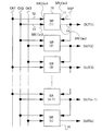
図1に示すように、回路10はn個(nは2以上の自然数)の回路SR(1)〜SR(n)を直列に接続して、シフトレジスタ回路を構成している。
As shown in FIG. 1, the
入力端子11は、1段目の回路10であるSR(1)ではスタートパルスを入力し、2段目以降の回路10は前段の出力端子14からの出力を入力するための入力端子である。入力端子12は、1段目の回路10であるSR(1)ではクロック信号であるCK1、2段目の回路10であるSR(2)ではクロック信号であるCK2、3段目の回路10であるSR(3)ではクロック信号CK3、4段目の回路10であるSR(4)ではCK1というようにCK1、CK2、及びCK3を順に入力する入力端子である。
The
入力端子13は、1段目の回路10であるSR(1)ではCK2、2段目の回路10であるSR(2)ではCK3、3段目の回路10であるSR(3)ではCK1、4段目の回路10であるSR(4)ではCK2というようにCK1、CK2、及びCK3を順に入力する入力端子である。出力端子14は、回路10の出力端子であり、1段目の回路10であるSR(1)ではOUT(1)を出力して、且つ2段目の回路10であるSR(2)の入力端子11にOUT(1)を出力し、2段目の回路10であるSR(2)ではOUT(2)を出力して、且つ3段目の回路10であるSR(3)の入力端子11にOUT(2)を出力する。なお、入力端子11〜14は、それぞれ配線に接続されている。
The
ここで、SSP、CK1、CK2、及びCK3は、HighとLowの2値の値を持つ1ビットの信号である。また、OUT(1)、OUT(2)、OUT(3)、OUT(n−1)、及びOUT(n)も、HighとLowの2値の値を持つ1ビットの出力である。Highは正電源であるVDDと同一の電位であり、Lowは負電源であるVSSと同一の電位である。 Here, SSP, CK1, CK2, and CK3 are 1-bit signals having binary values of High and Low. OUT (1), OUT (2), OUT (3), OUT (n-1), and OUT (n) are also 1-bit outputs having binary values of High and Low. High is the same potential as VDD which is a positive power source, and Low is the same potential as VSS which is a negative power source.
図1のシフトレジスタ回路の動作について、図2に示す本実施形態のタイミングチャートを参照して説明する。 The operation of the shift register circuit of FIG. 1 will be described with reference to the timing chart of the present embodiment shown in FIG.
図2において、SSPは任意のタイミングでパルス幅がCK1、CK2及びCK3の1/3周期となるHighのスタートパルスである。CK1、CK2、及びCK3は3相のクロック信号である。また、図1において、CK3がHighとなるときにSSPもHighとなることが望ましい。nodeP(1)は、後に説明する図3のnodePの電位である。OUT(1)は1段目の回路10であるSR(1)の出力であり、OUT(2)は2段目の回路10であるSR(2)の出力であり、OUT(3)は3段目の回路10であるSR(3)の出力であり、OUT(n−1)はn−1段目の回路10であるSR(n−1)の出力であり、OUT(n)はn段目の回路10であるSR(n)の出力である。
In FIG. 2, SSP is a high start pulse whose pulse width is 1/3 of CK1, CK2 and CK3 at an arbitrary timing. CK1, CK2, and CK3 are three-phase clock signals. Further, in FIG. 1, it is desirable that SSP also becomes High when CK3 becomes High. nodeP (1) is a potential of nodeP in FIG. 3 to be described later. OUT (1) is the output of SR (1) which is the
図2のタイミングチャートに示すように、期間T1においてSSPがHighとなると、期間T2においてOUT(1)がHighとなり、期間T3においてOUT(2)がHighとなる。こうして、SSPの出力をシフトすることによってシフトレジスタ回路を構成している。 As shown in the timing chart of FIG. 2, when SSP becomes High in the period T1, OUT (1) becomes High in the period T2, and OUT (2) becomes High in the period T3. Thus, the shift register circuit is configured by shifting the output of the SSP.
次に、図3を参照して、1段目の回路10の構成について説明する。
Next, the configuration of the first-
図3に示す回路10は、入力端子11、入力端子12、入力端子13、出力端子14、トランジスタ31、トランジスタ32、容量素子33、回路34、回路35から構成されている。なお、入力端子11〜13は、それぞれ配線に接続されている。入力端子11、入力端子12、入力端子13、出力端子14は、図1で説明したものと同様なものとする。トランジスタ31及びトランジスタ32は、Nチャネル型トランジスタであり、非結晶半導体、多結晶半導体、若しくは単結晶半導体によって構成されている。容量素子33は、2つの電極を持つ容量素子である。回路34は、CK2がHighの場合にnodePにLowを出力し、CK2がLowの場合に出力がフローティングになる機能を有する回路である。回路35は、CK2がHighの場合に出力端子14にLowを出力し、CK2がLowの場合に出力がフローティングになる機能を有する回路である。
3 includes an
図3の接続関係について説明する。トランジスタ31のゲートは入力端子11と接続され、ソースとドレインのうち一方はVDDと接続され、ソースとドレインのうち他方は容量素子33の一方の電極、トランジスタ32のゲート及び回路34の出力端子、つまりnodePと接続されている。また、トランジスタ32のソースとドレインのうち一方は入力端子12と接続され、ソースとドレインのうち他方は回路35の出力端子、容量素子33の他方の端子及び出力端子14と接続されている。入力端子13は回路34の入力端子及び回路35の入力端子と接続されている。
The connection relationship in FIG. 3 will be described. The gate of the
図3の動作について、図2に示す本実施形態のタイミングチャートを参照して、期間T1、期間T2及び期間T3に分けて説明する。また、初期状態として、nodeP及びOUT(1)の電位はVSSとする。 The operation of FIG. 3 will be described by dividing it into a period T1, a period T2, and a period T3 with reference to the timing chart of the present embodiment shown in FIG. In addition, as an initial state, the potentials of nodeP and OUT (1) are VSS.
期間T1において、SSPがHigh、CK1がLow、CK2がLow、CK3がHighとなる。このときのトランジスタ31のゲートの電位はVDD、ソースとドレインのうち一方の電位はVDD、ソースとドレインのうち他方の電位はVSSとなるため、当該トランジスタ31がオンして、nodePの電位がVSSから上昇し始める。nodePの電位の上昇は、VDDからトランジスタ31のしきい値電圧分小さい電位となるところで止まり、トランジスタ31はオフする。このときのnodePの電位をVn1とする。また、回路34及び回路35は、CK2がLowとなっているため、出力はフローティングとなる。そのため、nodePには電荷が供給されないため、フローティングとなる。このときのトランジスタ32のゲートの電位はVn1、ソースとドレインのうち一方の電位はVSS、ソースとドレインのうち他方の電位はVSSとなるため、当該トランジスタ32は、オンしている。しかし、ソースとドレインのうち一方の電位とソースとドレインのうち他方の電位とが同電位であり、電荷の移動はないため、電流は流れず、電位も変動しない。そして、容量素子33は出力端子14の電位であるVSSとnodePの電位であるVn1との電位差を保持している。
In the period T1, SSP is High, CK1 is Low, CK2 is Low, and CK3 is High. At this time, the potential of the gate of the
期間T2において、SSPがLow、CK1がHigh、CK2がLow、CK3がLowとなる。このときのトランジスタ31のゲートの電位はVSS、ソースとドレインのうち一方の電位はVDD、ソースとドレインのうち他方の電位はVn1となるため、当該トランジスタ31はオフする。回路34及び回路35は、CK2がLowとなっているため、出力はフローティングとなる。このときのトランジスタ32のゲートの電位はVn1、ソースとドレインのうち一方の電位はVDD、ソースとドレインのうち他方、つまり出力端子14の電位はVSSとなるため、当該トランジスタ32がオンして、出力端子14の電位が上昇し始める。すると、トランジスタ32のゲートと、ソースとドレインのうち他方の間に接続されている容量素子33は、期間T1で保持した電位差をそのまま保持するため、ソースとドレインのうち他方の電位が上昇すると、ゲート電圧も同時に上昇する。このときの、nodePの電位をVn2とする。nodePの電位がVDDとトランジスタ32のしきい値電圧との和まで上昇すると、出力端子14の電位の上昇はCK1と同じVDDになるところで止まる。いわゆる、ブートストラップ動作によって、CK1のHighの電位であるVDDまで、出力端子14の電位を上昇することができる。
In the period T2, SSP is Low, CK1 is High, CK2 is Low, and CK3 is Low. At this time, the potential of the gate of the
期間T3において、SSPがLow、CK1がLow、CK2がHight、CK3がLowとなる。このとき、nodePの電位は、CK2がHighであり、回路34からVSSが出力されるためVSSとなり、OUT(1)の電位も回路35からVSSが出力されるためVSSとなる。このときのトランジスタ31のゲート電位はVSS、ソースとドレインのうち一方の電位はVDD、ソースとドレインのうち他方の電位はVSSとなり、当該トランジスタ31はオフする。トランジスタ32のゲートの電位はVss、ソースとドレインのうち一方の電位はVSS、ソースとドレインのうち他方の電位はVSSとなり、当該トランジスタ32はオフする。
In the period T3, SSP is Low, CK1 is Low, CK2 is High, and CK3 is Low. At this time, the potential of nodeP is VSS because CK2 is High and VSS is output from the
上記説明した期間T1、期間T2、期間T3の動作により、期間T1にSSPが入力されるとOUT(1)が期間T2に出力される。つまり、SSPがクロック信号の1/3周期ずつシフトして出力される回路10をn段接続することにより、シフトレジスタ回路を構成している。
When SSP is input in the period T1, OUT (1) is output in the period T2 by the operations in the above-described periods T1, T2, and T3. In other words, the shift register circuit is configured by connecting n stages of the
図3においては、1段目の回路10であるSR(1)を示したが、n段目の回路10であるSR(n)について図51を参照して説明する。図51において、トランジスタ31、トランジスタ32、容量素子33、回路34、回路35、入力端子11、入力端子12、入力端子13、及び出力端子14は図3で説明したものと同様なものとする。入力端子11から入力される入力信号は前の段の回路10の出力端子14と接続されていることを特徴とする。
In FIG. 3, SR (1) which is the
なお、トランジスタ31のゲート及びトランジスタ32のソースとドレインのうち他方は電源線となる配線(以下、「電源線」と記す)と接続してもよく、例えば正電源VDD、負電源VSSなどの電源線、又は他の電源線と接続してもよいし、他の信号線となる配線(以下、「信号線」と記す)と接続してもよい。また、トランジスタ31のソースとドレインのうち他方は信号線と接続してもよく、例えばCK1、CK2、CK3、SSPなどの信号線、又は他の信号線と接続してもよいし、他の電源線と接続してもよい。
Note that the other of the gate of the
図3に示したシフトレジスタ回路で用いたトランジスタはNチャネル型トランジスタのみで構成する単極性回路であったが、Pチャネル型トランジスタのみで構成してもよい。もちろん、Pチャネル型トランジスタとNチャネル型トランジスタ組み合わせてもよい。トランジスタを全てPチャネル型トランジスタで構成した場合のシフトレジスタ回路について図55を参照して説明する。 Although the transistor used in the shift register circuit shown in FIG. 3 is a unipolar circuit composed of only N-channel transistors, it may be composed of only P-channel transistors. Of course, a P-channel transistor and an N-channel transistor may be combined. A shift register circuit in which all transistors are P-channel transistors will be described with reference to FIG.
図55に示す回路構成において、正電源VDD、負電源VSS、入力端子11、入力端子12、入力端子13、出力端子14は図3と同様なものを用いることができる。トランジスタ551、及びトランジスタ552はPチャネル型トランジスタであり、非結晶半導体、多結晶半導体、若しくは単結晶半導体によって構成されている。容量素子553は2つの電極を持つ容量素子である。回路554はCK2がLowの場合にnodePにHighを出力し、CK2がHighの場合に出力がフローティングとなる機能を有する回路である。回路555はCK2がLowの場合に出力端子14にHighを出力し、CK2がHighの場合に出力がフローティングとなる機能を有する回路である。
In the circuit configuration shown in FIG. 55, the positive power supply VDD, the negative power supply VSS, the
図55の接続関係について説明する。トランジスタ551のゲートは入力端子11と接続され、ソースとドレインのうち一方は正電源VSSと接続され、ソースとドレインのうち他方は容量素子553の一方の電極、トランジスタ552のゲート及び回路554の出力端子、つまりnodePと接続されている。トランジスタ552のソースとドレインのうち一方は入力端子12と接続され、ソースとドレインのうち他方は回路555の出力端子、容量素子553の他方の電極、及び出力端子14と接続されている。入力端子13は回路554の入力端子、及び回路555の入力端子と接続されている。
The connection relationship in FIG. 55 will be described. The gate of the
なお、トランジスタ551のゲート及びトランジスタ552のソースとドレインのうち他方は電源線と接続してもよく、例えば正電源VDD、負電源VSSなどの電源線、又は他の電源線と接続してもよいし、他の信号線と接続してもよい。また、トランジスタ551のソースとドレインのうち他方は信号線と接続してもよく、例えばCK1、CK2、CK3、SSPなどの信号線、又は他の信号線と接続してもよいし、他の電源線と接続してもよい。
Note that the other of the gate of the
図59(a)を参照して、図55に示す回路554の構成の一例について説明する。図59(a)に示す回路554に示すように、入力端子13、及びnodePは図55と同様なものとする。トランジスタ591はPチャネル型トランジスタであり、非結晶半導体、多結晶半導体、若しくは単結晶半導体によって構成されている。
An example of the structure of the
図59(a)の接続関係について説明する。トランジスタ591のゲートは入力端子13と接続され、ソースとドレインのうち一方はVDDと接続され、ソースとドレインのうち他方はnodePと接続されている。
The connection relationship in FIG. 59 (a) will be described. The gate of the
図59(a)の動作について説明する。入力端子13から入力されるCK2がLowの場合に、トランジスタ591はオンして、nodePにVDDを出力し、CK2がHighの場合に、トランジスタ591はオフして、nodePにはなにも出力されない。こうして、回路554は、CK2がLowの場合にHighを出力して、Highの場合にはフローティングになる機能を有する回路を構成している。また、回路構成は説明した回路構成に限らず、同じ機能を有する回路構成であればよい。
The operation of FIG. 59 (a) will be described. When CK2 input from the
なお、トランジスタ591のソースとドレインのうち一方は信号線に接続してもよく、例えばCK1、CK2、CK3、SSPなどの信号線、又は他の信号線と接続してもよいし、他の電源線と接続してもよい。また、トランジスタ591のゲートは電源線と接続してもよく、例えば正電源VDD、負電源VSSなどの電源線、又は他の電源線と接続してもよいし、他の信号線と接続してもよい。
Note that one of a source and a drain of the
図59(b)を参照して、図55に示す回路555の構成の一例について説明する。図59(b)に示す回路555に示すように、入力端子13、及び出力端子14は図55と同様なものとする。トランジスタ592はPャネル型トランジスタであり、非結晶半導体、多結晶半導体、若しくは単結晶半導体によって構成されている。
An example of the structure of the
図59(b)の動作について説明する。入力端子13から入力されるCK2がLowの場合に、トランジスタ592はオンして、出力端子14にVDDを出力し、CK2がHighの場合に、トランジスタ592はオフして、出力端子14にはなにも出力されない。こうして、回路555は、CK2がLowの場合にHighを出力して、Highの場合にはフローティングになる機能を有する回路を構成している。また、回路構成は説明した回路構成に限らず、同じ機能を有する回路構成であればよい。
The operation of FIG. 59B will be described. When CK2 input from the
なお、トランジスタ592のソースとドレインのうち一方は信号線に接続してもよく、例えばCK1、CK2、CK3、SSPなどの信号線、又は他の信号線と接続してもよいし、他の電源線と接続してもよい。また、トランジスタ592のゲートは電源線と接続してもよく、例えば正電源VDD、負電源VSSなどの電源線、又は他の電源線と接続してもよいし、他の信号線と接続してもよい。
Note that one of a source and a drain of the
次に、図4(a)を参照して、図3に示す回路34の構成の一例について説明する。
Next, an example of the configuration of the
図4(a)に示す回路34において、入力端子13、及びnodePは図3と同様なものとする。トランジスタ41はNチャネル型トランジスタであり、非結晶半導体、多結晶半導体、若しくは単結晶半導体によって構成されている。
In the
図4(a)の接続関係について説明する。トランジスタ41のゲートは入力端子13と接続され、ソースとドレインのうち一方はVSSと接続され、ソースとドレインのうち他方はnodePと接続されている。
The connection relationship in FIG. 4A will be described. The gate of the
図4(a)の動作について説明する。入力端子13から入力されるCK2がHighの場合に、トランジスタ41はオンして、nodePにVSSを出力し、CK2がLowの場合に、トランジスタ41はオフして、nodePにはなにも出力されない。こうして、回路34は、CK2がHighの場合にLowを出力して、Lowの場合にはフローティングになる機能を有する回路を構成している。また、回路構成は説明した回路構成に限らず、同じ機能を有する回路構成であればよい。
The operation of FIG. 4A will be described. When CK2 input from the
なお、トランジスタ41のソースとドレインのうち一方は信号線に接続してもよく、例えばCK1、CK2、CK3、SSPなどの信号線、又は他の信号線と接続してもよいし、他の電源線と接続してもよい。また、トランジスタ41のゲートは電源線と接続してもよく、例えば正電源VDD、負電源VSSなどの電源線、又は他の電源線と接続してもよいし、他の信号線と接続してもよい。
Note that one of the source and the drain of the
図4(b)を参照して、図3に示す回路35の構成の一例について説明する。
An example of the configuration of the
図4(b)に示す回路35において、入力端子13、及び出力端子14は図3と同様なものとする。トランジスタ42はNチャネル型トランジスタであり、非結晶半導体、多結晶半導体、若しくは単結晶半導体によって構成されている。
In the
図4(b)の動作について説明する。入力端子13から入力されるCK2がHighの場合に、トランジスタ42はオンして、出力端子14にVSSを出力し、CK2がLowの場合に、トランジスタ42はオフして、出力端子14にはなにも出力されない。こうして、回路35は、CK2がHighの場合にLowを出力して、Lowの場合にはフローティングになる機能を有する回路を構成している。また、回路構成は説明した回路構成に限らず、同じ機能を有する回路構成であればよい。
The operation of FIG. 4B will be described. When CK2 input from the
なお、トランジスタ42のソースとドレインのうち一方は、信号線に接続してもよく、例えばCK1、CK2、CK3、SSPなどの信号線、又は他の信号線と接続してもよいし、他の電源線と接続してもよい。もちろん、トランジスタ42のソースとドレインのうち一方をトランジスタ41のソースとドレインのうち一方が接続されたVSSとなる配線と接続してもよい。また、トランジスタ42のゲートは電源線と接続してもよく、例えば正電源VDD、負電源VSSなどの電源線、又は他の電源線と接続してもよいし、他の信号線と接続してもよい。
Note that one of the source and the drain of the
つまり、図3、図4に示す構造は、第1のトランジスタ(トランジスタ31)と、第2のトランジスタ(トランジスタ32)と、第3のトランジスタ(トランジスタ41)と、第4のトランジスタ(トランジスタ42)とを有し、第1のトランジスタは、ソースとドレインのうち一方が第1の配線(VDD)に接続され、ソースとドレインのうち他方が第2のトランジスタのゲート電極と第3のトランジスタのソースとドレインのうち他方に接続され、ゲート電極が第5の配線(入力端子11)に接続され、第2のトランジスタは、ソースとドレインのうち一方が第3の配線(入力端子12)に接続され、ソースとドレインのうち他方が第6の配線(出力端子14)に接続され、第3のトランジスタは、ソースとドレインのうち一方が第2の配線(VSS)に接続され、ソースとドレインのうち他方が第2のトランジスタのゲート電極に接続され、ゲート電極が第4の配線(入力端子13)に接続され、第4のトランジスタは、ソースとドレインのうち一方が第2の配線(VSS)に接続され、ソースとドレインのうち他方が第6の配線(出力端子14)に接続され、ゲート電極が第4の配線(入力端子13)に接続されている。また、第1のトランジスタにおいて、ソースとドレインのうち一方を第5の配線(入力端子11)に接続させた構成とすることも可能である。 That is, the structure shown in FIGS. 3 and 4 includes the first transistor (transistor 31), the second transistor (transistor 32), the third transistor (transistor 41), and the fourth transistor (transistor 42). The first transistor has one of a source and a drain connected to the first wiring (VDD), and the other of the source and the drain is the gate electrode of the second transistor and the source of the third transistor. And the drain are connected to the other, the gate electrode is connected to the fifth wiring (input terminal 11), and the second transistor has one of the source and drain connected to the third wiring (input terminal 12). The other of the source and the drain is connected to the sixth wiring (output terminal 14), and the third transistor has one of the source and the drain connected to the second wiring. The other of the source and drain is connected to the gate electrode of the second transistor, the gate electrode is connected to the fourth wiring (input terminal 13), and the fourth transistor is connected to the line (VSS). One of the drains is connected to the second wiring (VSS), the other of the source and drain is connected to the sixth wiring (output terminal 14), and the gate electrode is connected to the fourth wiring (input terminal 13). Has been. In the first transistor, one of the source and the drain can be connected to the fifth wiring (input terminal 11).
以上のような、シフトレジスタ回路では、CK2がHighになるに従って、nodeP、及び出力端子14にVSSを供給することができる。つまり、非選択期間に、一定期間毎にVSSを入力することによって、ノイズを減らすことができ、且つ定常的にオンするトランジスタがないため、特性が劣化することを抑制することができる。また、最低で4つのトランジスタで動作することがきるため、シフトレジスタ回路全体としての素子数を減らすことができ、絶縁基板上に少ない面積で内部回路を構成することが可能となる。
In the shift register circuit as described above, VSS can be supplied to the node P and the
以下に、本実施形態の変更可能な構成例、及び動作例をいくつか述べる。また、以下で述べる構成例、及び動作例は「課題を解決するための手段」、「発明を実施するための最良の形態」、及び「実施例」について適用可能である。 Hereinafter, some configuration examples and operation examples of the embodiment that can be changed will be described. The configuration examples and operation examples described below can be applied to “means for solving the problems”, “best mode for carrying out the invention”, and “examples”.
図1に示すように、CK1、CK2、及びCK3のクロック信号は、回路10が非選択期間の場合にも入力されているが、スイッチ素子などを設けて、非選択期間の回路10へ入力しなくしてもよい。こうすることで、クロック信号線の負荷が減るため、消費電力を小さくすることができる。
As shown in FIG. 1, the clock signals of CK1, CK2, and CK3 are input even when the
また、図1において、上記説明したシフトレジスタ回路を逆向きに走査させてもよい。例えば、n段目の回路10の出力をn−1段目の回路10に入力すればよい。これを全段で繰り返すことで、逆向きに走査することが可能である。
In FIG. 1, the shift register circuit described above may be scanned in the reverse direction. For example, the output of the
図2に示すように、SSP、CK1、CK2、CK3のパルス幅を1/3周期としたが、パルス幅を1/3周期より少し短くしてもよい。こうすることで、貫通電流などの瞬間的に流れる電流を抑制でき、広い動作条件で動作することができ、且つ消費電力を小さくすることができる。また、ブートストラップ動作を行う回路構成においては、浮遊となるノードが発生するため、正常なブートストラップ動作を行うためにも有利である。 As shown in FIG. 2, the pulse width of SSP, CK1, CK2, and CK3 is set to 1/3 period, but the pulse width may be slightly shorter than 1/3 period. By doing so, current that flows instantaneously such as a through current can be suppressed, operation can be performed under a wide range of operating conditions, and power consumption can be reduced. Further, in a circuit configuration that performs a bootstrap operation, a floating node is generated, which is advantageous for performing a normal bootstrap operation.
図2において、SSPがHighとなる期間は、CK3がHighとなる期間及びパルス幅を同一としたが、これに限るものではない。例えば、制御信号によって、外部回路から内部回路へ信号を伝達する場合に、バッファ回路、信号振幅を変えるレベルシフト回路などによって制御信号どうしの遅延時間が変わる可能性があるためである。 In FIG. 2, the period during which SSP is High is the same as the period during which CK3 is High and the pulse width, but the present invention is not limited to this. For example, when a signal is transmitted from an external circuit to an internal circuit by a control signal, the delay time between the control signals may be changed by a buffer circuit, a level shift circuit that changes the signal amplitude, or the like.
図3において、容量素子33は、ブートストラップ動作をするために接続されており、トランジスタ32のゲートと、ソースとドレインのうち他方との間にブートストラップ動作できるだけのゲートとソース間の容量などがあれば、なくてもよい。また、容量素子33の形成方法はなんでもよい。例えば、半導体層とゲート配線層との間で容量素子を形成してもよいし、非結晶半導体層と配線との間で容量素子を形成してもよい。半導体層とゲート配線層とで容量素子を形成する場合は、ボトムゲートトランジスタ、トップゲート型トランジスタに関らず薄いGI膜(ゲート絶縁膜)を挟んで形成されているため、小さい面積でより多くの容量値を得ることが可能となるため、有利である。
In FIG. 3, a
また、図3において、SSPはトランジスタ31のゲートに入力したが、トランジスタ31のゲートと、ソースとドレインのうち一方とを接続して、そこにSSPを入力してもよい。こうすることで、正電源VDDが必要なくなり電源線を1本減らすことができるため、シフトレジスタ回路を形成するための面積を小さくすることができる。その結果、より高精細、且つ狭額縁な表示装置を提供することが可能となる。
In FIG. 3, the SSP is input to the gate of the
図3に示した回路34及び回路35は、上記で説明したように、CK2がHighの場合にVSSを出力し、CK2がLowの場合にフローティングとなる回路であればよい。また、回路34の入力端子に次の段の回路10の出力を入力してもよいし、同様に回路35の入力端子には次の段の回路10の出力を入力してもよいし、回路34の入力端子、及び回路35の入力端子に次の段の回路10の出力を入力してもよい。次の段の回路10の出力を利用することで、制御信号だけに同期するのではなく実際のシフトレジスタ回路の出力とも同期することができるため、よりシフトレジスタ回路の動作にあった電位の切り替えができるため有利である。
As described above, the
図3に示すように、nodePと、VSS又はVDDの間に容量素子を接続してもよい。容量素子を接続することでより、nodePの電位を安定させることができる。 As shown in FIG. 3, a capacitor may be connected between nodeP and VSS or VDD. By connecting the capacitor, the potential of the node P can be stabilized.
なお、図3において、回路34は必ずしも必要ではない。つまり、回路35によって、一定期間毎にVSSを出力しているため、nodePにノイズがあってもトランジスタ32をオフしていればよいためである。こうすることで、素子数を減らすことができる。そのとき、nodePとVSS、又はVDDの間に容量素子を接続してもよい。
In FIG. 3, the
(第2の実施形態)
本実施形態は、非選択期間の出力電圧のノイズを減らすために、一定時間毎にVSSを出力することでノイズを減らすことを特徴とするシフトレジスタ回路の構成、及び動作について、図2、図5乃至図7を用いて説明する。
(Second Embodiment)
In this embodiment, in order to reduce noise in the output voltage during the non-selection period, the noise is reduced by outputting VSS at regular time intervals, and the configuration and operation of the shift register circuit, which is characterized in that FIG. This will be described with reference to FIGS.
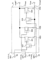
図5に示すように、回路50はn個(nは2以上の自然数)の回路SR(1)〜SR(n)を直列に接続して、シフトレジスタ回路を構成している。
As shown in FIG. 5, the
入力端子51は、1段目の回路50であるSR(1)ではスタートパルスを入力し、2段目以降の回路50であるSR(2)では前段の出力端子55からの出力を入力するための入力端子である。入力端子52は、1段目の回路50であるSR(1)ではクロック信号であるCK1、2段目の回路50であるSR(2)ではクロック信号であるCK2、3段目の回路50であるSR(3)ではクロック信号CK3、4段目の回路50であるSR(4)ではCK1というようにクロック信号を順に入力する入力端子である。入力端子53は、1段目の回路50であるSR(1)ではCK2、2段目の回路50であるSR(2)ではCK3、3段目の回路50であるSR(3)ではCK1、4段目の回路50であるSR(4)ではCK2というようにクロック信号を順に入力する入力端子である。入力端子54は、1段目の回路50であるSR(1)ではCK3、2段目の回路50であるSR(2)ではCK1、3段目の回路50であるSR(3)ではCK2、4段目の回路50であるSR(4)ではCK3というようにクロック信号を順に入力する入力端子である。出力端子55は、回路50の出力端子であり、1段目の回路50あるSR(1)ではOUT(1)を出して、且つ2段目の回路50であるSR(2)の入力端子51にOUT(1)を出力し、2段目の回路50であるSR(2)ではOUT(2)を出力して、且つ3段目の回路50であるSR(3)の入力端子51にOUT(2)を出力する。
The
ここで、SSP、CK1、CK2及びCK3は、HighとLowの2値の値を持つ1ビットの信号である。Highは正電源であるVDDと同一の電位であり、Lowは負電源であるVSSと同一の電位である。ここで、SSP、CK1、CK2及びCK3は、HighとLowの2値の値を持つ1ビットの信号である。また、OUT(1)、OUT(2)、OUT(3)、OUT(n−1)及びOUT(n)も、HighとLowの2値の値を持つ1ビットの出力である。Highは正電源であるVDDと同一の電位であり、Lowは負電源であるVSSと同一の電位である。 Here, SSP, CK1, CK2, and CK3 are 1-bit signals having binary values of High and Low. High is the same potential as VDD which is a positive power source, and Low is the same potential as VSS which is a negative power source. Here, SSP, CK1, CK2, and CK3 are 1-bit signals having binary values of High and Low. OUT (1), OUT (2), OUT (3), OUT (n−1), and OUT (n) are also 1-bit outputs having binary values of High and Low. High is the same potential as VDD which is a positive power source, and Low is the same potential as VSS which is a negative power source.
図5のシフトレジスタ回路の動作について、図2に示す本実施形態のタイミングチャートを参照して説明する。 The operation of the shift register circuit of FIG. 5 will be described with reference to the timing chart of the present embodiment shown in FIG.
SSP、CK1、CK2及びCK3は第1の実施形態と同様のものを用いることができる。なお、nodeP(1)は、後に説明する図6のnodePの電位である。OUT(1)は1段目の回路50であるSR(1)の出力であり、OUT(2)は2段目の回路50であるSR(2)の出力であり、OUT(3)は3段目の回路50であるSR(3)の出力であり、OUT(n−1)はn−1段目の回路50であるSR(n−1)の出力であり、OUT(n)はn段目の回路50であるSR(n)の出力である。
SSP, CK1, CK2, and CK3 can be the same as those in the first embodiment. Note that nodeP (1) is the potential of nodeP in FIG. OUT (1) is the output of SR (1) which is the
図2のタイミングチャートにおいて、期間T1においてSSPがHighとなると、期間T2においてOUT(1)がHighとなり、期間T3においてOUT(2)がHighとなる。こうして、SSPの出力をシフトすることによってシフトレジスタ回路を構成している。 In the timing chart of FIG. 2, when SSP becomes High in the period T1, OUT (1) becomes High in the period T2, and OUT (2) becomes High in the period T3. Thus, the shift register circuit is configured by shifting the output of the SSP.
次に、図6を参照して、1段目の回路50の構成について説明する。
Next, the configuration of the first-
図6に示す回路50は、入力端子51、入力端子52、入力端子53、入力端子54、出力端子55、トランジスタ31、トランジスタ32、容量素子33、回路34、回路35から構成されている。入力端子51、入力端子52、入力端子53、入力端子54、出力端子55は図5で説明したものと同様なものとする。トランジスタ31、トランジスタ32及びnodePは図3で説明したものと同様なものとする。回路61は、CK2がHighの場合にnodePにLowを出力し、CK2がLowの場合に出力がフローティングになる機能を有する回路である。回路62は、CK2及びCK3のいずれかがHighの場合に出力端子55にLowを出力し、CK2及びCK3がLowの場合に出力がフローティングになる機能を有する回路である。
The
図6の接続関係について説明する。トランジスタ31のゲートは入力端子51と接続され、ソースとドレインのうち一方はVDDと接続され、ソースとドレインのうち他方は容量素子33の一方の電極、トランジスタ32のゲート及び回路61の出力端子、つまりnodePと接続されている。トランジスタ32のソースとドレインのうち一方は入力端子52と接続され、ソースとドレインのうち他方は回路62の出力端子、容量素子33の他方の電極及び出力端子55と接続されている。入力端子53は回路61の入力端子及び回路62の入力端子と接続され、入力端子54は回路62の入力端子と接続されている。
The connection relationship in FIG. 6 will be described. The gate of the
図6の動作について、図2に示す本実施形態のタイミングチャートを参照して、期間T1、期間T2、及び期間T3に分けて説明する。また、初期状態として、nodeP、及びOUT(1)の電位はVSSとする。 The operation of FIG. 6 will be described by dividing it into a period T1, a period T2, and a period T3 with reference to the timing chart of the present embodiment shown in FIG. Further, as an initial state, the potentials of nodeP and OUT (1) are VSS.
期間T1において、SSPがHigh、CK1がLow、CK2がLow、CK3がHighとなる。このときのトランジスタ31のゲートの電位はVDD、ソースとドレインのうち一方の電位はVDD、ソースとドレインのうち他方の電位はVSSとなるため、当該トランジスタ31がオンして、nodePの電位がVSSから上昇し始める。nodePの電位の上昇はVDDからトランジスタ31のしきい値電圧分小さい電位となるところで止まり、トランジスタ31はオフする。このときのnodePの電位をVn1とする。回路61は、CK2がLowとなっているため、出力はフローティングとなる。そのため、nodePには電荷が供給されないため、フローティングとなる。回路62は、CK2がLow、CK3がHighとなっているため、Lowを出力する。このときのトランジスタ32のゲート電位はVn1、ソースとドレインのうち一方の電位はVSS、ソースとドレインのうち他方の電位はVSSとなるため、当該トランジスタ32はオンしている。しかし、ソースとドレインのうち一方の電位とソースとドレインのうち他方の電位とが同電位であり、電荷の移動はないため、電流は流れず、電位も変動しない。そして、容量素子33は出力端子55の電位であるVSSとnodePの電位であるVn1との電位差を保持している。
In the period T1, SSP is High, CK1 is Low, CK2 is Low, and CK3 is High. At this time, the potential of the gate of the
期間T2において、SSPがLow、CK1がHigh、CK2がLow、CK3がLowとなる。このときのトランジスタ31のゲートの電位はVSS、ソースとドレインのうち一方の電位はVDD、ソースとドレインのうち他方の電位はVn1となるため、当該トランジスタ31はオフする。回路61ではCK2がLowとなっているため、出力はフローティングとなる。回路62ではCK2がLow、CK3がLowとなっているため、出力はフローティングとなる。このときのトランジスタ32のゲートの電位はVn1、ソースとドレインのうち一方の電位はVDD、ソースとドレインのうち他方、つまり出力端子55の電位はVSSとなるため、当該トランジスタ32はオンして、出力端子55の電位が上昇し始める。すると、トランジスタ32のゲートと、ソースとドレインのうち他方の間に接続されている容量素子33は期間T1で保持した電位差をそのまま保持するため、ソースとドレインのうち他方の電位が上昇すると、ゲート電圧も同時に上昇する。このときの、nodePの電位をVn2とする。nodePの電位がVDDとトランジスタ32のしきい値電圧との和まで上昇すれば、出力端子14の電位の上昇はCK1と同じVDDになるところで止まる。いわゆる、ブートストラップ動作によって、CK1のHighの電位であるVDDまで、出力端子55の電位を上昇することができる。
In the period T2, SSP is Low, CK1 is High, CK2 is Low, and CK3 is Low. At this time, the potential of the gate of the
期間T3において、SSPがLow、CK1がLow、CK2がHigh、CK3がLowとなる。このとき、nodePの電位は、CK2がHighであるため、回路61からVSSが出力されるため、VSSとなり、OUT(1)の電位も回路62からVSSが出力されるため、VSSとなる。このときのトランジスタ31のゲート電位はVSS、ソースとドレインのうち一方の電位はVDD、ソースとドレインのうち他方の電位はVSSとなり、当該トランジスタ31はオフする。トランジスタ32のゲートの電位はVSS、ソースとドレインのうち一方の電位はVSS、ソースとドレインのうち他方の電位はVSSとなり、当該トランジスタ32はオフする。
In the period T3, SSP is Low, CK1 is Low, CK2 is High, and CK3 is Low. At this time, the potential of nodeP becomes VSS because VSS is output from the
上記説明した期間T1、期間T2、期間T3の動作により、期間T1にSSPが入力されるとOUT(1)が期間T2に出力される。つまり、SSPがクロック信号の1/3周期ずつシフトして出力される回路50をn段接続することにより、シフトレジスタ回路を構成している。
When SSP is input in the period T1, OUT (1) is output in the period T2 by the operations in the above-described periods T1, T2, and T3. That is, the shift register circuit is configured by connecting n stages of
図6に示した1段目の回路50を示したが、n段目の回路50を図52を参照して説明する。図52において、トランジスタ31、トランジスタ32、容量素子33、回路61、回路62、入力端子51、入力端子52、入力端子53、入力端子54、及び出力端子55は図6で説明したものと同様なものとする。入力端子51から入力される入力信号は前の段の回路の出力端子55と接続されていることを特徴とする。
Although the first-
なお、トランジスタ31のゲート、及びトランジスタ32のソースとドレインのうち他方は電源線と接続してもよく、例えば正電源VDD、負電源VSSなどの電源線、又は他の電源線と接続してもよいし、他の信号線と接続してもよい。また、トランジスタ31のソースとドレインのうち他方は信号線と接続してもよく、例えばCK1、CK2、CK3、SSPなどの信号線、又は他の信号線と接続してもよいし、他の電源線と接続してもよい。
Note that the gate of the
図6に示したシフトレジスタ回路で用いたトランジスタはNチャネル型トランジスタのみで構成する単極性回路であったが、Pチャネル型トランジスタのみで構成してもよい。もちろん、Pチャネル型トランジスタとNチャネル型トランジスタ組み合わせてもよい。トランジスタを全てPチャネル型トランジスタで構成した場合のシフトレジスタ回路を図56を参照して説明する。 Although the transistor used in the shift register circuit shown in FIG. 6 is a unipolar circuit composed of only N-channel transistors, it may be composed of only P-channel transistors. Of course, a P-channel transistor and an N-channel transistor may be combined. A shift register circuit in the case where all transistors are P-channel transistors will be described with reference to FIG.
図56に示す回路構成において、正電源VDD、負電源SS、入力端子51、入力端子52、入力端子53、入力端子54、トランジスタ551、トランジスタ552、及び容量素子553は図55と同様なものを用いることができる。回路561は、CK2がLowの場合にnodePにHighを出力し、CK2がHighの場合に出力がフローティングとなる機能を有する回路である。回路562は、CK2、及びCK3のいずれかがLowの場合にnodePにHighを出力し、CK2、及びCK3がHIghの場合に出力がフローティングとなる機能を有する回路である。
56, the positive power supply VDD, the negative power supply SS, the
図56の接続関係について説明する。トランジスタ551のゲートは入力端子51と接続され、ソースとドレインのうち一方は正電源VSSと接続され、ソースとドレインのうち他方は容量素子553の一方の電極、トランジスタ552のゲート及び回路561の出力端子、つまりnodePと接続されている。トランジスタ552のソースとドレインのうち一方は入力端子52と接続され、ソースとドレインのうち他方は回路562の出力端子、容量素子553の他方の電極及び出力端子55接続されている。入力端子53は回路561の入力端子及び回路562の第1の入力端子と接続され、入力端子54は回路562の第1のトランジスタの第2の入力端子と接続されている。
The connection relationship in FIG. 56 will be described. The gate of the
なお、トランジスタ551のゲート、及びトランジスタ552のソースとドレインのうち他方は電源線と接続してもよく、例えば正電源VDD、負電源VSSなどの電源線又は他の電源線と接続してもよいし、他の信号線と接続してもよい。また、トランジスタ551のソースとドレインのうち他方は信号線と接続してもよく、例えばCK1、CK2、CK3、SSPなどの信号線、又は他の信号線と接続してもよいし、他の電源線と接続してもよい。
Note that the other of the gate of the
次に、図60(a)を参照して、図56に示す回路561の構成の一例について説明する。
Next, an example of the configuration of the
図60(a)に示す回路561において、入力端子53、及びnodePは図55と同様なものとする。トランジスタ601はPチャネル型トランジスタであり、非結晶半導体、多結晶半導体、若しくは単結晶半導体によって構成されている。
In the
図60(a)の接続関係について説明する。トランジスタ601のゲートは、入力端子53と接続され、ソースとドレインのうち一方はVDDと接続され、ソースとドレインのうち他方はnodePと接続されている。
The connection relationship in FIG. 60A will be described. The gate of the
図60(a)の動作について説明する。入力端子53から入力されるCK2がLowの場合に、トランジスタ601はオンして、nodePにVDDを出力し、CK2がHighの場合に、トランジスタ601はオフして、nodePにはなにも出力されない。こうして、回路561は、CK2がLowの場合にHighを出力して、Highの場合にはフローティングになる機能を有する回路を構成している。また、回路構成は説明した回路構成に限らず、同じ機能を有する回路構成であればよい。
The operation of FIG. 60A will be described. When CK2 input from the
なお、トランジスタ601のソースとドレインのうち一方は信号線に接続してもよく、例えばCK1、CK2、CK3、SSPなどの信号線、又は他の信号線と接続してもよいし、他の電源線と接続してもよい。また、トランジスタ601のゲートは電源線と接続してもよく、例えば正電源VDD、負電源VSSなどの電源線、又は他の電源線と接続してもよいし、他の信号線と接続してもよい。
Note that one of the source and the drain of the
図60(b)を参照して、図56に示す回路562の構成の一例について説明する。
An example of the structure of the
図60(b)に示す回路562において、入力端子53、54、及び出力端子55は図55と同様なものとする。トランジスタ602、603はPャネル型トランジスタであり、非結晶半導体、多結晶半導体、若しくは単結晶半導体によって構成されている。
In the
図60(b)の動作について説明する。入力端子53から入力されるCK2がLowの場合に、トランジスタ602はオンして、出力端子55にVDDを出力し、CK2がHighの場合に、トランジスタ602はオフして、出力端子55にはなにも出力されない。入力端子54から入力されるCK3がLowの場合にトランジスタ603はオンして、出力端子55にVDDを出力し、CK3がHighの場合に出力端子55にはなにも出力されない。こうして、回路562は、CK2、CK3のいずれかががLowの場合にHighを出力して、Highの場合にはフローティングになる機能を有する回路を構成している。また、回路構成は説明した回路構成に限らず、同じ機能を有する回路構成であればよい。
The operation of FIG. 60B will be described. When CK2 input from the
なお、トランジスタ592のソースとドレインのうち一方は信号線に接続してもよく、例えばCK1、CK2、CK3、SSPなどの信号線、又は他の信号線と接続してもよいし、他の電源線と接続してもよい。また、トランジスタ592のゲートは電源線と接続してもよく、例えば正電源VDD、負電源VSSなどの電源線、又は他の電源線と接続してもよいし、他の信号線と接続してもよい。
Note that one of a source and a drain of the
次に、図7(a)を参照して、図6に示す回路61の構成の一例について説明する。
Next, an example of the configuration of the
図7(a)に示す回路61に示すように、入力端子53、及びnodePは図6と同様なものとする。トランジスタ71はNチャネル型トランジスタであり、非結晶半導体、多結晶半導体、若しくは単結晶半導体によって構成されている。
As shown in the
図7(a)の接続関係について説明する。トランジスタ71のゲートは入力端子53と接続され、ソースとドレインのうち一方はVSSと接続され、ソースとドレインのうち他方はnodePと接続されている。
The connection relationship in FIG. 7A will be described. The gate of the
図7(a)の動作について説明する。入力端子53から入力されるCK2がHighの場合に、トランジスタ71はオンして、nodePにVSSを出力し、CK2がLowの場合に、トランジスタ71はオフして、nodePにはなにも出力されない。こうして、回路61は、CK2がHighの場合にLowを出力して、Lowの場合にはフローティングになる機能を有する回路を構成している。また、回路構成は説明した回路構成に限らず、同じ機能を有する回路構成であればよい。
The operation of FIG. 7A will be described. When CK2 input from the
なお、トランジスタ71のソースとドレインのうち一方は信号線に接続してもよく、例えばCK1、CK2、CK3、SSPなどの信号線、又は他の信号線と接続してもよいし、他の電源線と接続してもよい。また、トランジスタ71のゲートは電源線と接続してもよく、例えば正電源VDD、負電源VSSなどの電源線、又は他の電源線と接続してもよいし、他の信号線と接続してもよい。
Note that one of the source and the drain of the
図7(b)を参照して、図6に示す回路62の構成の一例について説明する。
An example of the configuration of the
図7(b)に示す回路62に示すように、入力端子53、入力端子54及びOUT(1)は図6と同様なものとする。トランジスタ72、及びトランジスタ73はNチャネル型トランジスタであり、非結晶半導体、多結晶半導体、若しくは単結晶半導体によって構成されている。
As shown in the
図7(b)の接続関係について説明する。トランジスタ72のゲートは入力端子53と接続され、ソースとドレインのうち一方はVSSと接続され、ソースとドレインのうち他方は出力端子55と接続されている。トランジスタ73のゲートは入力端子54と接続され、ソースとドレインのうち一方はVSSと接続され、ソースとドレインのうち他方は出力端子55と接続されている。もちろん、トランジスタ72及びトランジスタ73のソースとドレインのうち一方を、トランジスタ71のソースとドレインのうち一方が接続されたVSSとなる配線と接続してもよい。
The connection relationship in FIG. 7B will be described. The gate of the
図7(b)の動作について説明する。入力端子53から入力されるCK2がHighの場合に、トランジスタ72はオンして、OUT(1)にVSSを出力し、CK2がLowの場合に、トランジスタ72はオフしてOUT(1)にはなにも出力されない。また、入力端子54から入力されるCK3がHighの場合に、トランジスタ73はオンして、OUT(1)にVSSを出力し、CK3がLowの場合に、トランジスタ73はオフしてOUT(1)にはなにも出力されない。こうして、回路62は、CK2及びCK3のいずれかがHighの場合にOUT(1)にLowを出力し、CK2及びCK3がLowの場合にはフローティングになる機能を有する回路を構成している。また、回路構成は説明した回路構成に限らず、同じ機能を有する回路構成であればよい。
The operation of FIG. 7B will be described. When CK2 input from the
なお、トランジスタ72のソースとドレインのうち一方、及びトランジスタ73のソースとドレインの一方は信号線に接続してもよく、例えばCK1、CK2、CK3、SSPなどの信号線、又は他の信号線と接続してもよいし、他の電源線と接続してもよい。また、トランジスタ72のゲートは電源線と接続してもよく、例えば正電源VDD、負電源VSSなどの電源線、又は他の電源線と接続してもよいし、他の信号線と接続してもよい。また、トランジスタ73のゲートは電源線と接続してもよく、例えば正電源VDD、負電源VSSなどの電源線、又は他の電源線と接続してもよいし、他の信号線と接続してもよい。
Note that one of the source and the drain of the
つまり、図6、図7に示す構造は、第1のトランジスタ(トランジスタ31)と、第2のトランジスタ(トランジスタ32)と、第3のトランジスタ(トランジスタ71)と、第4のトランジスタ(トランジスタ72)と、第5のトランジスタ(トランジスタ73)とを有し、第1のトランジスタは、ソースとドレインのうち一方が第1の配線(VDD)に接続され、ソースとドレインのうち他方が第2のトランジスタのゲート電極と第3のトランジスタのソースとドレインのうち他方に接続され、ゲート電極が第5の配線(入力端子51)に接続され、第2のトランジスタは、ソースとドレインのうち一方が第3の配線(入力端子52)に接続され、ソースとドレインのうち他方が第6の配線(出力端子55)に接続され、第3のトランジスタは、ソースとドレインのうち一方が第2の配線(VSS)に接続され、ソースとドレインのうち他方が第2のトランジスタのゲート電極に接続され、ゲート電極が第4の配線(入力端子53)に接続され、第4のトランジスタは、ソースとドレインのうち一方が第2の配線(VSS)に接続され、ソースとドレインのうち他方が第6の配線(出力端子55)に接続され、ゲート電極が第4の配線(入力端子53)に接続され、第5のトランジスタは、ソースとドレインのうち一方が第2の配線(VSS)に接続され、ソースとドレインのうち他方が第6の配線(出力端子55)に接続され、ゲート電極が第7の配線(入力端子54)に接続されている。また、第1のトランジスタにおいて、ソースとドレインのうち一方を第5の配線(入力端子51)に接続させた構成とすることも可能である。 That is, the structure shown in FIGS. 6 and 7 includes the first transistor (transistor 31), the second transistor (transistor 32), the third transistor (transistor 71), and the fourth transistor (transistor 72). And a fifth transistor (transistor 73). One of the source and drain of the first transistor is connected to the first wiring (VDD), and the other of the source and drain is the second transistor. The gate electrode is connected to the other of the source and drain of the third transistor, the gate electrode is connected to the fifth wiring (input terminal 51), and one of the source and drain of the second transistor is the third one. The other of the source and drain is connected to the sixth wiring (output terminal 55), and the third transistor is connected to the third wiring (input terminal 52). One of the source and drain is connected to the second wiring (VSS), the other of the source and drain is connected to the gate electrode of the second transistor, and the gate electrode is connected to the fourth wiring (input terminal 53). The fourth transistor has one of a source and a drain connected to the second wiring (VSS), and the other of the source and the drain connected to a sixth wiring (output terminal 55), and a gate The electrode is connected to the fourth wiring (input terminal 53), and the fifth transistor has one of the source and the drain connected to the second wiring (VSS), and the other of the source and the drain is the sixth wiring. The gate electrode is connected to the seventh wiring (input terminal 54). In the first transistor, one of a source and a drain can be connected to a fifth wiring (input terminal 51).
以上のような、シフトレジスタ回路では、CK2及びCK3のいずれかがHighになるに従って、出力端子55にVSSを供給することができる。つまり、非選択期間に、一定期間毎にVSSを入力することによって、ノイズを減らすことができ、且つ定常的にオンするトランジスタがないため、特性が劣化することを抑制することができる。また、第1の実施形態に比べ、非選択期間に示すように2倍の期間、VSSを出力端子55に供給することができるため、よりノイズを低減することができる。
In the shift register circuit as described above, VSS can be supplied to the
以下に、本実施形態の変更可能な構成例、及び動作例をいくつか述べる。また、以下で述べる構成例、及び動作例は「課題を解決するための手段」、「発明を実施するための最良の形態」、及び「実施例」について適用可能であり、第1の実施形態で説明した変更可能な構成例、及び動作例を本実施形態に適用することができる。 Hereinafter, some configuration examples and operation examples of the embodiment that can be changed will be described. In addition, the configuration example and the operation example described below are applicable to “means for solving the problem”, “best mode for carrying out the invention”, and “example”, and are described in the first embodiment. The changeable configuration example and operation example described in the above can be applied to the present embodiment.
図6に示すように、nodePと、VSS又はVDDの間に容量素子を接続してもよい。容量素子を接続することでより、nodePの電位を安定させることができる。 As illustrated in FIG. 6, a capacitor may be connected between nodeP and VSS or VDD. By connecting the capacitor, the potential of the node P can be stabilized.
図6に示すように、容量素子33はブートストラップ動作をするために接続されており、トランジスタ32のゲートと、ソースとドレインのうち他方との間にブートストラップ動作できるだけの寄生容量などがあれば、なくてもよい。また、容量素子33の形成方法はどこでもよい。例えば、非結晶半導体層とゲート配線層との間で容量素子を形成してもよいし、半導体層と配線との間で容量素子を形成してもよい。半導体層とゲート配線層とで容量素子を形成する場合は、ボトムゲートトランジスタ、トップゲート型トランジスタに関らず薄いGI膜(ゲート絶縁膜)を挟んで形成されているため、小さい面積でより多くの容量値を得ることが可能となるため、有利である。
As shown in FIG. 6, the
図6に示すように、回路61は必ずしも必要ではない。つまり、回路62によって、一定期間毎にVSSを出力しているため、nodePにノイズがあってもトランジスタ32をオフしていればよいためである。こうすることで、素子数を減らすことができる。そのとき、nodePと、VSS又はVDDの間に容量素子を接続してもよい。
As shown in FIG. 6, the
図6に示した回路62の入力端子に次の段の回路50の出力を入力してもよいし、同様に回路35の入力端子には次の段の回路50の出力を入力してもよいし、回路61の入力端子、及び回路62の入力端子に次の段の回路50の出力を入力してもよい。次の段の回路50の出力を利用することで、制御信号だけに同期するのではなく実際のシフトレジスタ回路の出力とも同期することができるため、よりシフトレジスタ回路の動作にあった電位の切り替えができるため有利である。
The output of the
図6に示すように、nodePとVSS、又はVDDの間に容量素子を接続してもよい。容量素子を接続することでより、nodePの電位を安定させることができる。 As shown in FIG. 6, a capacitor may be connected between nodeP and VSS or VDD. By connecting the capacitor, the potential of the node P can be stabilized.
(第3の実施形態)
本実施形態は、非選択期間の出力電圧のノイズを減らすために、非選択期間においてVSSを出力することでノイズを減らすことを特徴とするシフトレジスタ回路の構成、及び動作について、図2、図5、図8乃至図10を用いて説明する。
(Third embodiment)
In this embodiment, in order to reduce noise in the output voltage during the non-selection period, the noise is reduced by outputting VSS in the non-selection period. 5 and FIG. 8 to FIG.
図5に示すシフトレジスタ回路の構成、及び動作は第2の実施形態で説明したものと同様なものを用いることができる。 The structure and operation of the shift register circuit shown in FIG. 5 can be the same as those described in the second embodiment.
図8を参照して、1段目の回路50であるSR(1)の構成について説明する。図8に示す回路50は、入力端子51、入力端子52、入力端子53、入力端子54、出力端子55、トランジスタ31、トランジスタ32、容量素子33、回路81、回路82、回路83から構成されている。
With reference to FIG. 8, the configuration of SR (1) which is the
入力端子51、入力端子52、入力端子53、入力端子54、出力端子55、トランジスタ31、トランジスタ32、容量素子33は、図5で説明したものと同様なものとする。
The
回路81は、CK2がHighの場合にnodePにLowを出力し、CK2がLowの場合に出力がフローティングになる機能を有する回路である。回路82は、回路83の出力がHighで、且つCK1、CK2及びCK3のいずれかがHighの場合に出力端子55にLowを出力し、CK1、CK2及びCK3がLowの場合に出力がフローティングになる。そして、回路83からの出力がLowで、且つCK2及びCK3のいずれかがHighの場合に出力端子55にLowを出力し、CK2及びCK3がLowの場合に出力がフローティングとなる機能を有する回路である。回路83は、nodePの電位がVDD付近、もしくはそれ以上の場合に回路82にLowを出力し、nodePの電位がVSSの場合に回路82にHighを出力する回路である。
The
図8の接続関係について説明する。トランジスタ31のゲートは入力端子51と接続され、ソースとドレインのうち一方はVDDと接続され、ソースとドレインのうち他方は容量素子33の一方の電極、トランジスタ32のゲート、回路83の入力端子及び回路81の出力端子、つまりnodePと接続されている。トランジスタ32のソースとドレインのうち一方は入力端子52と接続され、ソースとドレインのうち他方は回路82の出力端子、容量素子33の他方の端子、及び出力端子55と接続されている。入力端子52は回路82の入力端子と接続され、入力端子53は回路81の入力端子、及び回路82の入力端子と接続され、入力端子54は回路82の入力端子と接続されている。回路83の出力端子は回路82の入力端子と接続されている。
The connection relationship in FIG. 8 will be described. The gate of the
図8の動作について、図2に示す本実施形態のタイミングチャートを参照して、期間T1、期間T2、及び期間T3に分けて説明する。また、初期状態として、nodeP、及びOUT(1)の電位はVSSとする。 The operation of FIG. 8 will be described by dividing it into a period T1, a period T2, and a period T3 with reference to the timing chart of the present embodiment shown in FIG. Further, as an initial state, the potentials of nodeP and OUT (1) are VSS.
期間T1において、SSPがHigh、CK1がLow、CK2がLow、CK3がHighとなる。このときのトランジスタ31のゲートの電位はVDD、ソースとドレインのうち一方の電位はVDD、ソースとドレインのうち他方の電位はVSSとなるため、当該トランジスタ31がオンして、nodePの電位がVSSから上昇し始める。nodePの電位の上昇はVDDからトランジスタ31のしきい値電圧分小さい電位となるところで止まり、トランジスタ31はオフする。このときのnodePの電位をVn1とする。回路81は、CK2がLowとなっているため、出力はフローティングとなる。そのため、nodePには電荷が供給されないため、フローティングとなる。回路83は、nodePの電位がVn1となるため、回路82の入力端子にLowを出力する。回路82は、回路83の出力がLow、CK1がLow、CK2がLow、CK3がHighとなるため、Lowを出力する。このときのトランジスタ32のゲート電位はVn1、ソースとドレインのうち一方の電位はVSS、ソースとドレインのうち他方の電位はVSSとなるため、当該トランジスタ32はオンしている。しかし、ソースとドレインのうち一方の電位とソースとドレインのうち他方の電位とが同電位であり、電荷の移動はないため、電流は流れず、電位も変動しない。そして、容量素子33には出力端子55の電位であるVSSとnodePの電位であるVn1との電位差を保持している。
In the period T1, SSP is High, CK1 is Low, CK2 is Low, and CK3 is High. At this time, the potential of the gate of the
期間T2において、SSPがLow、CK1がHigh、CK2がLow、CK3がLowとなる。このときのトランジスタ31のゲートの電位はVSS、ソースとドレインのうち一方の電位はVDD、ソースとドレインのうち他方の電位はVn1となるため、当該トランジスタ31はオフする。回路61ではCK2がLowとなっているため、出力はフローティングなる。回路83は、nodePの電位がVn1となるため回路82の入力端子にLowを出力する。回路82は、回路83の出力がLow、CK1がHigh、CK2がLow、CK3がLowとなるため、出力はフローティングとなる。このときのトランジスタ32のゲートの電位はVn1、ソースとドレインのうち一方の電位はVDD、ソースとドレインのうち他方、つまり出力端子55の電位はVSSとなるため、当該トランジスタ32がオンして、出力端子55の電位が上昇し始める。すると、トランジスタ32のゲートと、ソースとドレインのうち他方の間に接続されている容量素子33は期間T1で保持した電位差をそのまま保持するため、ソースとドレインのうち他方の電位が上昇すると、ゲート電圧も同時に上昇する。このときの、nodePの電位をVn2とする。nodePの電位がVDDとトランジスタ32のしきい値電圧との和まで上昇すれば、出力端子55の電位の上昇はCK1の電位と同じVDDになるところで止まる。いわゆる、ブートストラップ動作によって、CK1のHighの電位であるVDDまで、出力端子55の電位を上昇することができる。
In the period T2, SSP is Low, CK1 is High, CK2 is Low, and CK3 is Low. At this time, the potential of the gate of the
期間T3において、SSPがLow、CK1がLow、CK2がHight、CK3がLowとなる。このとき、nodePの電位は、CK2がHighであるため、回路81からVSSが出力されるため、VSSとなり、回路83は回路82の入力端子にHighを出力する。OUT(1)の電位も回路82からVSSが出力されるため、VSSとなる。このときのトランジスタ31のゲート電位はVSS、ソースとドレインのうち一方の電位はVDD、ソースとドレインのうち他方の電位はVSSとなり、当該トランジスタ31はオフする。トランジスタ32のゲートの電位はVSS、ソースとドレインのうち一方の電位はVSS、ソースとドレインのうち他方の電位はVSSとなり、当該トランジスタ32はオフする。
In the period T3, SSP is Low, CK1 is Low, CK2 is High, and CK3 is Low. At this time, the potential of nodeP is VSS because CK <b> 2 is High and VSS is output from the
上記説明した期間T1、期間T2、期間T3の動作により、期間T1にSSPが入力されるとOUT(1)が期間T2に出力される。つまり、SSPがクロック信号の1/3周期ずつシフトして出力される回路50をn段接続することにより、シフトレジスタ回路を構成している。
When SSP is input in the period T1, OUT (1) is output in the period T2 by the operations in the above-described periods T1, T2, and T3. That is, the shift register circuit is configured by connecting n stages of
図8に1段目の回路50を示したが、n段目の回路50を図53を参照して説明する。
Although the
図53において、トランジスタ31、トランジスタ32、容量素子33、回路81、回路82、回路83、入力端子51、入力端子52、入力端子53、入力端子54及び出力端子55は、図8で説明したものと同様なものとする。入力端子51から入力される入力信号は前の段の回路の出力端子55と接続されていることを特徴とする。
53, the
図8に示したシフトレジスタ回路で用いたトランジスタはNチャネル型トランジスタのみで構成する単極性回路であったが、Pチャネル型トランジスタのみで構成してもよい。もちろん、Pチャネル型トランジスタとNチャネル型トランジスタ組み合わせてもよい。トランジスタを全てPチャネル型トランジスタで構成した場合のシフトレジスタ回路を図57を参照して説明する。 Although the transistor used in the shift register circuit shown in FIG. 8 is a unipolar circuit composed of only N-channel transistors, it may be composed of only P-channel transistors. Of course, a P-channel transistor and an N-channel transistor may be combined. A shift register circuit in the case where all transistors are P-channel transistors will be described with reference to FIG.
図57に示す回路構成において、正電源VDD、負電源SS、入力端子51、入力端子52、入力端子53、入力端子54、トランジスタ551、トランジスタ552、及び容量素子553は図55と同様なものを用いることができる。回路571は、CK2がLowの場合にnodePにHighを出力し、CK2がHighの場合に出力がフローティングとなる機能を有する回路である。回路572はCK1、CK2、CK3のうちいずれかがLowのときに出力端子55にHighを出力する回路である。
In the circuit configuration shown in FIG. 57, the positive power supply VDD, the negative power supply SS, the
図57の接続関係について説明する。トランジスタ551のゲートは入力端子51と接続され、ソースとドレインのうち一方は正電源VSSと接続され、ソースとドレインのうち他方は容量素子553の一方の電極、トランジスタ552のゲート及び回路571の出力端子、つまりnodePと接続されている。トランジスタ552のソースとドレインのうち一方は入力端子52と接続され、ソースとドレインのうち他方は回路572の出力端子、容量素子553の他方の電極、及び出力端子55と接続されている。入力端子52は回路572の入力端子と接続されている。入力端子53は回路571の入力端子、及び回路572の第1の入力端子と接続され、入力端子54は回路572の第1のトランジスタの第2の入力端子と接続されている。
The connection relationship in FIG. 57 will be described. The gate of the
なお、トランジスタ551のゲート及びトランジスタ552のソースとドレインのうち他方は電源線と接続してもよく、例えば正電源VDD、負電源VSSなどの電源線、又は他の電源線と接続してもよいし、他の信号線と接続してもよい。また、トランジスタ551のソースとドレインのうち他方は信号線と接続してもよく、例えばCK1、CK2、CK3、SSPなどの信号線、又は他の信号線と接続してもよいし、他の電源線と接続してもよい。
Note that the other of the gate of the
次に、図9(a)を参照して、図8に示す回路81の構成の一例について説明する。
Next, an example of the configuration of the
図9(a)に示す回路81において、入力端子53、及びnodePは図8と同様なものとする。トランジスタ91はNチャネル型トランジスタであり、非結晶半導体、多結晶半導体、若しくは単結晶半導体によって構成されている。
In the
図9(a)の接続関係について説明する。トランジスタ91のゲートは入力端子53と接続され、ソースとドレインのうち一方はVSSと接続され、ソースとドレインのうち他方はnodePと接続されている。
The connection relationship in FIG. 9A will be described. The gate of the transistor 91 is connected to the
図9(a)の動作について説明する。入力端子53から入力されるCK2がHighの場合に、トランジスタ91はオンして、nodePにVSSを出力し、CK2がLowの場合に、トランジスタ91はオフして、nodePにはなにも出力されない。こうして、回路81は、CK2がHighの場合にLowを出力して、Lowの場合にはフローティングになる機能を有する回路を構成している。また、回路構成は説明した回路構成に限らず、同じ機能を有する回路構成であればよい。また、Pチャネル型トランジスタで構成した場合の構成例を図61に示す。同業者であれば容易に変更が可能である。
The operation of FIG. 9A will be described. When CK2 input from the
なお、トランジスタ91のソースとドレインのうち一方は信号線に接続してもよく、例えばCK1、CK2、CK3、SSPなどの信号線、又は他の信号線と接続してもよいし、他の電源線と接続してもよい。また、トランジスタ91のゲートは電源線と接続してもよく、例えば正電源VDD、負電源VSSなどの電源線、又は他の電源線と接続してもよいし、他の信号線と接続してもよい。 Note that one of the source and the drain of the transistor 91 may be connected to a signal line. For example, the transistor 91 may be connected to a signal line such as CK1, CK2, CK3, or SSP, another signal line, or another power source. You may connect with a line. The gate of the transistor 91 may be connected to a power supply line. For example, the transistor 91 may be connected to a power supply line such as a positive power supply VDD or a negative power supply VSS, or another power supply line, or may be connected to another signal line. Also good.
図9(b)を参照して、図8に示す回路82の構成の一例について説明する。
With reference to FIG. 9B, an example of the configuration of the
図9(b)に示す回路82において、入力端子52、入力端子53、入力端子54及びOUT(1)は図8と同様なものとする。トランジスタ92、トランジスタ93、トランジスタ94及びトランジスタ95はNチャネル型トランジスタであり、非結晶半導体、多結晶半導体、若しくは単結晶半導体によって構成されている。Voutは回路82の出力である。
In the
図9(b)の接続関係について説明する。トランジスタ95のゲートはVoutが接続され、ソースとドレインのうち一方は入力端子52と接続され、ソースとドレインのうち他方はトランジスタ92のゲートと接続されている。トランジスタ92のソースとドレインのうち一方はVSSと接続され、ソースとドレインのうち他方は出力端子55と接続されている。トランジスタ93のゲートは入力端子53と接続され、ソースとドレインのうち一方はVSSと接続され、ソースとドレインのうち他方は出力端子55と接続されている。トランジスタ94のゲートは入力端子54と接続され、ソースとドレインのうち一方はVSSと接続され、ソースとドレインのうち他方は出力端子55と接続されている。
The connection relationship in FIG. 9B will be described. The gate of the
図9(b)の動作について説明する。回路83の出力から入力されるVoutがHighの場合に、トランジスタ95はオンして、トランジスタ92のゲートにCK1を信号を伝達する。VoutがLowの場合に、トランジスタ95はオフして、トランジスタ92のゲートにCK1の信号は伝達されないため、前の状態を保持する。ここで、トランジスタ95がオンして、且つ入力端子52から入力されるCK1がHighの場合に、トランジスタ92はオンして、OUT(1)にVSSを出力し、CK1がLowの場合に、トランジスタ92はオフして、OUT(1)にはなにも出力されない。入力端子53から入力されるCK2がHighの場合に、トランジスタ93はオンして、OUT(1)にVSSを出力し、CK2がLowの場合に、トランジスタ93はオフして、OUT(1)にはなにも出力されない。入力端子54から入力されるCK3がHighの場合に、トランジスタ94がオンして、OUT(1)にVSSが出力され、CK3がLowの場合に、トランジスタ94はオフして、OUT(1)にはなにも出力されない。こうして、回路82は、回路83の出力がHighで、且つCK1、CK2、及びCK3のいずれかがHighの場合に出力端子55にLowを出力し、CK1、CK2、及びCK3がLowの場合に出力がフローティングになる。そして、回路83からの出力がLowで、且つCK2、及びCK3のいずれかがHighの場合に出力端子55にLowを出力し、CK2、及びCK3がLowの場合に出力がフローティングとなる機能を有する回路を構成している。また、回路構成は説明した回路構成に限らず、同じ機能を有する回路構成であればよい。
The operation of FIG. 9B will be described. When Vout input from the output of the
なお、トランジスタ92のソースとドレインのうち一方、トランジスタ93のソースとドレインのうち一方、及びトランジスタ94のソースとドレインのうち一方は信号線に接続してもよく、例えばCK1、CK2、CK3、SSPなどの信号線、又は他の信号線と接続してもよいし、他の電源線と接続してもよい。また、トランジスタ95のソースとドレインのうち一方、トランジスタ92のゲート、トランジスタ93のゲート、トランジス94のゲートは電源線と接続してもよく、例えば正電源VDD、負電源VSSなどの電源線、又は他の電源線と接続してもよいし、他の信号線と接続してもよい。
Note that one of the source and the drain of the
次に、図10(a)を参照して、図8に示す回路83の構成の一例について説明する。
Next, an example of the configuration of the
図10(a)に示す回路83おいて、nodeP、Voutは図8と同様なものとする。トランジスタ101はNチャネル型トランジスタであり、非結晶半導体、多結晶半導体、若しくは単結晶半導体によって構成されている。抵抗素子102は、抵抗成分を持つ抵抗素子である。抵抗成分を持っていれば、いかなる線形素子でもよいし、非線形素子でもよい。例えば、ダイオード接続したトランジスタを接続してもよい。
In the
抵抗素子102として、トランジスタを用いた場合の構成例について図48を参照して説明する。nodeP、Vout、トランジスタ101、正電源線VDD、及び負電源VSSは図10と同様なものとする。トランジスタ481はNチャネル型トランジスタであり、非結晶半導体、多結晶半導体、若しくは単結晶半導体によって構成されている。トランジスタ481のソースとドレインのうち一方は正電源VDDと接続され、ソースとドレインのうち他方はVoutと接続され、ゲートはソースとドレインのうち一方と接続されダイオード接続されている。VoutはVSSからオンするトランジスタ101を介して電荷が供給されなければ、VDDからトランジスタ481のしきい値電圧引いた電位なる。こうして、nodePがLowとなるとトランジスタ101はオフしてVoutの電位はVDDからトランジスタ481のしきい値電圧引いた電位となり、nodePがHighとなりトランジスタ101がオンするとVoutの電位はVSSの電位なる。
A structure example in which a transistor is used as the
図10(a)の接続関係について説明する。トランジスタ101のゲートはnodePと接続され、トランジスタ101のソースとドレインのうち一方は抵抗素子102の一方の端子、及びVoutと接続され、ソースとドレインのうち他方はVSSと接続されている。抵抗素子102の他方の端子はVDDと接続されている。
The connection relationship in FIG. 10A will be described. The gate of the
図10(a)の動作について説明する。nodePの電位がVSSとトランジスタ101のしきい値電圧との和の電圧以上だった場合に、トランジスタ101はオンして、VoutにVSSを出力する。nodePの電位がVSSとトランジスタ101のしきい値電圧との和の電圧未満だった場合に、トランジスタ101はオフして、Voutには抵抗素子102を介してVDDが出力される。このように、nodePの電位がVSSとトランジスタ101のしきい値電圧との和の電圧以上だった場合に回路82の入力端子にLowを出力し、nodePの電位がVSSとトランジスタ101のしきい値電圧との和の電圧未満だった場合に回路82の入力端子にHighを出力する機能を有する回路を構成している。また、回路構成は説明した回路構成に限らず、同じ機能を有する回路構成であればよい。また、図62に図10の回路構成をPチャネル型トランジスタを用いた場合の構成例を示す。
The operation of FIG. 10A will be described. When the potential of nodeP is equal to or higher than the sum of VSS and the threshold voltage of the
なお、トランジスタ101のソースとドレインのうち他方は信号線に接続してもよく、例えばCK1、CK2、CK3、SSPなどの信号線、又は他の信号線と接続してもよいし、他の電源線と接続してもよい。また、トランジスタ101のゲートは電源線と接続してもよく、例えば正電源VDD、負電源VSSなどの電源線、又は他の電源線と接続してもよいし、他の信号線と接続してもよい。
Note that the other of the source and the drain of the
図10(b)を参照して、図8に示す回路83の構成の別の一例について説明する。
With reference to FIG. 10B, another example of the configuration of the
図10(b)に示す回路83に示すように、nodeP、Voutは図8と同様なものとする。OUT(2)は次の2段目の回路50の出力である。例えば、n段目の回路50だとするとn+1段目の回路50の出力である。トランジスタ102、及びトランジスタ103はNチャネル型トランジスタであり、非結晶半導体、多結晶半導体、若しくは単結晶半導体によって構成されている。容量素子104は2つの電極を持った容量素子である。
As shown in the
図10(b)の接続関係について説明する。トランジスタ102のゲートはOUT(2)と接続され、ソースとドレインのうち一方はVDDと接続され、ソースとドレインのうち他方はトランジスタ103のソースとドレインのうち一方、容量素子104の一方の電極、及びVoutと接続されている。トランジスタ103のゲートはnodeP、ソースとドレインのうち他方はVSSと接続されている。容量素子104の他方の電極はVSSと接続されている。
The connection relationship in FIG. 10B will be described. The gate of the
図10(b)の動作について説明する。nodePの電位がVSSとトランジスタ103のしきい値電圧との和の電圧以上だった場合に、トランジスタ103はオンしてVSSをVoutに出力する。nodePの電位がVSSとトランジスタ103のしきい値電圧との和の電圧以未満だった場合に、トランジスタ103はオフして出力はフローティングとなる。OUT2がHighだった場合に、トランジスタ102はオンしてVoutにVDDとトランジスタ102のしきい値電圧との差の電圧を出力する。OUT2がLowだった場合に、トランジスタ102はオフして出力はフローティングとなる。つまり、nodePの電位がVDD付近、若しくはそれ以上だった場合に、VoutはLowを出力し、nodePの電位がVSSだった場合に、VoutはHighを出力する機能を有する回路を構成している。また、回路構成は説明した回路構成に限らず、同じ機能を有する回路構成であればよい。
The operation of FIG. 10B will be described. When the potential of nodeP is equal to or higher than the sum of VSS and the threshold voltage of the
なお、トランジスタ102のゲート及びトランジスタ103のゲートは電源線と接続してもよく、例えば正電源VDD、負電源VSSなどの電源線、又は他の電源線と接続してもよいし、他の信号線と接続してもよい。また、トランジスタ103のソースとドレインのうち他方は信号線に接続してもよく、例えばCK1、CK2、CK3、SSPなどの信号線、又は他の信号線と接続してもよいし、他の電源線と接続してもよい。
Note that the gate of the
以上のような、シフトレジスタ回路では、非動作期間において、CK1、CK2及びCK3のうちいずれかがHighとなれば、出力端子55にVSSを供給することができる。つまり、非選択期間における出力端子55には常時VSSが供給されているため、電位が安定し、ノイズを無くすことができ、且つ定常的にオンするトランジスタがないため、特性が劣化することを抑制することができる。また、nodePにも一定期間毎にVSSを供給することによって、トランジスタ32を確実にオフすることができる。
In the shift register circuit as described above, VSS can be supplied to the
以下に、本実施形態の変更可能な構成例、及び動作例をいくつか述べる。また、以下で述べる構成例、及び動作例は「課題を解決するための手段」、「発明を実施するための最良の形態」、及び「実施例」について適用可能であり、第1の実施形態で説明した変更可能な構成例、及び動作例を本実施形態に適用することができる。 Hereinafter, some configuration examples and operation examples of the embodiment that can be changed will be described. In addition, the configuration example and the operation example described below are applicable to “means for solving the problem”, “best mode for carrying out the invention”, and “example”, and are described in the first embodiment. The changeable configuration example and operation example described in the above can be applied to the present embodiment.
図9に示すように、トランジスタ92のゲートは、トランジスタ95がオフのとき浮遊となる。そのため、トランジスタ92のゲート容量に電位を保持しているが、保持しきれない場合は、容量素子を接続してもよい。その場合、トランジスタ92のゲートとVDD、又はVSSとの間に容量素子を接続することが望ましい。
As shown in FIG. 9, the gate of the
図10(b)に示すように、Voutに容量素子104が接続されているが、Voutの接続先が十分な容量をもっていれば設けない構成としてもよい。出力であるVoutに接続されている容量素子104を無くすことで、より高速な動作が可能となる。
As shown in FIG. 10B, the
図10(b)に示すように、トランジスタ103のゲートにはnodePが接続されているが、入力端子51を接続してもよい。入力端子51を接続することによって、トランジスタ102とトランジスタ103とが同時にオンする期間がなくなりトランジスタ102、及びトランジスタ103を介した貫通電流がなくなるため、誤動作しにくくなり、且つ消費電力が小さくなる。
As shown in FIG. 10B, the node P is connected to the gate of the
(第4の実施形態)
本実施形態は、非選択期間の出力電圧のノイズを減らすために、一定時間毎にVSSを出力することでノイズを減らすことを特徴とするシフトレジスタ回路の構成、及び動作について、図2、図5、図11及び図12を用いて説明する。
(Fourth embodiment)
In this embodiment, in order to reduce noise in the output voltage during the non-selection period, the noise is reduced by outputting VSS at regular time intervals, and the configuration and operation of the shift register circuit, which is characterized in that FIG. 5 and FIG. 11 and FIG.
図5に示すシフトレジスタ回路の構成、及び動作は第2の実施形態で説明したものと同様なものを用いることができる。 The structure and operation of the shift register circuit shown in FIG. 5 can be the same as those described in the second embodiment.
図11を参照して、1段目の回路50であるSR(1)の構成について説明する。図11に示す回路は、入力端子51、入力端子52、入力端子53、入力端子54、出力端子55、トランジスタ31、トランジスタ32、容量素子33、回路111、回路82、回路83から構成されている。入力端子51、入力端子52、入力端子53、入力端子54、出力端子55、回路82、回路83、トランジスタ31、トランジスタ32、容量素子33、及びnodePは図8で説明したものと同様なものとする。
With reference to FIG. 11, the configuration of SR (1) which is the
回路111は回路83からの出力がHighの場合で、且つCK1、CK2及びCK3のいずれかがHighの場合にnodePにLowを出力し、CK1、CK2及びCK3がLowの場合に出力がフローティングとなる。そして、回路83からの出力がLowの場合で、且つCK2がHighの場合にnodePにLowを出力し、CK2がLowの場合に出力がフローティングとなる機能を有する回路である。
The
図11接続関係について説明する。トランジスタ31のゲートは入力端子51と接続され、ソースとドレインのうち一方はVDDと接続され、ソースとドレインのうち他方は容量素子33の一方の電極、トランジスタ32のゲート、回路83の入力端子及び回路111の出力端子、つまりnodePと接続されている。トランジスタ32のソースとドレインのうち一方は入力端子52と接続され、ソースとドレインのうち他方は回路82の出力端子、容量素子33の他方の電極、及び出力端子55と接続されている。入力端子52は回路82の入力端子及び回路111の入力端子と接続され、入力端子53は回路82の入力端子及び回路111の入力端子と接続され、入力端子54は回路82の入力端子及び回路111の入力端子と接続されている。回路83の出力端子は回路82の入力端子、及び回路111の入力端子と接続されている。
11 will be described. The gate of the
図11の動作について、図2に示す本実施形態のタイミングチャートを参照して、期間T1、期間T2、及び期間T3に分けて説明する。また、初期状態として、nodeP、及びOUT(1)の電位はVSSとする。 The operation of FIG. 11 will be described by dividing it into a period T1, a period T2, and a period T3 with reference to the timing chart of this embodiment shown in FIG. Further, as an initial state, the potentials of nodeP and OUT (1) are VSS.
期間T1において、SSPがHigh、CK1がLow、CK2がLow、CK3がHighとなる。このときのトランジスタ31のゲートの電位はVDD、ソースとドレインのうち一方の電位はVDD、ソースとドレインのうち他方の電位はVSSとなるため、当該トランジスタ31がオンして、nodePの電位がVSSから上昇し始める。nodePの電位の上昇はVDDからトランジスタ31のしきい値電圧分小さい電位となるところで止まり、トランジスタ31はオフする。このときのnodePの電位をVn1とする。回路83はnodePの電位がVn1となるため、回路82の入力端子、及び回路83の入力端子にLowを出力する。回路111は、回路83の出力がLow、CK1がLow、CK2がLow、CK3がHighなとなるため、出力はフローティングとなる。回路82は、回路83の出力がLow、CK1がLow、CK2がLow、CK3がHighなとなるため出力端子55にLowを出力する。そして、容量素子33には出力端子55の電位であるVSSとnodePの電位であるVn1との電位差が保持されている。
In the period T1, SSP is High, CK1 is Low, CK2 is Low, and CK3 is High. At this time, the potential of the gate of the
期間T2において、SSPがLow、CK1がHigh、CK2がLow、CK3がLowとなる。このときのトランジスタ31のゲートの電位はVSS、ソースとドレインのうち一方の電位はVDD、ソースとドレインのうち他方の電位はVn1となるため、当該トランジスタ31はオフする。回路83はnodePの電位がVn1となるため回路82の入力端子及び回路111の入力端子にLowを出力する。回路111は、回路83の出力がLow、CK1がHigh、CK2がLow、CK3がLowとなるため、出力はフローティングとなる。回路82は、回路83の出力がLow、CK1がHigh、CK2がLow、CK3がLowとなるため、出力はフローティングとなる。このときのトランジスタ32のゲートの電位はVn1、ソースとドレインのうち一方の電位はVDD、ソースとドレインのうち他方、つまり出力端子55の電位はVSSとなるため、当該トランジスタ32がオンして、出力端子55の電位が上昇し始める。すると、トランジスタ32のゲートと、ソースとドレインのうち他方の間に接続されている容量素子33は期間T1で保持した電位差をそのまま保持するため、ソースとドレインのうち他方の電位が上昇すると、ゲートの電位も同時に上昇する。このときの、nodePの電位をVn2とする。nodePの電位がVDDとトランジスタ32のしきい値電圧との和まで上昇すれば、出力端子55の電位の上昇はCK1と同じVDDになるところで止まる。いわゆる、ブートストラップ動作によって、CK1のHighの電位であるVDDまで、出力端子55の電位を上昇することができる。
In the period T2, SSP is Low, CK1 is High, CK2 is Low, and CK3 is Low. At this time, the potential of the gate of the
期間T3において、SSPがLow、CK1がLow、CK2がHight、CK3がLowとなる。このとき、nodePの電位は、CK2がHighであるため、回路111からVSSが出力されるため、VSSとなり、回路83は回路82の入力端子にHighを出力する。OUT(1)の電位も回路82からVSSが出力されるため、VSSとなる。このときのトランジスタ31のゲート電位はVSS、ソースとドレインのうち一方の電位はVDD、ソースとドレインのうち他方の電位はVSSとなり、当該トランジスタ31はオフする。トランジスタ32のゲートの電位はVSS、ソースとドレインのうち一方の電位はVSS、ソースとドレインのうち他方の電位はVSSとなり、当該トランジスタ32はオフする。
In the period T3, SSP is Low, CK1 is Low, CK2 is High, and CK3 is Low. At this time, the potential of the nodeP is VSS because CK2 is High, and VSS is output from the
上記説明した期間T1、期間T2、期間T3の動作により、期間T1にSSPが入力されるとOUT(1)が期間T2に出力される。つまり、SSPがクロック信号の1/3周期ずつシフトして出力される回路50をn段接続することにより、シフトレジスタ回路を構成している。
When SSP is input in the period T1, OUT (1) is output in the period T2 by the operations in the above-described periods T1, T2, and T3. That is, the shift register circuit is configured by connecting n stages of
図11に示したシフトレジスタ回路で用いたトランジスタはNチャネル型トランジスタのみで構成する単極性回路であったが、Pチャネル型トランジスタのみで構成してもよい。もちろん、Pチャネル型トランジスタとNチャネル型トランジスタ組み合わせてもよい。トランジスタを全てPチャネル型トランジスタで構成した場合のシフトレジスタ回路について図58を参照して説明する。 Although the transistor used in the shift register circuit shown in FIG. 11 is a unipolar circuit composed of only N-channel transistors, it may be composed of only P-channel transistors. Of course, a P-channel transistor and an N-channel transistor may be combined. A shift register circuit in which all transistors are P-channel transistors will be described with reference to FIG.
図58に示す回路構成において、正電源VDD,負電源VSS、入力端子51、入力端子52、入力端子53、入力端子54、トランジスタ551、トランジスタ552、及び容量素子553は図55と同様なものを用いることができる。回路572、回路573は図57と同様なものを用いることができる。回路581はCK1、CK2、CK3のうちいずれかがLowのときに出力端子55にHighを出力する回路である。
58, the positive power supply VDD, the negative power supply VSS, the
図58の接続関係について説明する。トランジスタ551のゲートは入力端子51と接続され、ソースとドレインのうち一方は正電源VSSと接続され、ソースとドレインのうち他方は容量素子553の一方の電極、トランジスタ552のゲート及び回路581の出力端子、つまりnodePと接続されている。トランジスタ552のソースとドレインのうち一方は入力端子52と接続され、ソースとドレインのうち他方は回路572の出力端子、容量素子553の他方の電極、及び出力端子55と接続されている。入力端子52は回路572の入力端子と接続されている。入力端子53は回路581の入力端子、及び回路572の第1の入力端子と接続され、入力端子54は回路562の第1のトランジスタの第2の入力端子と接続されている。
The connection relationship in FIG. 58 will be described. The gate of the
なお、トランジスタ551のゲート、及びトランジスタ552のソースとドレインのうち他方は電源線と接続してもよく、例えば正電源VDD、負電源VSSなどの電源線、又は他の電源線と接続してもよいし、他の信号線と接続してもよい。また、トランジスタ551のソースとドレインのうち他方は信号線と接続してもよく、例えばCK1、CK2、CK3、SSPなどの信号線、又は他の信号線と接続してもよいし、他の電源線と接続してもよい。
Note that the other of the gate of the
図11に示した1段目の回路50を示したが、n段目の回路56について図54を参照して説明する。図54において、トランジスタ31、トランジスタ32、容量素子33、回路111、回路82、回路83、入力端子51、入力端子52、入力端子53、入力端子54、及び出力端子55は図11で説明したものと同様なものとする。入力端子51から入力される入力信号は前の段の回路の出力端子55と接続されていることを特徴とする。
Although the first-
次に、図12を参照して、図11に示す回路111の構成の一例について説明する。
Next, an example of the configuration of the
図12に示す回路111に示すように、入力端子52、入力端子53、入力端子54及びOUT(1)は図5及び図11と同様なものとする。トランジスタ121、トランジスタ122、トランジスタ123、トランジスタ124、及びトランジスタ125はNチャネル型トランジスタであり、非結晶半導体、多結晶半導体、若しくは単結晶半導体によって構成されている。Voutは回路111の出力である。
As shown in the
図12の接続関係について説明する。トランジスタ124のゲートはVoutと接続され、トランジスタ124のソースとドレインのうち一方は入力端子52と接続され、ソースとドレインのうち他方はトランジスタ121のゲート接続されている。トランジスタ121のソースとドレインのうち一方はVSSと接続され、ソースとドレインのうち他方はnodePと接続されている。トランジスタ122のゲートは入力端子53と接続され、ソースとドレインのうち一方はVSSと接続され、ソースとドレインのうち他方はnodePと接続されている。トランジスタ125のゲートはVoutと接続され、ソースとドレインのうち一方は入力端子54と接続され、ソースとドレインのうち他方はトランジスタ123のゲートと接続されている。トランジスタ123のソースとドレインのうち一方はVSSと接続され、ソースとドレインのうち他方はnodePと接続されている。
The connection relationship in FIG. 12 will be described. The gate of the
図12の動作について説明する。回路83の出力から入力されるVoutがHighの場合に、トランジスタ124及びトランジスタ125はオンして、トランジスタ121のゲートにCK1の信号を伝達して、トランジスタ123のゲートにCK3の信号を伝達する。VoutがLowの場合に、トランジスタ124及びトランジスタ125はオフして、トランジスタ121のゲートにはCK1の信号は伝達されないため、前の状態を保持して、トランジスタ123のゲートにはCK3の信号が伝達されないため、前の状態を保持する。ここで、トランジスタ124がオンして、且つ入力端子52から入力されるCK1がHighの場合に、トランジスタ121はオンして、nodePにVSSを出力し、CK1がLowの場合に、トランジスタ121はオフして、nodePにはなにも出力されない。入力端子53から入力されるCK2がHighの場合に、トランジスタ122はオンして、nodePにVSSを出力し、CK2がLowの場合に、トランジスタ122はオフして、nodePにはなにも出力されない。トランジスタ125がオンして、且つ入力端子54から入力されるCK3がHighの場合に、トランジスタ123はオンして、nodePにVSSを出力し、CK3がLowの場合に、トランジスタ123はオフして、nodePにはなにも出力されない。こうして、回路111は、回路83の出力がHighで、且つCK1、CK2、及びCK3のいずれかがHighの場合に出力端子55にLowを出力し、CK1、CK2、及びCK3がLowの場合に出力がフローティングになる。そして、回路83からの出力がLowで、且つCK2がHighの場合に出力端子55にLowを出力し、CK2がLowの場合に出力がフローティングとなる機能を有する回路を構成している。また、回路構成は説明した回路構成に限らず、同じ機能を有する回路構成であればよい。また、図63にPチャネルトランジスタを用いた構成例に示している。
The operation of FIG. 12 will be described. When Vout input from the output of the
なお、トランジスタ124のソースとドレインのうち他方、及びトランジスタ121のゲート、トランジスタ122のゲート、トランジスタ125のソースとドレインのうち一方、及びトランジスタ123のゲートは、信号線に接続してもよく、例えばCK1、CK2、CK3、SSPなどの信号線、又は他の信号線と接続してもよいし、他の電源線と接続してもよい。また、トランジスタ121のソースとドレインのうち他方、トランジスタ122のソースとドレインのうち他方、及びトランジスタ123のソースとドレインのうち他方は信号線に接続してもよく、例えばCK1、CK2、CK3、SSPなどの信号線、又は他の信号線と接続してもよいし、他の電源線と接続してもよい。
Note that the other of the source and the drain of the
以上のような、シフトレジスタ回路では、非動作期間において、CK1、CK2及びCK3のうちいずれかがHighとなれば、出力端子55、及びnodePにVSSを供給することができる。つまり、非選択期間における出力端子55、及びnodePには常時VSSが供給されているため、電位が安定し、ノイズを無くすことができ、且つ定常的にオンするトランジスタがないため、特性が劣化することを抑制することができる。
In the shift register circuit as described above, VSS can be supplied to the
以下に、本実施形態の変更可能な構成例、及び動作例をいくつか述べる。また、以下で述べる構成例、及び動作例は「課題を解決するための手段」、「発明を実施するための最良の形態」、及び「実施例」について適用可能であり、第1の実施形態で説明した変更可能な構成例、及び動作例を本実施形態に適用することができる。 Hereinafter, some configuration examples and operation examples of the embodiment that can be changed will be described. In addition, the configuration example and the operation example described below are applicable to “means for solving the problem”, “best mode for carrying out the invention”, and “example”, and are described in the first embodiment. The changeable configuration example and operation example described in the above can be applied to the present embodiment.
図12に示すように、トランジスタ121のゲートに入力される信号は、回路82のトランジスタ92のゲートに入力される信号と共通にしてもよい。こうすることで、トランジスタの数を減らすことができる。
As shown in FIG. 12, the signal input to the gate of the
図12に示すように、トランジスタ121のゲートは、トランジスタ124がオフのとき浮遊となる。そのため、トランジスタ121のゲート容量に電位を保持しているが、保持しきれない場合は、容量素子を接続してもよい。その場合、トランジスタ121のゲートとVDD、又はVSSとの間に容量素子を接続することが望ましい。
As shown in FIG. 12, the gate of the
図12に示すように、トランジスタ123のゲートは、トランジスタ125がオフのとき浮遊となる。そのため、トランジスタ123のゲート容量に電位を保持しているが、保持しきれない場合は、容量素子を接続してもよい。その場合、トランジスタ123のゲートとVDD、又はVSSとの間に容量素子を接続することが望ましい。
As shown in FIG. 12, the gate of the
(第5の実施形態)
本実施形態は、第1の実施形態、乃至第4の実施形態で説明したシフトレジスタ回路を用いた場合の回路の構成の一例についていくつか説明する。
(Fifth embodiment)
In this embodiment, several examples of a circuit configuration in the case of using the shift register circuit described in the first to fourth embodiments are described.
第1の実施形態乃至第4の実施形態で説明したシフトレジスタ回路によって画素を走査するゲートドライバの構成例について図13を参照して説明する。また、そのときのタイミングチャートを図14に示す。 A configuration example of a gate driver that scans pixels with the shift register circuit described in the first to fourth embodiments will be described with reference to FIG. A timing chart at that time is shown in FIG.
図13に示すゲートドライバ回路は第1の実施形態乃至第4の実施形態で説明したシフトレジスタ回路131によって構成されている。そして、ゲート信号線G1乃至ゲート信号線Gnを介して、シフトレジスタ回路131から出力される出力信号であるOUT1乃至OUTnをゲート信号として画素へ伝達する。
The gate driver circuit shown in FIG. 13 includes the
シフトレジスタ回路131は、制御信号であるSSP、CK1、CK2、及びCK3が入力されており、タイミングは図14に示すように第1の実施形態乃至第4の実施形態と同様なものとする。また、電源として正電源VDD及び負電源VSSが入力されており、制御信号の振幅電圧は正電源VDD及び負電源VSSに対応した振幅電圧となっている。図14に示すようにSSPが入力されると、OUT1から順に選択される(以下、走査するともいう)。こうして、シフトレジスタ回路131の出力をそのままゲート信号として、ゲート信号線G1乃至ゲート信号線Gnに出力する。
The
ここで、正電源VDDの電位は後に説明する画素のビデオ信号の最大値よりも高くし、負電源VSSの電位はビデオ信号の最小値よりも低くしておくことが望ましい。こうすることで、ビデオ信号を確実に画素に書き込むことができるため、より高画質な表示装置を提供することができる。 Here, it is desirable that the potential of the positive power supply VDD is higher than the maximum value of the video signal of a pixel described later, and the potential of the negative power supply VSS is lower than the minimum value of the video signal. By doing so, a video signal can be reliably written to a pixel, so that a display device with higher image quality can be provided.
図13で説明したゲートドライバは、シフトレジスタ回路131の出力をそのままゲート信号として出力することを特徴としている。こうすることで、ゲートドライバ部分の面積が小さくなるので有利である。また、ゲートドライバ部分の素子数も少なくなるので、歩留まりを高くすることができるため有利である。
The gate driver described with reference to FIG. 13 is characterized in that the output of the
第1の実施形態乃至第4の実施形態で説明したシフトレジスタ回路の出力信号の振幅電圧を変えて画素を走査するタイプのゲートドライバについて図15を参照して説明する。また、そのときのタイミングチャートを図16に示す。 A gate driver that scans pixels by changing the amplitude voltage of the output signal of the shift register circuit described in the first to fourth embodiments will be described with reference to FIG. FIG. 16 shows a timing chart at that time.
図15に示すゲートドライバ回路は第1の実施形態乃至第4の実施形態で説明したシフトレジスタ回路151及びレベルシフト回路152によって構成されている。そして、ゲート信号線G1乃至ゲート信号線Gnを介して、シフトレジスタ回路151から出力される出力信号であるOUT1乃至OUTnをレベルシフト回路152を介してゲート信号として画素へ伝達する。
The gate driver circuit shown in FIG. 15 includes the
図15に示すレベルシフト回路152を図50(a)及び(b)を参照して説明する。また、図50で説明するレベルシフト回路は図15で示すレベルシフト回路152だけでなく、他の図、発明を実施するための最良の形態、及び実施例に適用することが可能である。
The
図50(a)に示すように、シフトレジスタ回路151のn行目の出力であるOUT(n)と、OUT(n)の振幅電圧の最大値よりも電位が高い電源VDDHと負電源VSSと抵抗成分を含む抵抗素子502とトランジスタ501とをと少なくとも有している。トランジスタ501のゲートはOUT(n)が入力され、ソースとドレインのうち一方は負電源VSSと接続され、ソースとドレインのうち他方は抵抗素子502の一方の端子、及びゲート信号線と接続され、抵抗素子502の他方の端子は電源VDDHと接続されていることを特徴とするレベルシフト回路である。
As shown in FIG. 50A, OUT (n) that is the output of the nth row of the
図50(b)に示すように、シフトレジスタ回路151のn行目の出力であるOUT(n)と、OUT(n)の振幅電圧の最大値よりも電位が高い電源VDDHと負電源VSSとトランジスタ503とトランジスタ504とインバータ回路505とを少なくとも有している。トランジスタ504のゲートはOUT(n)が入力され、トランジスタ503のゲートはOUT(n)がインバータ回路505を介すことで反転したOUT(n)が入力されている。トランジスタ504のソースとドレインのうち一方は負電源VSSと接続され、トランジスタ503のソースとドレインのうち一方は電源VDDと接続されている。トランジスタ504のソースとドレインのうち他方、及びトランジスタ505のソースとドレインのうち他方はゲート信号線と接続されていることを特徴とするレベルシフト回路である。
As shown in FIG. 50B, OUT (n), which is the output of the nth row of the
シフトレジスタ回路151は制御信号であるSSP、CK1、CK2及びCK3が入力されており、タイミングは図16に示すように第1の実施形態乃至第4の実施形態と同様なものとする。また、電源として正電源VDD及び負電源VSSが入力されており、制御信号の振幅電圧は正電源VDD及び負電源VSSに対応した振幅電圧となっている。図16に示すようにSSPが入力されると、OUT1から順に選択される(以下、走査するともいう)。こうして、シフトレジスタ回路151の出力をレベルシフト回路152に入力することができる。また、このときのシフトレジスタ回路151の出力信号の振幅は、Highが正電源VDDの電位であり、Lowが負電源VSSの電位である。
The
レベルシフト回路152は入力されるシフトレジスタ回路151の出力信号の振幅電圧を変化する機能を持つ。例えば、Highが入力された場合は正電源VDDの電位から正電源VDDHの電位、Lowが入力された場合は負電源VSSの電位から負電源VSSLの電位にしてゲート信号線に出力する。また、正電源VDDHの電位は正電源VDDの電位よりも高く、負電源VSSLの電位は負電源VSSの電位よりも低い電位となっている。また、Highのみ振幅電圧を変化させてもよいし、Lowのみの振幅電圧を変化させてもよい。
The
ここで、正電源VDDHの電位は後に説明する画素に入力するビデオ信号の最大値よりも高くし、負電源VSSの電位はビデオ信号の最小値よりも低くしておくことが望ましい。こうすることで、ビデオ信号を確実に画素に書き込むことができるため、より高画質な表示装置を提供することができる。 Here, it is desirable that the potential of the positive power supply VDDH be higher than the maximum value of a video signal input to a pixel, which will be described later, and the potential of the negative power supply VSS be lower than the minimum value of the video signal. By doing so, a video signal can be reliably written to a pixel, so that a display device with higher image quality can be provided.
図15で説明したゲートドライバは、シフトレジスタ回路151の出力信号をレベルシフト回路152を介すことで、振幅電圧を変化させてゲート信号線に出力することを特徴としている。こうすることで、シフトレジスタ回路151は小さい振幅電圧の制御信号、及び電源で駆動することができ、消費電力を小さくすることができるため有利である。
The gate driver described with reference to FIG. 15 is characterized in that the output voltage of the
第1の実施形態乃至第4の実施形態で説明したシフトレジスタ回路に入力する制御信号をレベルシフト回路を介してシフトレジスタ回路に入力するタイプのゲートドライバについて図17を参照して説明する。また、そのときのタイミングチャートを図18に示す。 A gate driver of a type in which a control signal input to the shift register circuit described in the first to fourth embodiments is input to the shift register circuit through the level shift circuit will be described with reference to FIG. A timing chart at that time is shown in FIG.
図17に示すゲートドライバ回路は、第1の実施形態乃至第4の実施形態で説明したシフトレジスタ回路171及びレベルシフト回路172によって構成されている。そして、ゲート信号線G1乃至ゲート信号線Gnを介して、シフトレジスタ回路151から出力される出力信号であるOUT1乃至OUTnをゲート信号として画素へ伝達する。
The gate driver circuit shown in FIG. 17 includes the
レベルシフト回路172は入力される信号の振幅電圧を変化するための回路である。例えば、入力される信号のHighの電位をシフトレジスタ回路171の電源である正電源VDDの電位に変化させ、Lowの電位を負電源VSSの電位に変えることができる。図17の場合はレベルシフト回路172に入力される制御信号SSP、CK1、CK2及びCK3の振幅電圧を正電源VDD、及び負電源VSSに対応した振幅電圧に変えることができる。つまり、制御信号の振幅は小さい振幅、例えば既存の外部回路の振幅で入力し、レベルシフト回路172を介すことで制御信号の振幅電圧を正電源VDD及び負電源VSSに対応した振幅電圧に買えてシフトレジスタ回路171に入力することができる。こうすることで、外部回路の振幅電圧の使用に関らず図17に示すゲートドライバを駆動することができ、新たに外部回路を開発する必要が無く、表示装置としてのコストを下げることができるため有利である。
The
シフトレジスタ回路171は振幅電圧が正電源VDD及び負電源VSSに対応した振幅電圧に変化したSSP、CK1、CK2及びCK3が入力されており、タイミングは図18に示すように第1の実施形態乃至第4の実施形態と同様なものとする。また、電源として正電源VDD及び負電源VSSが入力されている。図18に示すようにSSPが入力されると、OUT1からに選択される。こうして、シフトレジスタ回路171の出力をそのままゲート信号として、ゲート信号線G1乃至ゲート信号線Gnに出力する。つまり、ゲート信号を順に走査することになる。
The
ここで、正電源VDDの電位は後に説明する画素に入力するビデオ信号の最大値よりも高くし、負電源VSSの電位はビデオ信号の最小値よりも低くしておくことが望ましい。こうすることで、ビデオ信号を確実に画素に書き込むことができるため、より高画質な表示装置を提供することができる。 Here, it is desirable that the potential of the positive power supply VDD be higher than the maximum value of a video signal input to a pixel described later, and the potential of the negative power supply VSS be lower than the minimum value of the video signal. By doing so, a video signal can be reliably written to a pixel, so that a display device with higher image quality can be provided.
第1の実施形態乃至第4の実施形態で説明したシフトレジスタ回路を用いたソースドライバ回路について図19を参照して説明する。また、タイミングチャートを図20に示す。 A source driver circuit using the shift register circuit described in the first to fourth embodiments will be described with reference to FIG. A timing chart is shown in FIG.
図19に示すソースドライバ回路は、第1の実施形態乃至第4の実施形態で説明したシフトレジスタ回路191及びスイッチング素子192によって構成されている。シフトレジスタ回路191の出力信号によって、スイッチ192は1列目であるSW1からSWmまで順にオンする。スイッチ192の一方の端子はビデオ信号を伝達しているビデオ信号線と接続され、スイッチ192の他方の端子はソース信号線と接続されているため、スイッチング素子192がオンするとソース信号線にビデオ信号を出力することができる。図20に示すようにビデオ信号はオンとなる列のソース信号線に合わせて変わるため、全列で任意のビデオ信号をソース信号線に出力することができる。そして、ソース信号線は、画素に接続されているため、ビデオ信号を画素へ伝達することができる。
The source driver circuit shown in FIG. 19 includes the
ここで、シフトレジスタ回路192の出力信号は、第1の実施形態乃至第4の実施形態で説明したように、HighとLowの1ビットの信号であり、Highの電位は正電源VDDの電位、Lowの電位は負電源VSSの電位となっている。スイッチング素子192はシフトレジスタ回路191の出力によって制御されているため、正電源VDDの電位及び負電源VSSの電位はビデオ信号に関らず確実にスイッチング素子192をオン、オフできる電位にしておく必用がある。つまり、正電源VDDの電位はビデオ信号の電位の最大値よりも高く、負電源VSSの電位はビデオ信号の電位の最小値よりも低く設定することが望ましい。また、シフトレジスタ回路191に入力される制御信号も同様に、正電源VDDの電位及び負電源VSSの電位に対応した振幅電圧にする必要がある。
Here, as described in the first to fourth embodiments, the output signal of the
スイッチング素子192はNチャネル型トランジスタを用いて構成することが望ましい。Nチャネル型トランジスタのゲートをシフトレジスタ回路191の出力と接続し、ソースとドレインのうち一方をビデオ信号線と接続し、ソースとドレインのうち他方をソース信号線と接続する。こうして、シフトレジスタ回路191の出力がHighのときはNチャネル型トランジスタをオンして、LowのときはNチャネル型トランジスタをオフすることができる。スイッチング素子192をNチャネル型トランジスタによって構成することで、アモルファスシリコンを用いてトランジスタを形成することが可能となる。つまり、Nチャネルトランジスタのみで構成されるシフトレジスタ回路とスイッチング素子192と画素部とを同一の基板で構成することができるため有利である。
The switching
また、本発明において、スイッチング素子として適用可能なトランジスタの種類に限定はなく、非晶質シリコンや多結晶シリコンに代表される非単結晶半導体膜を用いたトランジスタ、半導体基板やSOI基板を用いて形成されるMOS型トランジスタ、接合型トランジスタ、バイポーラトランジスタ、有機半導体やカーボンナノチューブを用いたトランジスタ、その他のトランジスタを適用することができる。また、トランジスタが形成される基板の種類に限定はなく、単結晶基板、SOI基板、石英基板、ガラス基板、樹脂基板などを自由に用いることができる。 In the present invention, the type of transistor that can be used as a switching element is not limited. A transistor using a non-single-crystal semiconductor film typified by amorphous silicon or polycrystalline silicon, a semiconductor substrate, or an SOI substrate is used. A MOS transistor, a junction transistor, a bipolar transistor, a transistor using an organic semiconductor or a carbon nanotube, and other transistors can be applied. There is no limitation on the type of the substrate over which the transistor is formed, and a single crystal substrate, an SOI substrate, a quartz substrate, a glass substrate, a resin substrate, or the like can be used freely.
トランジスタは単なるスイッチング素子として動作させるため、極性(導電型)は特に限定されず、N型トランジスタでもP型トランジスタでもどちらでもよい。ただし、オフ電流が少ない方が望ましい場合、オフ電流が少ない特性のトランジスタを用いることが望ましい。オフ電流が少ないトランジスタとしては、チャネル形成領域とソース領域またはドレイン領域との間に低濃度で導電型を付与する不純物元素が添加された領域(LDD領域という。)が設けられたトランジスタがある。 Since the transistor operates as a simple switching element, the polarity (conductivity type) is not particularly limited, and may be either an N-type transistor or a P-type transistor. However, in the case where it is desirable that the off-state current is small, it is desirable to use a transistor having characteristics with a small off-state current. As a transistor with low off-state current, there is a transistor in which a region to which an impurity element imparting a conductivity type is added at a low concentration (referred to as an LDD region) is provided between a channel formation region and a source or drain region.
また、トランジスタのソースの電位が低電位側電源に近い状態で動作する場合には、当該トランジスタはN型とするのが望ましい。反対に、トランジスタのソースの電位が高電位側電源に近い状態で動作する場合には、当該トランジスタはP型とするのが望ましい。このような構成とすることによって、トランジスタのゲートとソース間の電圧の絶対値を大きくできるので、当該トランジスタをスイッチとして動作させやすい。なお、N型トランジスタとP型トランジスタとの両方を用いて、CMOS型のスイッチング素子としてもよい。 In the case where the transistor operates in a state in which the potential of the source of the transistor is close to a low-potential-side power supply, the transistor is preferably N-type. On the other hand, when the transistor operates in a state where the source potential is close to the high-potential side power supply, the transistor is preferably P-type. With such a structure, the absolute value of the voltage between the gate and the source of the transistor can be increased, so that the transistor can be easily operated as a switch. Note that a CMOS switching element may be formed using both an N-type transistor and a P-type transistor.
図19ではビデオ信号線を1本としているが、ビデオ信号線を複数としてもよい。例えば、ビデオ信号線を2本とした場合、シフトレジスタ回路191の出力信号によって2つのスイッチング素子192を制御し、それぞれのスイッチング素子192に別のビデオ信号線を接続する。こうして、2つのスイッチング素子192が同時にオンして、別のビデオ信号を別のソース信号線に出力することができる。つまり、同じ列数のソース信号線であれば、シフトレジスタ回路191の段数を半分にすることができるためシフトレジスタ回路191を形成するための面積を小さくすることができるため有利である。また、全体的に素子数も減るため歩留まりの向上なども期待できる。
Although only one video signal line is shown in FIG. 19, a plurality of video signal lines may be used. For example, when the number of video signal lines is two, two switching
図19に示すように、シフトレジスタ回路191の出力とスイッチング素子192との間にレベルシフト回路を追加してもよい。こうすることで、シフトレジスタ回路191は小さい振幅電圧で動作させ、レベルシフト回路によってシフトレジスタ回路191の出力信号を大きくしてスイッチング素子192に入力することができる。つまり、シフトレジスタ回路191を小さい振幅電圧で動作させることで消費電力を小さくすることができる。そして、シフトレジスタ回路191の出力信号をレベルシフト回路を介してスイッチング素子192に入力することで、ビデオ信号よりも振幅電圧が大きくすることができる。
As shown in FIG. 19, a level shift circuit may be added between the output of the
図19に示すように、シフトレジスタ回路191に入力する制御信号はレベルシフト回路を介してしてもよい。こうすることで、既存の外部回路を使用して本発明の表示装置を駆動することができる。また、さらにシフトレジスタ回路191の出力にレベルシフト回路を接続してもよい。
As shown in FIG. 19, the control signal input to the
(第6の実施形態)
本実施形態では第1の実施形態乃至第4の実施形態で説明したシフトレジスタ回路を用いたゲートドライバ、及びソースドライバを用いた表示装置の構成例についていくつか説明する。
(Sixth embodiment)
In this embodiment, several structural examples of a display device using a gate driver and a source driver using the shift register circuit described in the first to fourth embodiments will be described.
第1の実施形態乃至第4の実施形態で説明したシフトレジスタ回路をゲートドライバとして用いた場合の表示装置の構成例を図21を参照して説明する。また、便宜上、制御信号線、電源線、対向電極などは図示していないが、必要に応じて追加することができる。ゲートドライバも必要に応じて追加することもできる。また、図21で説明するゲートドライバは第5の実施形態で説明したゲートドライバを用いるとよい。 An example of a structure of a display device in the case where the shift register circuit described in the first to fourth embodiments is used as a gate driver will be described with reference to FIG. Further, for convenience, a control signal line, a power supply line, a counter electrode, and the like are not shown, but can be added as necessary. Gate drivers can be added as needed. The gate driver described in FIG. 21 may be the gate driver described in the fifth embodiment.
図21に示す表示装置は、ゲートドライバ212、画素211、ゲート信号線G1、乃至ゲート信号線Gn、ソース信号線S1、乃至ソース信号線Smで構成されている。ゲートドライバ212の出力であるゲート信号を伝達するためのゲート信号線と外部回路から伝達されるビデオ信号を伝達するためのソース信号線によって画素211が制御されている。
The display device illustrated in FIG. 21 includes a
画素211は液晶素子、FED素子やEL素子などの発光素子などの表示素子を有し、それらを制御するためのスイッチング素子、トランジスタとビデオ信号やトランジスタのしきい値電圧を保持するための容量素子などを含むことができる。
The
ゲートドライバ212はどの画素211にビデオ信号を書き込むかを選択するゲート信号を出力するゲートドライバ回路である。ビデオ信号の書き込みを選択する場合は、ゲート信号線G1からゲート信号線Gnまで順に選択する。また、ゲート信号線から画素に伝達される振幅電圧はビデオ信号の電位の最大値、及び最小値よりも大きい振幅電圧としておくことが望ましい。また、ビデオ信号が電流の場合は流れる電流によって決定されるソース信号線の電位の最大値、及び最小値よりも大きい振幅電圧としておくことが望ましい。また、ゲート信号線を選択するとはゲートドライバ212からHighを出力することいい、ゲート信号線を選択していない期間はLowを出力している。
The
ソース信号線S1、乃至ソース信号線Smは外部回路から入力されるビデオ信号を画素に伝達するためのソース信号線である。ビデオ信号はアナログ信号で入力されてもよいし、デジタル信号で入力されてもよし、電流で入力されてもよいし、電圧で入力されてもよい。また、ビデオ信号を出力するソースドライバを内部回路として形成し、ソースドライバの出力をソース信号線に出力してもよい。また、ソース信号線に入力されるビデオ信号は全列同時にビデオ信号を伝達する線順次駆動で入力してもよいし、1列、若しくはビデオ信号を分割して複数列ずつ入力する点順次駆動で入力してもよい。 The source signal lines S1 to Sm are source signal lines for transmitting video signals input from an external circuit to the pixels. The video signal may be input as an analog signal, may be input as a digital signal, may be input as a current, or may be input as a voltage. Further, a source driver that outputs a video signal may be formed as an internal circuit, and the output of the source driver may be output to the source signal line. Further, the video signal input to the source signal line may be input by line sequential driving for transmitting the video signal simultaneously in all columns, or by dot sequential driving in which the video signal is divided and input by a plurality of columns. You may enter.
ソースドライバを内部を内部回路として形成した場合の構成例を図22に示す。図22に示すように、画素211、ゲートドライバ212、ゲート信号線、及びソース信号線は図21と同様なものを用いることができる。ソースドライバ221はビデオ信号を出力するためのソースドライバであり、点順次駆動、又は線順次駆動によってビデオ信号を出力する。また、ソースドライバ221の構成は第5の実施形態で説明したソースドライバの構成を用いてもよい。
FIG. 22 shows a configuration example when the source driver is formed as an internal circuit. As shown in FIG. 22, the
図21に示す表示装置の構成例に示すように、m列のソース信号線に対して、m個のビデオ信号を入力する必要がある。表示装置が高解像化、大型化した場合はそれに伴いビデオ信号の数、つまり外部回路かFPCなどを介して入力される端子数が大幅に増大することが予想される。そこで、あるゲート信号線をゲートドライバで選択(Highを出力)している期間を複数に分割し、その分割した期間において別のソース信号線にビデオ信号を出力する。こうして、ビデオ信号が入力される端子数を減らすことを特徴としたビデオ信号入力部の構成例について図46を参照して説明する。また、図46のタイミングチャートを図47に示す。 As shown in the configuration example of the display device illustrated in FIG. 21, it is necessary to input m video signals to m columns of source signal lines. As the display device becomes higher resolution and larger, it is expected that the number of video signals, that is, the number of terminals input via an external circuit or FPC, will increase significantly. Therefore, a period in which a gate signal line is selected by a gate driver (outputs High) is divided into a plurality of periods, and a video signal is output to another source signal line in the divided period. An example of the structure of the video signal input unit, which is characterized by reducing the number of terminals to which video signals are input, will be described with reference to FIG. A timing chart of FIG. 46 is shown in FIG.
図46は図21に示す表示装置のビデオ信号入力部の一例を示しており、図示していない他の箇所、例えば画素211、ゲートドライバ212などは同様なものを用いることができる。図46は、ソース信号線をRGBに分けた場合の構成例について説明する。また、便宜上ビデオ信号の入力端子は2端子、ソース信号線は6本しているが、これに限定されることはなく必用に応じて変更することができる。
FIG. 46 shows an example of the video signal input unit of the display device shown in FIG. 21, and other parts not shown, for example, the
図46に示すように、制御信号線R、制御信号線G、制御信号線B、ビデオ信号入力端子S1(RGB)、及びビデオ信号入力端子S2(RGB)は制御信号を外部から入力する入力端子である。スイッチング素子SW1R、及びスイッチング素子SW2Rは制御信号線Rによってオン、オフが制御されるスイッチング素子である。スイッチング素子SW1G、及びスイッチング素子SW2Gは制御信号線Gによってオン、オフが制御されるスイッチング素子である。スイッチング素子SW1B、及びスイッチング素子SW2Bは制御信号線Bによってオン、オフが制御されるスイッチング素子である。ソース信号線S1−R、ソース信号線S1−G、ソース信号線S1−B、ソース信号線S2−R、ソース信号線S2−G、及びソース信号線S2−Bはビデオ信号を画素に伝達するためのソース信号線である。 As shown in FIG. 46, the control signal line R, control signal line G, control signal line B, video signal input terminal S1 (RGB), and video signal input terminal S2 (RGB) are input terminals for inputting control signals from the outside. It is. The switching element SW1R and the switching element SW2R are switching elements whose on / off is controlled by the control signal line R. The switching element SW1G and the switching element SW2G are switching elements whose on / off is controlled by the control signal line G. The switching element SW1B and the switching element SW2B are switching elements that are controlled to be turned on and off by the control signal line B. The source signal line S1-R, the source signal line S1-G, the source signal line S1-B, the source signal line S2-R, the source signal line S2-G, and the source signal line S2-B transmit a video signal to the pixel. This is a source signal line.
図46の接続関係について説明する。ビデオ信号入力端子S1(RGB)はスイッチング素子SW1Rの一方の端子、スイッチング素子SW1Gの一方の端子、及びスイッチング素子SW1Bの一方の端子が接続されている。スイッチング素子SW1Rの他方の端子はソース信号線S1−Rと接続され、スイッチング素子SW1Gの他方の端子はソース信号線S1−Gと接続され、及びスイッチング素子SW1Bの他方の端子はソース信号線S1−Bと接続されている。ビデオ信号入力端子S2(RGB)、スイッチング素子SW2R、スイッチング素子SW2G、スイッチング素子SW2B、ソース信号線S1−R、ソース信号線S1−G、及びソース信号線S1−Bも同様に接続されている。 The connection relationship in FIG. 46 will be described. The video signal input terminal S1 (RGB) is connected to one terminal of the switching element SW1R, one terminal of the switching element SW1G, and one terminal of the switching element SW1B. The other terminal of the switching element SW1R is connected to the source signal line S1-R, the other terminal of the switching element SW1G is connected to the source signal line S1-G, and the other terminal of the switching element SW1B is the source signal line S1-R. B is connected. The video signal input terminal S2 (RGB), the switching element SW2R, the switching element SW2G, the switching element SW2B, the source signal line S1-R, the source signal line S1-G, and the source signal line S1-B are similarly connected.
スイッチング素子SW1R、スイッチング素子SW1G、スイッチング素子SW1B、スイッチング素子SW2R、スイッチング素子SW2G、スイッチング素子SW2Bは、例えばNチャネル型トランジスタを用いて構成することができる。Nチャネル型トランジスタのソースとドレインのうち一方をビデオ入力端子S1(RGB)と接続し、ソースとドレインのうち他方をソース信号線S1−Rと接続し、ゲートを制御信号線Rと接続することでスイッチング素子としての機能を有することができる。スイッチング素子をNチャネル型トランジスタで構成することによって、非結晶半導体を用いて構成することが容易となり、低コスト、大型化に有利である。また、これに限らず、Nチャネル型トランジスタとPチャネル型トランジスタを並列に接続する一般的なアナログスイッチを用いてもよいし、オン、オフが制御できる素子、又は回路であればなんでもよい。 The switching element SW1R, the switching element SW1G, the switching element SW1B, the switching element SW2R, the switching element SW2G, and the switching element SW2B can be configured using, for example, N-channel transistors. One of the source and drain of the N-channel transistor is connected to the video input terminal S1 (RGB), the other of the source and drain is connected to the source signal line S1-R, and the gate is connected to the control signal line R. It can have a function as a switching element. By configuring the switching element with an N-channel transistor, it is easy to configure using an amorphous semiconductor, which is advantageous for low cost and large size. The present invention is not limited to this, and a general analog switch in which an N-channel transistor and a P-channel transistor are connected in parallel may be used, or any element or circuit that can be controlled to be turned on and off.
図47に、n行目、n+1行行目の画素211にビデオ信号を書き込む場合のタイミングチャートについて説明する。上記説明したようにn行目にビデオ信号を書き込む期間(以下、1ゲート選択期間ともいう)を3つに分割している。ビデオ信号入力端子S1(RGB)であれば、順にビデオ信号S1−Rn、ビデオ信号S1−Gn、ビデオ信号S1−Bnが外部回路から入力される。このビデオ信号の変化に対応してスイッチング素子のオン、オフを制御することで1つのビデオ信号入力端子で上記3本のソース信号線にビデオ信号を出力することができる。こうして、ビデオ信号入力端子の端子数を減らすことができる。
FIG. 47 illustrates a timing chart in the case of writing a video signal to the
図46に示した駆動方法は、非結晶半導体を用いたトランジスタによって構成されるゲートドライバと画素とを同一基板に形成された表示装置にとって有効な手段となる。m行n列の画素とソース信号線及びゲート信号線のみを形成するような表示装置の場合は、少なくとも外部回路と接続するための端子をm×n端子必要となる。ゲートドライバ画素を同一の基板上に形成する場合、入力端子はゲートドライバを駆動する制御信号、及び電源を入力する端子とn行分のn端子必要である。つまり、ほぼn端子の入力端子が必要がある。ここで、図46に示すように、n端子を(1/3)n端子にすることができれば外部回路の規模を減らすことができる。 The driving method shown in FIG. 46 is an effective means for a display device in which a gate driver including a transistor using an amorphous semiconductor and a pixel are formed over the same substrate. In the case of a display device in which only m rows and n columns of pixels, a source signal line, and a gate signal line are formed, at least terminals for connecting to an external circuit are required. When the gate driver pixel is formed on the same substrate, the input terminal needs a control signal for driving the gate driver and a terminal for inputting power and n terminals for n rows. That is, almost n input terminals are required. Here, as shown in FIG. 46, if the n terminal can be changed to the (1/3) n terminal, the scale of the external circuit can be reduced.
図21に示す動作について説明する。上記説明したようにゲートドライバ212によって選択された行の画素211にビデオ信号を書き込むことができる。そして、画素211は書き込まれたビデオ信号に従ってどの程度発光するか、又はどの程度光を透過するかを決定する。そして、ゲートドライバ212による選択が終わると、次に選択に選択されるまで、容量素子、又は表示素子の容量を用いてビデオ信号を保持することで、発光輝度、又は透過率を保持する。こうして、アクティブマトリクス駆動を実現することができる。
The operation shown in FIG. 21 will be described. As described above, a video signal can be written to the
図21、図22、及び図46に示す表示装置の構成例に示すように、対向にゲートドライバを配置した表示装置の構成例について図49を参照して説明する。図49は図示していないがソース信号線、及び画素211が配置されている。
As shown in the configuration example of the display device shown in FIGS. 21, 22, and 46, a configuration example of a display device in which gate drivers are arranged opposite to each other will be described with reference to FIG. Although not shown in FIG. 49, source signal lines and
図49に示すように、ゲートドライバ212は同一のタイミングでゲート信号を出力するゲートドライバであり、お互いの出力が同じ行で接続されていることを特徴としている。このゲートドライバ212は図21、及び図22で説明したゲートドライバ212と同様なものを用いることができる。
As shown in FIG. 49, the
図49に示すように、1本のゲート信号線を対向に配置されたゲートドライバ212によって駆動する駆動方法は、ゲートドライバ212の構成に関らず、非結晶半導体で構成するトランジスタを用いてゲートドライバ212を構成した場合に有利である。非結晶半導体で構成するトランジスタは電荷の移動度が小さく、能力的には多結晶半導体、及び単結晶半導体に比べ大きく劣る。しかしながら、製造プロセスが容易であり、大型化に向いているため、内部回路の一部、例えばゲートドライバを画素が設けられた基板と同一の基板上に設けた表示装置の開発が進められている。しかしながら、非結晶半導体で構成されたトランジスタを用いてゲートドライバを形成する場合、トランジスタの能力が低いために、チャネル幅を広く持ったトランジスタが必要となっていた。そのため、ゲートドライバを形成する面積が大きくなり、狭額縁化、高解像化が困難になっていた。そこで、図49に示すように、対向に配置された2つのゲートドライバによって1つのゲート信号線を駆動することで、電流能力が低くても、ゲート信号線を正常に走査することができる。
As shown in FIG. 49, the driving method for driving one gate signal line by the
図49に示すように説明したゲートドライバは第1の実施形態乃至第4の実施形態で説明したシフトレジスタ回路を用いていなくてもよい。特にトランジスタの能力が低い非結晶半導体で構成されるトランジスタを用いて形成されたゲートドライバを一体形成する表示装置に示すように有利である。 The gate driver described as shown in FIG. 49 does not need to use the shift register circuit described in the first to fourth embodiments. In particular, it is advantageous as shown in a display device in which a gate driver formed using a transistor formed of an amorphous semiconductor having a low transistor capability is integrally formed.
以下に図21、図22及び図46で示した画素211の構成例についていくつか説明する。
Hereinafter, several structural examples of the
液晶素子を用いた画素211の構成例にいて図23を参照して説明する。
A configuration example of the
図23に示す画素211に示すように、トランジスタ231、2つの電極を持つ容量素子232、2つの電極を持つ液晶素子233、液晶素子の他方の電極である対向電極234、ソース信号線、ゲート信号線、及び容量素子232の他方の電極であるコモン線によって構成されている。ソース信号線、及びゲート信号線は図21、図22、及び図46で説明したものと同様なものとする。ソース信号線はビデオ信号としてアナログ信号電圧を伝達するものとする。
As shown in a
トランジスタ231はスイッチとして動作するNチャネル型トランジスタであり、ゲート信号線の電位がHighとなるとオンして、Lowとなるとオフするトランジスタである。トランジスタ231がオンとなったときにソース信号線と液晶素子233の一方の電極、及び容量素子232の一方の電極とが電気的に接続され、ソース信号線から伝達されるビデオ信号を液晶素子233の一方の電極、及び容量素子232の一方の電極にそのまま伝達する。そして、トランジスタ231がオフとなってソース信号線と液晶素子233の一方の電極、及び容量素子232の一方の電極とが電気的に非接続状態となり、容量素子232の一方の電極、及び液晶素子233の一方の電極への電荷の供給、移動はなくなる。
The
容量素子232はソース信号線からオンしたトランジスタ231を介して伝達されるビデオ信号を保持するための容量素子である。容量素子232の他方の電極を定電位であるコモン線と接続されているため、一方の電極に印加される電位を一定期間保持することができる。また、容量素子232の他方の電極は動作時に一定の電位となっていればどこに接続されてもよい。例えば、前行のゲート信号線に接続しておくとよい。前行のゲート信号線は走査された直後であるため、ほぼ全行走査期間においてLowとなり、定電位となっているため、コモン線の代わりとして利用することができる。
The capacitor 232 is a capacitor for holding a video signal transmitted from the source signal line through the
液晶素子233は他方の電極は定電位である対向電極234と接続されており、一方の電極と対向電極234との電位差によって、光の透過率が変わる液晶素子である。液晶素子233の一方の電極の電位はソース信号線、及びトランジスタ231を介して伝達されるビデオ信号によって決定するため、ビデオ信号の電位によって液晶素子233の透過率が決定する。また、液晶素子233を用いた表示装置の場合は、バックライトを用いることができるし、反射電極を用いることができるし、バックライト、及び反射電極を併用して用いることができる。液晶素子233は容量成分を持っており、ビデオ信号を保持するための十分な容量成分を液晶素子233が持つ場合には、容量素子232、及びコモン線は設けない構成としてもよい。
The
発光素子を用いた画素211の構成例について図38を参照して説明する。
A structural example of the
図38に示す画素211に示すように、トランジスタ241、トランジスタ242、2つの電極を持つ容量素子243、2つの電極を持つ発光素子244、発光素子244の他方の電極である対向電極245、電源線、ソース信号線、及びゲート信号線によって構成されている。ソース信号線、及びゲート信号線は図21、図22及び図46で説明したものと同様なものとする。ソース信号線はビデオ信号としてアナログ信号電圧、又は1ビットのデジタル信号電圧を伝達するものとする。
As shown in a
トランジスタ241はスイッチとして動作するNチャネル型トランジスタであり、ゲート信号線の電位がHIghとなるとオンして、Lowとなるとオフするトランジスタである。トランジスタ241がオンとなったときにソース信号線とトランジスタ242のゲート及び容量素子243の一方の電極が電気的に接続され、ソース信号線から伝達されるビデオ信号をトランジスタ242のゲート及び容量素子243の一方の電極にそのまま伝達する。そして、トランジスタ241がオフとなってソース信号線とトランジスタ242のゲート及び容量素子243の一方の電極とが電気的に非接続状態となり、トランジスタ242のゲート及び容量素子243の一方の電極への電荷の供給、移動はなくなる。
The
トランジスタ242は飽和領域及び線形領域で動作するNチャネル型トランジスタであり、飽和領域で動作する場合はゲートに印加される電位によって流れる電流が決定し、線形領域で動作する場合はゲートに印加される電位によってオン、オフが決定する駆動トランジスタである。また、電源線は定電位であり、対向電極245よりも高い電位となっているため、ソースが容量素子243の他方の電極側、ドレインが電源線側となる。
The
容量素子243はソース信号線からオンしたトランジスタ241を介して伝達されるビデオ信号を保持するための容量素子である。容量素子243の一方の電極はトランジスタ242のゲートと接続され、他方の電極はトランジスタ242のソースと接続されている。つまり、容量素子243にトランジスタ242のゲートとソース間の電位差が保持されることになるため、トランジスタ242のソースの電位が変化しても、容量結合によりトランジスタ242のゲートの電位も変化する。容量素子243の他方の電極をトランジスタ242のソースに接続する理由として、次に説明する発光素子244に流す電流によってソースの電位が変動することある。つまり、ビデオ信号の書き込み期間(トランジスタ241がオンとなっている期間)で、発光素子244の一方の電極の電位が過渡状態で、ビデオ信号の書き込み期間が終了すると、トランジスタ242のソースの電位が変化して、ゲートとソースとの間の電位が変わってしまい、電流値も変化してしまうためである。ビデオ信号の書き込み期間中に発光素子244の一方の電極の電位を定常状態にできれば、容量素子243の他方の電極は電源線に接続してもよいし、前行のゲート信号線に接続してもよいし、定電位であればどこに接続してもよい。
The
発光素子244は流れる電流に比例して発光輝度が変わる発光素子である。つまり、トランジスタ242によって決定する電流値に比例して発光輝度が決定する。また、他方の電極は対向電極245に接続されている。対向電極245は定電位であることが望ましいが、トランジスタ242の特性の変動を補償する動作ために、電位を変化させてもよい。
The
駆動トランジスタの特性の変化を補償するための画素回路、及び発光素子を用いた画素211の構成例について図39を参照して説明する。
A configuration example of a pixel circuit that compensates for a change in characteristics of a driving transistor and a
図39に示す画素211に示すように、トランジスタ251、トランジスタ252、トランジスタ253、2つの電極を持つ容量素子254、2つの電極を持つ発光素子244、発光素子244の他方の電極である対向電極245、電源線、ソース信号線、及びゲート信号線によって構成されている。ソース信号線、及びゲート信号線は図21、図22、及び図46で説明したものと同様なものとする。発光素子244、及び対向電極245は図38と同様なものとする。ソース信号線はビデオ信号としてアナログ信号電流を伝達するものとする。
As shown in the
トランジスタ251はスイッチとして動作するNチャネル型トランジスタであり、ゲート信号線の電位がHighとなるとオンして、Lowとなるとオフするトランジスタである。トランジスタ251がオンとなったときにソース信号線とトランジスタ252のソース、容量素子254の一方の電極、及び発光素子244の一方の電極が電気的に接続され、ソース信号線から伝達されるビデオ信号を流すことになる。そして、トランジスタ251がオフとなってソース信号線とトランジスタ252のソース、容量素子254の一方の電極、及び発光素子244の一方の電極とが電気的に非接続状態となり、ビデオ信号が伝達されなくなる。
The
トランジスタ252はスイッチとして動作するNチャネル型トランジスタであり、ゲート信号線の電位がHighとなるとオンして、Lowとなるとオフするトランジスタである。トランジスタ252がオンとなったときに電源線とトランジスタ253のゲートを電気的に接続してトランジスタ253をダイオード接続とする。そして、トランジスタ252がオフとなって電源線とトランジスタ253のゲートを非接続状態としてトランジスタ252のゲートへの電荷の供給、及び移動を無くす。
The
トランジスタ253は飽和領域で動作するNチャネル型トランジスタであり、トランジスタ253に流れる電流によってゲート電圧を決定する駆動トランジスタである。ゲート信号線がHighとなってトランジスタ251、及びトランジスタ252をオンしてソース信号線からビデオ信号である電流を入力する書き込み期間において、トランジスタ253はダイオード接続となっている。ビデオ信号の電流は電源線側から流れるような電流とするため、ソースが発光素子の一方の電極側、ドレインが電源線側となる。ここで、ビデオ信号の書き込み期間に示すように、電源線の電位はトランジスタ253のソースの電位が対向電極256の電位と発光素子244のしきい値電圧との和以下になるように設定しておくことが望ましい。それ以上だと、発光素子244のしきい値電圧を超える電位差が印加され、発光素子244が十分に発光するだけの電流が流れ始めて発光してしまい、且つ正確なビデオ信号の書き込みが行われず表示品位を落としてしまうためである。こうして、ビデオ信号が書き込まれると、ビデオ信号に対応してトランジスタ253のゲートとソースとの間に接続されている容量素子254に保持される。トランジスタ253は飽和領域で動作するため、ソースとドレインとの間の電位差が保持されていれば流れる電流は一定となる。こうして、ビデオ信号の書き込みが終わり、トランジスタ251、及びトランジスタ252がオフするとトランジスタ253のゲートは浮遊となる。この状態で、電源線の電位を上昇させると、トランジスタ253を介して発光素子244に電源線からビデオ信号に対応した電流が流れ始める。電流が流れ始めると流れる電流に対応した電位が発光素子244の一方の電極に印加されることとなり、徐々に電位が上昇していき、トランジスタ253のソースの電位が変化するが、容量素子254はトランジスタ253のゲートとソースとの電位差を保持しているため、トランジスタ253のゲートの電位も同時に上昇する。つまり、電源線の電位が高くなり、発光素子244に電流が流れ始めても、トランジスタ253のゲートとソースとの間の電位差が変わることがないため、発光素子244にはビデオ信号に対応した電流値を流すことができる。
The
容量素子254はトランジスタ253のゲートとソースとの間の電位差を保持するための容量素子である。上記説明したように、容量素子254の一方の電極はトランジスタ253のソース、及び発光素子244の一方の電極と接続され、他方の電極はトランジスタ253のゲートと接続されている。
The
電源線は上記説明したように、ビデオ信号の書き込み期間において低電位なり、書き込み期間が終了すると高電位となる電源線である。つまり、2値の電位を持つ電源線である。この電源線を駆動するために、第1の実施形態、乃至第4の実施形態で説明したシフトレジスタ回路を用いてもよい。このシフトレジスタ回路はHighを順に出力する構成であったが、HighとLowを反転するインバータ回路を接続することで、上記説明した電源線として用いることができる。 As described above, the power supply line is a power supply line that has a low potential during the video signal writing period and has a high potential when the writing period ends. That is, the power supply line has a binary potential. In order to drive this power supply line, the shift register circuit described in the first embodiment to the fourth embodiment may be used. Although this shift register circuit is configured to output High in order, it can be used as the power supply line described above by connecting an inverter circuit that inverts High and Low.
駆動トランジスタの特性の変化を補償するための画素回路、及び発光素子を用いた画素211の構成例について図40を参照して説明する。
A pixel circuit for compensating for the change in characteristics of the driving transistor and a configuration example of the
図40に示す画素211に示すように、トランジスタ261、トランジスタ262、トランジスタ263、トランジスタ264、2つの電極を持つ容量素子265、容量素子265の他方の電極である定電位線266、2つの電極を持つ発光素子244、発光素子244の他方の電極である対向電極245、電源線、ソース信号線、及びゲート信号線によって構成されている。ソース信号線、及びゲート信号線は図21、図22、及び図46で説明したものと同様なものとする。発光素子244、及び対向電極245は図38で説明したものと同様なものとする。ソース信号線はビデオ信号としてアナログ信号電流を伝達するものとする。
As shown in a
トランジスタ261、及びトランジスタ262はスイッチとして動作するNチャネル型トランジスタであり、ゲート信号線の電位がHighとなるとオンして、Lowとなるとオフするトランジスタである。トランジスタ261、及びトランジスタ262がオンとなったときにソース信号線とトランジスタ263のゲート、トランジスタ264のゲート、及び容量素子265の一方の電極が電気的に接続され、トランジスタ263はダイオード接続される。ビデオ信号はソース信号線から流れ込むような電流であり、電源線は発光素子の一方の電極の電位よりも高く設定するため、トランジスタ263、及びトランジスタ264のソースは発光素子の一方の電極側となる。また、トランジスタ263のドレインはトランジスタ262側、トランジスタ264のドレインは電源線側となる。
The
トランジスタ263は飽和領域で動作するNチャネル型トランジスタであり、トランジスタ263に流れる電流によってゲート電圧を決定する駆動トランジスタである。ゲート信号線がHighとなってトランジスタ261、及びトランジスタ262がオンすると、トランジスタ263はダイオード接続され、ビデオ信号がソース信号線から流れ込むように入力される。そのときの、トランジスタ263のゲートの電位はビデオ信号に対応した電位となり、且つトランジスタ264とゲート、及びソースが共通となっているため、トランジスタ264のゲートの電位もまた、ビデオ信号に対応した電位となる。そのときのトランジスタ263のゲート、及びトランジスタ264のゲートの電位は容量素子265の一方の電極に保持される。こうして、ゲート信号線がLowとなり、トランジスタ261、及びトランジスタ262がオフすると、トランジスタ263、及びトランジスタ264のゲートの電位は容量素子265に保持される。トランジスタ263のドレインは浮遊となるため、トランジスタ263を介して発光素子244に電流は流れない。
The
容量素子265の他方の電極である定電位線266は電源線としてもよいし、1行前のゲート信号線でもよい。また、発光素子244の一方の電極としてもよい。こうすることで、発光素子244の一方の電極の電位が変化しても、トランジスタ264のゲートとソースとの間の電位差が変わることなくビデオ信号に対応した電流を発光素子に流すことができる。
The constant
(第7の実施形態)
本実施形態では第1の実施形態乃至第4の実施形態で説明したシフトレジスタ回路のレイアウトした場合の構成例について説明する。
(Seventh embodiment)
In this embodiment, a configuration example in the case where the shift register circuit described in the first to fourth embodiments is laid out will be described.
第1の実施形態で説明したシフトレジスタ回路をボトムゲート構造のトランジスタで形成した場合の構成例について図44を参照して説明する。図44は第1の実施形態で説明したシフトレジスタ回路の構成例を示しているがこれに限定されず、第2の実施形態乃至第4の実施形態で説明したシフトレジスタ回路にも適用することができる。また、第1の実施形態乃至第4の実施形態で説明した以外のシフトレジスタ回路にも適用することができる。 A structural example in the case where the shift register circuit described in the first embodiment is formed using a bottom-gate transistor is described with reference to FIGS. FIG. 44 shows a configuration example of the shift register circuit described in the first embodiment, but the present invention is not limited to this. The present invention is also applicable to the shift register circuit described in the second to fourth embodiments. Can do. Further, the present invention can also be applied to shift register circuits other than those described in the first to fourth embodiments.
図44はトランジスタ31、トランジスタ32、トランジスタ41、トランジスタ42、制御信号であるCK1、CK2、CK3を伝達するための3本の制御信号線、正電源VDDの電位となる電源線、及び負電源VSSの電位となる2本の電源線によって構成されている。また、CK1を伝達する制御信号線を制御信号線CK1とし、CK2を伝達する制御信号線を制御信号線CK2とし、CK3を伝達する制御信号線を制御信号線CK3とし、正電源VDDの電位となる電源線を電源線VDDとし、負電源VSSの電位となる電源線を電源線VSSとする。
44 shows a
図44に示すシフトレジスタ回路の構成図の特徴をいくつか述べる。 Several features of the configuration diagram of the shift register circuit shown in FIG. 44 will be described.
シフトレジスタ回路の出力であるOUT(1)と制御信号線CK1、制御信号線CK2及び制御信号線CK3との間に、電源線VDD及び電源線VSSが配置されていることを特徴とする。制御信号線CK1、制御信号線CK2及び制御信号線CK3は、クロック信号を伝達するための制御信号線であるため、絶えず電位が変化している。そのため制御信号線との間に寄生容量が発生すると、制御信号線の電位の変動によりノイズが発生してしまうことがある。OUT(1)は次の段のシフトレジスタ回路の入力となるため、OUT(1)にノイズが発生してしまうとシフトレジスタ回路が誤動作しやすくなってしまう。そのため、定電位である電源線を制御信号線とOUT(1)との間に配置することで、制御信号線によって発生するノイズがシフトレジスタ回路の動作への影響を低減することができる。 A power supply line VDD and a power supply line VSS are arranged between OUT (1) which is an output of the shift register circuit and the control signal line CK1, the control signal line CK2, and the control signal line CK3. Since the control signal line CK1, the control signal line CK2, and the control signal line CK3 are control signal lines for transmitting a clock signal, their potentials are constantly changing. For this reason, when parasitic capacitance is generated between the control signal line and the control signal line, noise may occur due to fluctuations in the potential of the control signal line. Since OUT (1) serves as an input to the shift register circuit in the next stage, if noise occurs in OUT (1), the shift register circuit is liable to malfunction. Therefore, by arranging the power supply line having a constant potential between the control signal line and OUT (1), noise generated by the control signal line can reduce the influence on the operation of the shift register circuit.
トランジスタ32の出力とOUT(1)とを接続するためのメタル配線層と制御信号線CK1、制御信号線CK2及び制御信号線CK3との間に電源線VDD、電源線VSS及びトランジスタを配置することを特徴とする。上記説明したようにトランジスタ32の出力とOUT(1)とを接続するためのメタル配線層にノイズが発せすればシフトレジスタ回路の誤動作の原因となる。また、トランジスタの配置によっては、長い配線とする必要があるため、制御信号線と間に電源線及びトランジスタを配置することで、よりノイズを発生しにくくすることができる。
The power supply line VDD, the power supply line VSS, and the transistor are disposed between the metal wiring layer for connecting the output of the
ブートストラップ動作をするトランジスタ32をU字型のトランジスタとすることを特徴とする。トランジスタ32は出力の正電源VDDを供給するためのトランジスタであるため、高い電流能力が必要になるため、U字型のトランジスタとするとチャネル幅を広くとることができる。
The
トランジスタ41及びトランジスタ42のソースとドレインのうち一方を共通とすることを特徴とする。こうすることで、シフトレジスタ回路を構成する面積を小さくすることができるため、より高精細、狭額縁な表示装置を提供することができるため有利である。
One of the source and the drain of the
電源線と制御信号線の配線幅が等しいことを特徴とする。通常、電源線には多くの瞬間電流が流れてしまうため、配線幅を大きくし配線抵抗を減らして瞬間電流による電圧降下によって生じる誤作動を防止している。しかし、本発明では制御信号線を正電源VDDの電位を出力するために使用しているため、制御信号線にも多くの瞬間電流が流れてしまう。そのため、制御信号線の配線幅を広くすることが望ましい。制御信号線の配線幅を従来のように狭くした場合、多くの瞬間電流による電圧降下によって、電位を保つことができずにシフトレジスタ回路が誤作動してしまう。よって、制御信号線の配線幅を電源線の配線幅と等しくしておくことが望ましい。また、本発明のシフトレジスタ回路では電源線に流れる電流は少ないため、電源線の配線幅よりも制御信号線の配線幅を広くしてもよい。 The power supply line and the control signal line have the same wiring width. Usually, since a large amount of instantaneous current flows through the power supply line, the wiring width is increased and the wiring resistance is reduced to prevent malfunction caused by a voltage drop due to the instantaneous current. However, in the present invention, since the control signal line is used to output the potential of the positive power supply VDD, a large amount of instantaneous current flows through the control signal line. Therefore, it is desirable to increase the width of the control signal line. When the wiring width of the control signal line is narrowed as in the prior art, the potential cannot be maintained due to a voltage drop due to many instantaneous currents, and the shift register circuit malfunctions. Therefore, it is desirable to make the wiring width of the control signal line equal to the wiring width of the power supply line. Further, since the current flowing through the power supply line is small in the shift register circuit of the present invention, the wiring width of the control signal line may be wider than the wiring width of the power supply line.
第1の実施形態で説明したシフトレジスタ回路をボトムゲート構造のトランジスタで形成した場合の別の構成例について図45を参照して説明する。図45は第1の実施形態で説明したシフトレジスタ回路の構成例を示しているがこれに限定されず、第2の実施形態乃至第4の実施形態で説明したシフトレジスタ回路にも適用することができる。また、第1の実施形態乃至第4の実施形態で説明した以外のシフトレジスタ回路にも適用することができる。 Another structure example in the case where the shift register circuit described in the first embodiment is formed using a bottom-gate transistor is described with reference to FIGS. FIG. 45 shows a configuration example of the shift register circuit described in the first embodiment, but the present invention is not limited to this, and the present invention is also applicable to the shift register circuit described in the second to fourth embodiments. Can do. Further, the present invention can also be applied to shift register circuits other than those described in the first to fourth embodiments.
図45はトランジスタ31、トランジスタ32、トランジスタ41、トランジスタ42、制御信号であるCK1、CK2、CK3を伝達するための3本の制御信号線、正電源VDDの電位となる電源線及び負電源VSSの電位となる2本の電源線によって構成されている。また、CK1を伝達する制御信号線を制御信号線CK1とし、CK2を伝達する制御信号線を制御信号線CK2とし、CK3を伝達する制御信号線を制御信号線CK3とし、正電源VDDの電位となる電源線を電源線VDDとし、負電源VSSの電位となる電源線を電源線VSSとする。
FIG. 45 shows a
図45に示すシフトレジスタ回路の構成図の特徴をいくつか述べる。 Several features of the configuration diagram of the shift register circuit shown in FIG. 45 will be described.
シフトレジスタ回路を構成するトランジスタが定電位である電源線に挟まれるように配置していることを特徴とする。ブートストラップ動作を用いる場合、浮遊となるノードが存在するため、ノイズを低減する必要がある。つまり、トランジスタを定電位である電源線で挟むことによって、制御信号線や他の回路からのノイズを低減することができる。 The transistor constituting the shift register circuit is arranged so as to be sandwiched between power supply lines having a constant potential. When the bootstrap operation is used, there is a floating node, and thus it is necessary to reduce noise. That is, noise from the control signal line and other circuits can be reduced by sandwiching the transistor between power supply lines having a constant potential.
本実施例では、画素の構成例について説明する。図24(A)及び図24(B)は、本発明に係るパネルの画素の断面図である。画素に配置されるスイッチング素子としてトランジスタを用い、画素に配置される表示媒体として発光素子を用いた例を示す。 In this embodiment, a configuration example of a pixel will be described. 24A and 24B are cross-sectional views of a pixel of a panel according to the present invention. An example in which a transistor is used as a switching element arranged in a pixel and a light-emitting element is used as a display medium arranged in the pixel is shown.
図24(A)及び図24(B)において、2400は基板、2401は下地膜、2402は半導体層、2412は半導体層、2403は第1の絶縁膜、2404はゲート電極、2414は電極、2405は第2の絶縁膜、2406はソース電極又はドレイン電極として機能しうる電極、2407は第1の電極、2408は第3の絶縁膜、2409は発光層、2417は第2の電極である。2410はトランジスタ、2415は発光素子、2411は容量素子である。図24では、画素を構成する素子として、トランジスタ2410と、容量素子2411とを代表で示した。図24(A)の構成について説明する。
24A and 24B, 2400 is a substrate, 2401 is a base film, 2402 is a semiconductor layer, 2412 is a semiconductor layer, 2403 is a first insulating film, 2404 is a gate electrode, 2414 is an electrode, 2405 Is a second insulating film, 2406 is an electrode that can function as a source electrode or a drain electrode, 2407 is a first electrode, 2408 is a third insulating film, 2409 is a light emitting layer, and 2417 is a second electrode.
基板2400としては、例えばバリウムホウケイ酸ガラスや、アルミノホウケイ酸ガラスなどのガラス基板、石英基板、セラミック基板等を用いることができる。また、ステンレスを含む金属基板または半導体基板の表面に絶縁膜を形成したものを用いても良い。プラスチック等の可撓性を有する合成樹脂からなる基板を用いても良い。基板2400の表面を、CMP法などの研磨により平坦化しておいても良い。
As the
下地膜2401としては、酸化珪素や、窒化珪素または窒化酸化珪素などの絶縁膜を用いることができる。下地膜2401によって、基板2400に含まれるNaなどのアルカリ金属やアルカリ土類金属が半導体層2402に拡散しトランジスタ2410の特性に悪影響をおよぼすのを防ぐことができる。図24では、下地膜2401を単層の構造としているが、2層あるいはそれ以上の複数層で形成してもよい。なお、石英基板など不純物の拡散がさして問題とならない場合は、下地膜2401を必ずしも設ける必要はない。
As the
半導体層2402及び半導体層2412としては、パターニングされた結晶性半導体膜や非晶質半導体膜を用いることができる。結晶性半導体膜は非晶質半導体膜を結晶化して得ることができる。結晶化方法としては、レーザ結晶化法、RTA又はファーネスアニール炉を用いる熱結晶化法、結晶化を助長する金属元素を用いる熱結晶化法等を用いることができる。半導体層2402は、チャネル形成領域と、導電型を付与する不純物元素が添加された一対の不純物領域とを有する。なお、チャネル形成領域と一対の不純物領域との間に、不純物元素が低濃度で添加された不純物領域を有していてもよい。半導体層2412には、全体に導電型を付与する不純物元素が添加された構成とすることができる。
As the
第1の絶縁膜2403としては、酸化珪素、窒化珪素または窒化酸化珪素等を用い、単層または複数の膜を積層させて形成することができる。なお、第1の絶縁膜2403として水素を含む膜を用い、半導体層2402を水素化してもよい。
The first
ゲート電極2404及び電極2414としては、Ta、W、Ti、Mo、Al、Cu、Cr、Ndから選ばれた一種の元素または該元素を複数含む合金若しくは化合物からなる単層または積層構造を用いることができる。
As the
トランジスタ2410は、半導体層2402と、ゲート電極2404と、半導体層2402とゲート電極2404との間の第1の絶縁膜2403とによって構成される。図24では、画素を構成するトランジスタとして、発光素子2415の第1の電極2407に接続されたトランジスタ2410のみを示したが、複数のトランジスタを有する構成としてもよい。また、本実施例では、トランジスタ2410をトップゲート型のトランジスタとして示したが、半導体層の下方にゲート電極を有するボトムゲート型のトランジスタであっても良いし、半導体層の上下にゲート電極を有するデュアルゲート型のトランジスタであっても良い。
The
容量素子2411は、第1の絶縁膜2403を誘電体とし、第1の絶縁膜2403を挟んで対向する半導体層2412と電極2414とを一対の電極として構成される。なお、図24では、画素の有する容量素子として、一対の電極の一方をトランジスタ2410の半導体層2402と同時に形成される半導体層2412とし、他方の電極をトランジスタ2410のゲート電極2404と同時に形成される電極2414とした例を示したが、この構成に限定されない。
The
第2の絶縁膜2405としては、無機絶縁膜や有機絶縁膜の単層または積層を用いることができる。無機絶縁膜としては、CVD法により形成された酸化シリコン膜や、SOG(Spin On Glass)法により塗布された酸化シリコン膜などを用いることができ、有機絶縁膜としてはポリイミド、ポリアミド、BCB(ベンゾシクロブテン)、アクリルまたはポジ型感光性有機樹脂、ネガ型感光性有機樹脂等の膜を用いることができる。
As the second
また、第2の絶縁膜2405として、シリコン(Si)と酸素(O)との結合で骨格構造が構成される材料を用いることができる。この材料の置換基として、少なくとも水素を含む有機基(例えばアルキル基、芳香族炭化水素)が用いられる。置換基として、フルオロ基を用いてもよい。または置換基として、少なくとも水素を含む有機基と、フルオロ基とを用いてもよい。
For the second
なお、第2の絶縁膜2405の表面を高密度プラズマによって処理し、窒化させてもよい。高密度プラズマは、高い周波数のマイクロ波、例えば2.45GHzを使うことによって生成される。なお、高密度プラズマとしては、電子密度が1×1011cm−3以上1×1013cm−3以下であり、電子温度が0.2eV以上2.0eV以下(より好ましくは0.5eV以上1.5eV以下)であるものを用いる。このように低電子温度が特徴である高密度プラズマは、活性種の運動エネルギーが低いため、従来のプラズマ処理に比べプラズマダメージが少なく欠陥が少ない膜を形成することができる。高密度プラズマ処理の際、基板2400は350℃から450℃の温度とする。また、高密度プラズマを発生させる装置において、マイクロ波を発生するアンテナから基板2400までの距離を20〜80mm(好ましくは20〜60mm)とする。
Note that the surface of the second
窒素(N2)と希ガス(He、Ne、Ar、Kr、Xeの少なくとも一つを含む)雰囲気下、または窒素と水素(H2)と希ガス雰囲気下、またはアンモニア(NH3)と希ガス雰囲気下において、上記高密度プラズマ処理を行い第2の絶縁膜2405表面を窒化する。高密度プラズマにより窒化処理により形成された第2の絶縁膜2405表面にはHや、He、Ne、Ar、Kr、Xeの元素が混入している。例えば、第2の絶縁膜2405として酸化シリコン膜や酸化窒化シリコン膜を用い、当該膜の表面を高密度プラズマで処理することによって窒化シリコン膜を形成する。こうして形成した窒化シリコン膜に含まれる水素を用いて、トランジスタ2410の半導体層2402の水素化を行ってもよい。なお当該水素化処理は、前述した第1の絶縁膜2403中の水素を用いた水素化処理と組み合わせてもよい。なお、上記高密度プラズマ処理によって形成された窒化膜の上に更に絶縁膜を形成して、第2の絶縁膜2405としてもよい。
In an atmosphere of nitrogen (N 2 ) and a rare gas (including at least one of He, Ne, Ar, Kr, and Xe), or in an atmosphere of nitrogen and hydrogen (H 2 ) and a rare gas, or ammonia (NH 3 ) and rare Under the gas atmosphere, the high-density plasma treatment is performed to nitride the surface of the second
第1の電極2406としては、Al、Ni、C、W、Mo、Ti、Pt、Cu、Ta、Au、Mnから選ばれた一種の元素または該元素を複数含む合金からなる単層または積層構造を用いることができる。
As the
第1の電極2407及び第2の電極2417の一方もしくは両方を透明電極とすることができる。透明電極としては、酸化タングステンを含むインジウム酸化物(IWO)、酸化タングステンを含むインジウム亜鉛酸化物(IWZO)、酸化チタンを含むインジウム酸化物(ITiO)、酸化チタンを含むインジウム錫酸化物(ITTiO)などを用いることができる。勿論、インジウム錫酸化物(ITO)、インジウム亜鉛酸化物(IZO)、酸化ケイ素を添加したインジウム錫酸化物(ITSO)なども用いることができる。
One or both of the
発光層は、正孔注入輸送層、発光層、電子注入輸送層など、機能の異なる複数の層を用いて構成することが好ましい。 The light emitting layer is preferably formed using a plurality of layers having different functions, such as a hole injecting and transporting layer, a light emitting layer, and an electron injecting and transporting layer.
正孔注入輸送層は、ホール輸送性の有機化合物材料と、その有機化合物材料に対して電子受容性を示す無機化合物材料とを含む複合材料で形成することが好ましい。このような構成とすることで、本来内在的なキャリアをほとんど有さない有機化合物に多くのホールキャリアが発生し、極めて優れたホール注入性・輸送性が得られる。この効果により、従来よりも駆動電圧を低くすることができる。また、駆動電圧の上昇を招くことなく正孔注入輸送層を厚くすることができるため、ゴミ等に起因する発光素子の短絡も抑制することができる。 The hole injecting and transporting layer is preferably formed of a composite material including a hole transporting organic compound material and an inorganic compound material that exhibits an electron accepting property with respect to the organic compound material. By adopting such a configuration, many hole carriers are generated in an organic compound that has essentially no intrinsic carrier, and extremely excellent hole injecting and transporting properties can be obtained. Due to this effect, the drive voltage can be made lower than in the prior art. In addition, since the hole injecting and transporting layer can be thickened without causing an increase in driving voltage, a short circuit of the light emitting element due to dust or the like can be suppressed.
ホール輸送性の有機化合物材料としては、4,4’,4’’−トリス[N−(3−メチルフェニル)−N−フェニルアミノ]トリフェニルアミン(略称:MTDATA)、1,3,5−トリス[N,N−ジ(m−トリル)アミノ]ベンゼン(略称:m−MTDAB)、N,N’−ジフェニル−N,N’−ビス(3−メチルフェニル)−1,1’−ビフェニル−4,4’−ジアミン(略称:TPD)、4,4’−ビス[N−(1−ナフチル)−N−フェニルアミノ]ビフェニル(略称:NPB)などが挙げられるが、これらに限定されることはない。 As a hole-transporting organic compound material, 4,4 ′, 4 ″ -tris [N- (3-methylphenyl) -N-phenylamino] triphenylamine (abbreviation: MTDATA), 1,3,5- Tris [N, N-di (m-tolyl) amino] benzene (abbreviation: m-MTDAB), N, N′-diphenyl-N, N′-bis (3-methylphenyl) -1,1′-biphenyl- 4,4′-diamine (abbreviation: TPD), 4,4′-bis [N- (1-naphthyl) -N-phenylamino] biphenyl (abbreviation: NPB), and the like, but are not limited thereto. There is no.
電子受容性を示す無機化合物材料としては、酸化チタン、酸化ジルコニウム、酸化バナジウム、酸化モリブデン、酸化タングステン、酸化レニウム、酸化ルテニウム、酸化亜鉛などが挙げられる。特に酸化バナジウム、酸化モリブデン、酸化タングステン、酸化レニウムは真空蒸着が可能で扱いやすいため、好適である。 Examples of the inorganic compound material that exhibits electron acceptability include titanium oxide, zirconium oxide, vanadium oxide, molybdenum oxide, tungsten oxide, rhenium oxide, ruthenium oxide, and zinc oxide. Vanadium oxide, molybdenum oxide, tungsten oxide, and rhenium oxide are particularly preferable because they can be vacuum-deposited and are easy to handle.
電子注入輸送層は、電子輸送性の有機化合物材料を用いて形成する。具体的には、トリス(8−キノリノラト)アルミニウム(略称:Alq3)、トリス(4−メチル−8−キノリノラト)アルミニウム(略称:Almq3)などが挙げられるが、これらに限定されることはない。 The electron injecting and transporting layer is formed using an organic compound material having an electron transporting property. Specific examples include tris (8-quinolinolato) aluminum (abbreviation: Alq3), tris (4-methyl-8-quinolinolato) aluminum (abbreviation: Almq3), but are not limited thereto.
発光層は、9,10−ジ(2−ナフチル)アントラセン(略称:DNA)、9,10−ジ(2−ナフチル)−2−tert−ブチルアントラセン(略称:t−BuDNA)、4,4’−ビス(2,2−ジフェニルビニル)ビフェニル(略称:DPVBi)、クマリン30、クマリン6、クマリン545、クマリン545T、ペリレン、ルブレン、ペリフランテン、2,5,8,11−テトラ(tert−ブチル)ペリレン(略称:TBP)、9,10−ジフェニルアントラセン(略称:DPA)、5,12−ジフェニルテトラセン、4−(ジシアノメチレン)−2−メチル−[p−(ジメチルアミノ)スチリル]−4H−ピラン(略称:DCM1)、4−(ジシアノメチレン)−2−メチル−6−[2−(ジュロリジン−9−イル)エテニル]−4H−ピラン(略称:DCM2)、4−(ジシアノメチレン)−2,6−ビス[p−(ジメチルアミノ)スチリル]−4H−ピラン(略称:BisDCM)等が挙げられる。また、ビス[2−(4’,6’−ジフルオロフェニル)ピリジナト−N,C2’]イリジウム(ピコリナート)(略称:FIrpic)、ビス{2−[3’,5’−ビス(トリフルオロメチル)フェニル]ピリジナト−N,C2’}イリジウム(ピコリナート)(略称:Ir(CF3ppy)2(pic))、トリス(2−フェニルピリジナト−N,C2’)イリジウム(略称:Ir(ppy)3)、ビス(2−フェニルピリジナト−N,C2’)イリジウム(アセチルアセトナート)(略称:Ir(ppy)2(acac))、ビス[2−(2’−チエニル)ピリジナト−N,C3’]イリジウム(アセチルアセトナート)(略称:Ir(thp)2(acac))、ビス(2−フェニルキノリナト−N,C2’)イリジウム(アセチルアセトナート)(略称:Ir(pq)2(acac))、ビス[2−(2’−ベンゾチエニル)ピリジナト−N,C3’]イリジウム(アセチルアセトナート)(略称:Ir(btp)2(acac))などの燐光を放出できる化合物用いることもできる。
The light-emitting layer is composed of 9,10-di (2-naphthyl) anthracene (abbreviation: DNA), 9,10-di (2-naphthyl) -2-tert-butylanthracene (abbreviation: t-BuDNA), 4,4 ′. -Bis (2,2-diphenylvinyl) biphenyl (abbreviation: DPVBi),
その他に、発光層の形成に用いることができる高分子系の電界発光材料は、ポリパラフェニレンビニレン系、ポリパラフェニレン系、ポリチオフェン系、ポリフルオレン系が挙げられる。 In addition, examples of the polymer electroluminescent material that can be used for forming the light emitting layer include polyparaphenylene vinylene, polyparaphenylene, polythiophene, and polyfluorene.
いずれにしても、発光層の層構造は変化しうるものであり、特定の正孔又は電子注入輸送層や発光層を備えていない代わりに、もっぱらこの目的用の電極層を備えたり、発光性の材料を分散させて備えたりする変形は、発光素子としての目的を達成し得る範囲において許容されうるものである。 In any case, the layer structure of the light-emitting layer can be changed, and instead of having a specific hole or electron injecting and transporting layer or light-emitting layer, the light-emitting layer has an electrode layer exclusively for this purpose, or has a light-emitting property. Such a modification that the material is dispersed and provided can be tolerated as long as the object as the light emitting element can be achieved.
第1の電極2407及び第2の電極2417の他方は、透光性を有さない材料で形成されていてもよい。例えば、LiやCs等のアルカリ金属、およびMg、Ca、Sr等のアルカリ土類金属、これらを含む合金(Mg:Ag、Al:Li、Mg:Inなど)、およびこれらの化合物(CaF2、CaN)の他、YbやEr等の希土類金属を用いることができる。
The other of the
第3の絶縁膜2408としては、第2の絶縁膜2405と同様の材料を用いて形成することができる。第3の絶縁膜2408は、第1の電極2407の端部を覆うように第1の電極2407の周辺に形成され、隣り合う画素において発光層2409を分離する機能を有する。
The third
発光層2409は、単数または複数の層で構成されている。複数の層で構成されている場合、これらの層は、キャリア輸送特性の観点から正孔注入層、正孔輸送層、発光層、電子輸送層、電子注入層などに分類することができる。なお各層の境目は必ずしも明確である必要はなく、互いの層を構成している材料が一部混合し、界面が不明瞭になっている場合もある。各層には、有機系の材料、無機系の材料を用いることが可能である。有機系の材料として、高分子系、中分子系、低分子系のいずれの材料も用いることが可能である。
The
発光素子2415は、発光層2409と、発光層2409を介して重なる第1の電極2407及び第2の電極2417とによって構成される。第1の電極2407及び第2の電極2417の一方が陽極に相当し、他方が陰極に相当する。発光素子2415は、陽極と陰極の間にしきい値電圧より大きい電圧が順バイアスで印加されると、陽極から陰極に電流が流れて発光する。
The light-emitting
図24(B)の構成について説明する。なお、図24(A)と同じ部分は同じ符号を用いて示し、説明は省略する。図24(B)は、図24(A)において、第2の絶縁膜2405と第3の絶縁膜2408の間に絶縁膜2418を有する構成である。第2の電極2416と第1の電極2406とは、絶縁膜2418に設けられたコンタクトホールにおいて接続されている。
The structure in FIG. 24B is described. Note that the same portions as those in FIG. 24A are denoted by the same reference numerals, and description thereof is omitted. FIG. 24B illustrates a structure in which the insulating
絶縁膜2418は、第2の絶縁膜2405と同様の構成とすることができる。第2の電極2416は、第1の電極2406と同様の構成とすることができる。
The insulating
本実施例は、トランジスタの半導体層にアモルファスシリコン(a−Si:H)膜を用いた場合について説明する。図28にはトップゲートのトランジスタ、図29及び図30にはボトムゲートのトランジスタの場合について示す。 In this embodiment, a case where an amorphous silicon (a-Si: H) film is used for a semiconductor layer of a transistor will be described. FIG. 28 shows the case of a top gate transistor, and FIGS. 29 and 30 show the case of a bottom gate transistor.
アモルファスシリコンを半導体層に用いたトップゲート構造のトランジスタの断面を図28(a)に示す。に示すように、基板2801上に下地膜2802が形成されている。さらに下地膜2802上に画素電極2803が形成されている。また、画素電極2803と同層に同じ材料からなる第1の電極2804が形成されている。
FIG. 28A shows a cross section of a top-gate transistor using amorphous silicon as a semiconductor layer. As shown, a
基板はガラス基板、石英基板、セラミック基板などを用いることができる。また、下地膜2802としては、窒化アルミや酸化珪素、酸化窒化珪素などの単層やこれらの積層を用いることができる。
As the substrate, a glass substrate, a quartz substrate, a ceramic substrate, or the like can be used. As the
また、下地膜2802上に配線2805及び配線2806が形成され、画素電極2803の端部が配線2805で覆われている。配線2805及び配線2806の上部にN型の導電型を有するN型半導体層2807及びN型半導体層2808が形成されている。また、配線2805と配線2806の間であって、下地膜2802上に半導体層2809が形成されている。そして、半導体層2809の一部はN型半導体層2807及びN型半導体層2808上にまで延長されている。なお、この半導体層はアモルファスシリコン(a−Si:H)、微結晶半導体(μ−Si:H)等の非結晶性を有する半導体膜で形成されている。また、半導体層2809上にゲート絶縁膜2810が形成されている。また、ゲート絶縁膜2810と同層の同じ材料からなる絶縁膜2811が第1の電極2804上にも形成されている。なお、ゲート絶縁膜2810としては酸化珪素膜や窒化珪素膜などが用いられる。
In addition, a
また、ゲート絶縁膜2810上に、ゲート電極2812が形成されている。また、ゲート電極と同層に同じ材料でなる第2の電極2813が第1の電極2804上に絶縁膜2811を介して形成されている。第1の電極2804及び第2の電極2813で絶縁膜2811を挟まれた容量素子2819が形成されている。また、画素電極2803の端部、駆動トランジスタ2818及び容量素子2819を覆い、層間絶縁膜2814が形成されている。
A
層間絶縁膜2814及びその開口部に位置する画素電極2803上に有機化合物を含む層2815及び対向電極2816が形成され、画素電極2803と対向電極2816とで有機化合物を含む層2815が挟まれた領域では発光素子2817が形成されている。
A
図28(a)に示す第1の電極2804を図28(b)に示すように第1の電極2820で形成してもよい。第1の電極2820は配線2805及び2806と同層の同一材料で形成されている。
The
アモルファスシリコンを半導体層に用いたボトムゲート構造のトランジスタを用いた半導体装置のパネルの部分断面を図29に示す。基板2901上にゲート電極2903が形成されている。また、ゲート電極と同層に同じ材料からなる第1の電極2904が形成されている。ゲート電極2903は、Ti、Cr、Mo、W、Taなどの高融点金属を用いることができる。
FIG. 29 shows a partial cross section of a panel of a semiconductor device using a bottom-gate transistor using amorphous silicon as a semiconductor layer. A
ゲート電極2903及び第1の電極2904を覆うようにゲート絶縁膜2905が形成されている。ゲート絶縁膜2905としては酸化珪素膜や窒化珪素膜などが用いられる。
A
ゲート絶縁膜2905上に、半導体層2906が形成されている。また、半導体層2906と同層に同じ材料からなる半導体層2907が形成されている。基板はガラス基板、石英基板、セラミック基板などを用いることができる。
A
半導体層2906上にはN型の導電性を有するN型半導体層2908、2909が形成され、半導体層2907上にはN型半導体層2910が形成されている。N型半導体層2908、2909、2910上にはそれぞれ配線2911、2912が形成され、N型半導体層2910上には配線2911及び2912と同層の同一材料からなる導電層2913が形成されている。
N-
半導体層2907、N型半導体層2910及び導電層2913からなる第2の電極が構成される。なお、この第2の電極と第1の電極2904でゲート絶縁膜2905を挟み込んだ構造の容量素子2920が形成されている。
A second electrode including the
配線2911の一方の端部は延在し、その延在した配線2911上部に接して画素電極2914が形成されている。
One end portion of the
画素電極2914の端部、駆動トランジスタ2919及び容量素子2920を覆うように絶縁層2915が形成されている。画素電極2914及び絶縁層2915上には有機化合物を含む層2916及び対向電極2917が形成され、画素電極2914と対向電極2917とで有機化合物を含む層2916が挟まれた領域では発光素子2918が形成されている。
An insulating
容量素子の第2の電極の一部となる半導体層2907及びN型半導体層2910は設けなくても良い。つまり第2の電極は導電層2913とし、第1の電極2904と導電層2913でゲート絶縁膜が挟まれた構造の容量素子としてもよい。
The
図29(a)において、配線2911を形成する前に画素電極2914を形成することで、図29(b)に示すような、画素電極2914からなる第2の電極2921と第1の電極2904でゲート絶縁膜2905が挟まれた構造の容量素子2920を形成することができる。
In FIG. 29A, the
図29では、逆スタガ型のチャネルエッチ構造のトランジスタについて示したが、もちろんチャネル保護構造のトランジスタでも良い。チャネル保護構造のトランジスタの場合について、図30(a)、(b)を用いて説明する。 In FIG. 29, an inverted staggered channel-etched transistor is shown; however, a channel protective transistor may be used as a matter of course. The case of a transistor with a channel protective structure will be described with reference to FIGS.
図30(a)に示すチャネル保護型構造のトランジスタは図29(a)に示したチャネルエッチ構造の駆動トランジスタ2919の半導体層2906のチャネルが形成される領域上にエッチングのマスクとなる絶縁層3001が設けられている点が異なり、他の共通しているところは共通の符号を用いている。
A transistor with a channel protection structure shown in FIG. 30A has an insulating
同様に、図30(b)に示すチャネル保護型構造のトランジスタは図29(b)に示したチャネルエッチ構造の駆動トランジスタ2919の半導体層2906のチャネルが形成される領域上にエッチングのマスクとなる絶縁層3001が設けられている点が異なり、他の共通しているところは共通の符号を用いている。
Similarly, the transistor having the channel protection structure illustrated in FIG. 30B serves as an etching mask over the region where the channel of the
本実施例の画素を構成するトランジスタの半導体層(チャネル形成領域やソース領域やドレイン領域など)に非晶質半導体膜を用いることで、製造コストを削減することができる。例えば、図6や図7に示す画素構成を用いることで非晶質半導体膜を適用することが可能である。 By using an amorphous semiconductor film for a semiconductor layer (a channel formation region, a source region, a drain region, or the like) of a transistor included in the pixel of this embodiment, manufacturing cost can be reduced. For example, an amorphous semiconductor film can be applied by using the pixel structure shown in FIGS.
本実施例の画素構成の適用することができるトランジスタの構造や、容量素子の構造は上述した構成に限られず、さまざまな構成のトランジスタの構造や、容量素子の構造のものを用いることができる。 The structure of the transistor to which the pixel structure of this embodiment can be applied and the structure of the capacitor are not limited to those described above, and transistors having various structures and structures of capacitors can be used.
本実施例で述べた内容は実施例1で述べた内容と自由に組み合わせて実施することができる。
The contents described in this embodiment can be freely combined with the contents described in
本実施例では、トランジスタを始めとする半導体装置を作製する方法として、プラズマ処理を用いて半導体装置を作製する方法について説明する。 In this embodiment, as a method for manufacturing a semiconductor device including a transistor, a method for manufacturing a semiconductor device using plasma treatment will be described.
図31は、トランジスタを含む半導体装置の構造例を示した図である。なお、図31において、図31(B)は図31(A)のa−b間の断面図に相当し、図31(C)は図31(A)のc−d間の断面図に相当する。 FIG. 31 is a diagram illustrating a structure example of a semiconductor device including a transistor. Note that in FIG. 31, FIG. 31B corresponds to a cross-sectional view taken along line ab in FIG. 31A, and FIG. 31C corresponds to a cross-sectional view taken along line cd in FIG. To do.
図31に示す半導体装置は、基板4601上に絶縁膜4602を介して設けられた半導体膜4603a、4603bと、当該半導体膜4603a、4603b上にゲート絶縁膜4604を介して設けられたゲート電極4605と、ゲート電極を覆って設けられた絶縁膜4606、4607と、半導体膜4603a、4603bのソース領域またはドレイン領域と電気的に接続し且つ絶縁膜4607上に設けられた導電膜4608とを有している。なお、図31においては、半導体膜4603aの一部をチャネル領域として用いたNチャネル型トランジスタ4610aと半導体膜4603bの一部をチャネル領域として用いたPチャネル型トランジスタ4610bとを設けた場合を示しているが、この構成に限られない。例えば、図31では、Nチャネル型トランジスタ4610aにLDD領域を設け、Pチャネル型トランジスタ4610bにはLDD領域を設けていないが、両方に設けた構成としてもよいし両方に設けない構成とすることも可能である。
31 includes
本実施例では、上記基板4601、絶縁膜4602、半導体膜4603aおよび4603b、ゲート絶縁膜4604、絶縁膜4606または絶縁膜4607のうち少なくともいずれか一層に、プラズマ処理を用いて酸化または窒化を行うことにより半導体膜または絶縁膜を酸化または窒かすることによって、図31に示した半導体装置を作製する。このように、プラズマ処理を用いて半導体膜または絶縁膜を酸化または窒化することによって、当該半導体膜または絶縁膜の表面を改質し、CVD法やスパッタ法により形成した絶縁膜と比較してより緻密な絶縁膜を形成することができるため、ピンホール等の欠陥を抑制し半導体装置の特性等を向上させることが可能となる。
In this embodiment, at least one of the
本実施例では、上記図31における半導体膜4603aおよび4603bまたはゲート絶縁膜4604にプラズマ処理を行い、当該半導体膜4603aおよび4603bまたはゲート絶縁膜4604を酸化または窒化することによって半導体装置を作製する方法について図面を参照して説明する。
In this embodiment, a method of manufacturing a semiconductor device by performing plasma treatment on the
はじめに、基板上に設けられた島状の半導体膜において、当該島状の半導体膜の端部を直角に近い形状で設ける場合について示す。 First, the case where an island-shaped semiconductor film provided over a substrate is provided with an end portion of the island-shaped semiconductor film having a shape close to a right angle is described.
まず、基板4601上に島状の半導体膜4603a、4603bを形成する(図32(A))。島状の半導体膜4603a、4603bは、基板4601上にあらかじめ形成された絶縁膜4602上にスパッタ法、LPCVD法、プラズマCVD法等を用いてシリコン(Si)を主成分とする材料(例えばSixGe1−x等)等を用いて非晶質半導体膜を形成し、当該非晶質半導体膜を結晶化させ、半導体膜を選択的にエッチングすることにより設けることができる。なお、非晶質半導体膜の結晶化は、レーザ結晶化法、RTA又はファーネスアニール炉を用いる熱結晶化法、結晶化を助長する金属元素を用いる熱結晶化法またはこれら方法を組み合わせた方法等の結晶化法により行うことができる。なお、図32では、島状の半導体膜4603a、4603bの端部を直角に近い形状(θ=85〜100°)で設ける。
First, island-shaped
次に、プラズマ処理を行い半導体膜4603a、4603bを酸化または窒化することによって、当該半導体膜4603a、4603bの表面にそれぞれ酸化膜または絶縁膜4621a、4621b(以下、絶縁膜4621a、絶縁膜4621bとも記す)を形成する(図32(B))。例えば、半導体膜4603a、4603bとしてSiを用いた場合、絶縁膜4621aおよび絶縁膜4621bとして、酸化珪素(SiOx)または窒化珪素(SiNx)が形成される。また、プラズマ処理により半導体膜4603a、4603bを酸化させた後に、再度プラズマ処理を行うことによって窒化させてもよい。この場合、半導体膜4603a、4603bに接して酸化珪素が形成され、当該酸化珪素の表面に窒化酸化珪素(SiNxOy)(x>y)が形成される。なお、プラズマ処理により半導体膜を酸化する場合には、酸素雰囲気下(例えば、酸素(O2)と希ガス(He、Ne、Ar、Kr、Xeの少なくとも一つを含む)雰囲気下または酸素と水素(H2)と希ガス雰囲気下または一酸化二窒素と希ガス雰囲気下)でプラズマ処理を行う。一方、プラズマ処理により半導体膜を窒化する場合には、窒素雰囲気下(例えば、窒素(N2)と希ガス(He、Ne、Ar、Kr、Xeの少なくとも一つを含む)雰囲気下または窒素と水素と希ガス雰囲気下またはNH3と希ガス雰囲気下)でプラズマ処理を行う。希ガスとしては、例えばArを用いることができる。また、ArとKrを混合したガスを用いてもよい。そのため、絶縁膜4621a、4621bは、プラズマ処理に用いた希ガス(He、Ne、Ar、Kr、Xeの少なくとも一つを含む)を含んでおり、Arを用いた場合には絶縁膜4621a、4621bにArが含まれている。
Next, plasma treatment is performed to oxidize or nitride the
また、プラズマ処理は、上記ガスの雰囲気中において、電子密度が1×1011cm−3以上1×1013cm−3以下であり、プラズマの電子温度が0.5eV以上1.5eV以下で行う。プラズマの電子密度が高密度であり、基板4601上に形成された被処理物(ここでは、半導体膜4603a、4603b)付近での電子温度が低いため、被処理物に対するプラズマによる損傷を防止することができる。また、プラズマの電子密度が1×1011cm−3以上と高密度であるため、プラズマ処理を用いて、被照射物を酸化または窒化することよって形成される酸化物または窒化膜は、CVD法やスパッタ法等により形成された膜と比較して膜厚等が均一性に優れ、且つ緻密な膜を形成することができる。また、プラズマの電子温度が1eV以下と低いため、従来のプラズマ処理や熱酸化法と比較して低温度で酸化または窒化処理を行うことができる。たとえば、ガラス基板の歪点温度よりも100度以上低い温度でプラズマ処理を行っても十分に酸化または窒化処理を行うことができる。なお、プラズマを形成するための周波数としては、マイクロ波(2.45GHz)等の高周波を用いることができる。なお、以下に特に断らない場合は、プラズマ処理として上記条件を用いて行うものとする。
In addition, the plasma treatment is performed in the above gas atmosphere at an electron density of 1 × 10 11 cm −3 or more and 1 × 10 13 cm −3 or less and an electron temperature of plasma of 0.5 eV or more and 1.5 eV or less. . Since the electron density of plasma is high and the electron temperature in the vicinity of the object to be processed (here, the
次に、絶縁膜4621a、4621bを覆うようにゲート絶縁膜4604を形成する(図32(C))。ゲート絶縁膜4604はスパッタ法、LPCVD法、プラズマCVD法等を用いて、酸化珪素、窒化珪素、酸化窒化珪素(SiOxNy)(x>y)、窒化酸化珪素(SiNxOy)(x>y)等の酸素または窒素を有する絶縁膜の単層構造、またはこれらの積層構造で設けることができる。例えば、半導体膜4603a、4603bとしてSiを用い、プラズマ処理により当該Siを酸化させることによって当該半導体膜4603a、4603b表面に絶縁膜4621a、4621bとして酸化珪素を形成した場合、当該絶縁膜4621a、4621b上にゲート絶縁膜として酸化珪素を形成する。また、上記図32(B)において、プラズマ処理により半導体膜4603a、4603bを酸化または窒化することによって形成された絶縁膜4621a、4621bの膜厚が十分である場合には、当該絶縁膜4621a、4621bをゲート絶縁膜として用いることも可能である。
Next, a
次に、ゲート絶縁膜4604上にゲート電極4605等を形成することによって、島状の半導体膜4603a、4603bをチャネル領域として用いたNチャネル型トランジスタ4610a、Pチャネル型トランジスタ4610bを有する半導体装置を作製することができる(図32(D))。
Next, a
このように、半導体膜4603a、4603b上にゲート絶縁膜4604を設ける前に、プラズマ処理により半導体膜4603a、4603bの表面を酸化または窒化することによって、チャネル領域の端部4651a、4651b等におけるゲート絶縁膜4604の被覆不良に起因するゲート電極と半導体膜のショート等を防止することができる。つまり、島状の半導体膜の端部が直角に近い形状(θ=85〜100°)を有する場合には、CVD法やスパッタ法等により半導体膜を覆うようにゲート絶縁膜を形成した際に、半導体膜の端部においてゲート絶縁膜の段切れ等による被覆不良の問題が生じる恐れがあるが、あらかじめ半導体膜の表面にプラズマ処理を用いて酸化または窒化しておくことによって、半導体膜の端部におけるゲート絶縁膜の被覆不良等を防止することが可能となる。
As described above, before the
上記図32において、ゲート絶縁膜4604を形成した後にプラズマ処理を行うことによって、ゲート絶縁膜4604を酸化または窒化させてもよい。この場合、半導体膜4603a、4603bを覆うように形成されたゲート絶縁膜4604(図33(A))にプラズマ処理を行い、ゲート絶縁膜4604を酸化または窒化することによって、ゲート絶縁膜4604の表面に酸化膜または窒化膜(以下、絶縁膜4623とも記す)を形成する(図33(B))。プラズマ処理の条件は、上記図32(B)と同様に行うことができる。また、絶縁膜4623は、プラズマ処理に用いた希ガスを含んでおり、例えばArを用いた場合には絶縁膜4623にArが含まれている。
In FIG. 32, the
図33(B)において、一旦酸素雰囲気下でプラズマ処理を行うことによりゲート絶縁膜4604を酸化させた後に、再度窒素雰囲気下でプラズマ処理を行うことにより窒化させてもよい。この場合、半導体膜4603a、4603b型に酸化珪素または酸化窒化珪素(SiOxNy)(x>y)が形成され、ゲート電極4605に接して窒化酸化珪素(SiNxOy)(x>y)が形成される。その後、絶縁膜4623上にゲート電極4605等を形成することによって、島状の半導体膜4603a、4603bをチャネル領域として用いたNチャネル型トランジスタ4610a、Pチャネル型トランジスタ4610bを有する半導体装置を作製することができる(図33(C))。このように、ゲート絶縁膜にプラズマ処理を行うことにより、当該ゲート絶縁膜の表面を酸化または窒化することによって、ゲート絶縁膜の表面を改質し緻密な膜を形成することができる。プラズマ処理を行うことによって得られた絶縁膜は、CVD法やスパッタ法で形成された絶縁膜と比較して緻密でピンホール等の欠陥も少ないため、トランジスタの特性を向上させることができる。
In FIG. 33B, after the
図33においては、あらかじめ半導体膜4603a、4603bにプラズマ処理を行うことによって、当該半導体膜4603a、4603bの表面を酸化または窒化させた場合を示したが、半導体膜4603a、4603bにプラズマ処理を行わずにゲート絶縁膜4604を形成した後にプラズマ処理を行う方法を用いてもよい。このように、ゲート電極を形成する前にプラズマ処理を行うことによって、半導体膜の端部においてゲート絶縁膜の段切れ等による被覆不良が生じた場合であっても、被覆不良により露出した半導体膜を酸化または窒化することができるため、半導体膜の端部におけるゲート絶縁膜の被覆不良に起因するゲート電極と半導体膜のショート等を防止することができる。
FIG. 33 shows the case where the surfaces of the
このように、島状の半導体膜の端部を直角に近い形状で設けた場合であっても、半導体膜またはゲート絶縁膜にプラズマ処理を行い、当該半導体膜またはゲート絶縁膜を酸化または窒化することによって、半導体膜の端部におけるゲート絶縁膜の被覆不良に起因するゲート電極と半導体膜のショート等を防止することができる。 In this manner, even when the end portion of the island-shaped semiconductor film is provided in a shape that is nearly perpendicular, plasma treatment is performed on the semiconductor film or the gate insulating film to oxidize or nitride the semiconductor film or the gate insulating film. As a result, a short circuit between the gate electrode and the semiconductor film due to poor coverage of the gate insulating film at the end of the semiconductor film can be prevented.
次に、基板上に設けられた島状の半導体膜において、当該島状の半導体膜の端部をテーパー形状(θ=30〜85°)で設ける場合について示す。 Next, in the island-shaped semiconductor film provided over the substrate, the case where the end portion of the island-shaped semiconductor film is provided in a tapered shape (θ = 30 to 85 °) is described.
まず、基板4601上に島状の半導体膜4603a、4603bを形成する(図34(A))。島状の半導体膜4603a、4603bは、基板4601上にあらかじめ形成された絶縁膜4602上にスパッタ法、LPCVD法、プラズマCVD法等を用いてシリコン(Si)を主成分とする材料(例えばSixGe1−x等)等を用いて非晶質半導体膜を形成し、当該非晶質半導体膜をレーザ結晶化法、RTA又はファーネスアニール炉を用いる熱結晶化法、結晶化を助長する金属元素を用いる熱結晶化法などの結晶化法により結晶化させ、選択的に半導体膜をエッチングして除去することにより設けることができる。なお、図34では、島状の半導体膜の端部をテーパー形状(θ=30〜85°)で設ける。
First, island-shaped
次に、半導体膜4603a、4603bを覆うようにゲート絶縁膜4604を形成する(図34(B))。ゲート絶縁膜4604は、スパッタ法、LPCVD法、プラズマCVD法等を用いて、酸化珪素、窒化珪素、酸化窒化珪素(SiOxNy)(x>y)、窒化酸化珪素(SiNxOy)(x>y)等の酸素または窒素を有する絶縁膜の単層構造、またはこれらの積層構造で設けることができる。
Next, a
次に、プラズマ処理を行いゲート絶縁膜4604を酸化または窒化することによって、当該ゲート絶縁膜4604の表面にそれぞれ酸化膜または窒化膜(以下、絶縁膜4624とも記す)を形成する(図34(C))。なお、プラズマ処理の条件は上記と同様に行うことができる。例えば、ゲート絶縁膜4604として酸化珪素または酸化窒化珪素(SiOxNy)(x>y)を用いた場合、酸素雰囲気下でプラズマ処理を行いゲート絶縁膜4604を酸化することによって、ゲート絶縁膜の表面にはCVD法やスパッタ法等により形成されたゲート絶縁膜と比較してピンホール等の欠陥の少ない緻密な膜を形成することができる。一方、窒素雰囲気下でプラズマ処理を行いゲート絶縁膜4604を窒化することによって、ゲート絶縁膜4604の表面に絶縁膜4624として窒化酸化珪素(SiNxOy)(x>y)を設けることができる。また、一旦酸素雰囲気下でプラズマ処理を行うことによりゲート絶縁膜4604を酸化させた後に、再度窒素雰囲気下でプラズマ処理を行うことにより窒化させてもよい。また、絶縁膜4624は、プラズマ処理に用いた希ガスを含んでおり、例えばArを用いた場合には絶縁膜4624中にArが含まれている。
Next, plasma treatment is performed to oxidize or nitride the
次に、ゲート絶縁膜4604上にゲート電極4605等を形成することによって、島状の半導体膜4603a、4603bをチャネル領域として用いたNチャネル型トランジスタ4610a、Pチャネル型トランジスタ4610bを有する半導体装置を作製することができる(図34(D))。
Next, a
このように、ゲート絶縁膜にプラズマ処理を行うことにより、ゲート絶縁膜の表面に酸化膜または窒化膜からなる絶縁膜を設け、ゲート絶縁膜の表面の改質をすることができる。プラズマ処理を行うことによって酸化または窒化された絶縁膜は、CVD方やスパッタ法で形成されたゲート絶縁膜と比較して緻密でピンホール等の欠陥も少ないため、トランジスタの特性を向上させることができる。また、半導体膜の端部をテーパー形状とすることによって、半導体膜の端部におけるゲート絶縁膜の被覆不良に起因するゲート電極と半導体膜のショート等を抑制することができるが、ゲート絶縁膜を形成した後にプラズマ処理を行うことによって、より一層ゲート電極と半導体膜のショート等を防止することができる。 In this manner, by performing plasma treatment on the gate insulating film, an insulating film made of an oxide film or a nitride film can be provided on the surface of the gate insulating film, and the surface of the gate insulating film can be modified. An insulating film oxidized or nitrided by plasma treatment is denser and has fewer defects such as pinholes than a gate insulating film formed by a CVD method or a sputtering method, so that transistor characteristics can be improved. it can. In addition, by forming the end portion of the semiconductor film in a tapered shape, a short circuit between the gate electrode and the semiconductor film due to poor coverage of the gate insulating film at the end portion of the semiconductor film can be suppressed. By performing plasma treatment after the formation, a short circuit between the gate electrode and the semiconductor film can be further prevented.
次に、図34とは、異なる半導体装置の作製方法に関して図面を参照して説明する。具体的には、テーパー形状を有する半導体膜の端部に選択的にプラズマ処理を行う場合に関して示す。 Next, a method for manufacturing a semiconductor device which is different from that in FIG. 34 is described with reference to drawings. Specifically, a case where plasma treatment is selectively performed on an end portion of a semiconductor film having a tapered shape is described.
まず、基板4601上に島状の半導体膜4603a、4603bを形成する(図35(A))。島状の半導体膜4603a、4603bは、基板4601上にあらかじめ形成された絶縁膜4602上にスパッタ法、LPCVD法、プラズマCVD法等を用いてシリコン(Si)を主成分とする材料(例えばSixGe1−x等)等を用いて非晶質半導体膜を形成し、当該非晶質半導体膜を結晶化させ、レジスト4625a、4625bをマスクとして半導体膜を選択的にエッチングすることにより設けることができる。なお、非晶質半導体膜の結晶化は、レーザ結晶化法、RTA又はファーネスアニール炉を用いる熱結晶化法、結晶化を助長する金属元素を用いる熱結晶化法またはこれら方法を組み合わせた方法等の結晶化法により行うことができる。
First, island-shaped
次に、半導体膜のエッチングのために使用したレジスト4625a、4625bを除去する前に、プラズマ処理を行い島状の半導体膜4603a、4603bの端部を選択的に酸化または窒化することによって、当該半導体膜4603a、4603bの端部にそれぞれ酸化膜または窒化膜(以下、絶縁膜4626とも記す)を形成する(図35(B))。プラズマ処理は、上述した条件下で行う。また、絶縁膜4626は、プラズマ処理に用いた希ガスを含んでいる。
Next, before removing the resists 4625a and 4625b used for etching the semiconductor film, plasma treatment is performed to selectively oxidize or nitride the end portions of the island-shaped
次に、半導体膜4603a、4603bを覆うようにゲート絶縁膜4604を形成する(図35(C))。ゲート絶縁膜4604は、上記と同様に設けることができる。
Next, a
次に、ゲート絶縁膜4604上にゲート電極4605等を形成することによって、島状の半導体膜4603a、4603bをチャネル領域として用いたNチャネル型トランジスタ4610a、Pチャネル型トランジスタ4610bを有する半導体装置を作製することができる(図35(D))。
Next, a
半導体膜4603a、4603bの端部をテーパー形状に設けた場合、半導体膜4603a、4603bの一部に形成されるチャネル領域の端部4652a、4652bもテーパー形状となり半導体膜の膜厚やゲート絶縁膜の膜厚が中央部分と比較して変化するため、トランジスタの特性に影響を及ぼす場合がある。そのため、ここではプラズマ処理によりチャネル領域の端部を選択的に酸化または窒化して、当該チャネル領域の端部となる半導体膜に絶縁膜を形成することによって、チャネル領域の端部に起因するトランジスタへの影響を低減することができる。
In the case where the end portions of the
なお、図35では、半導体膜4603a、4603bの端部に限ってプラズマ処理により酸化または窒化を行った例を示したが、もちろん上記図34で示したようにゲート絶縁膜4604にもプラズマ処理を行って酸化または窒化させることも可能である(図37(A))。
Note that FIG. 35 shows an example in which oxidation or nitridation is performed by plasma treatment only on the end portions of the
次に、上記とは異なる半導体装置の作製方法に関して図面を参照して説明する。具体的には、テーパー形状を有する半導体膜にプラズマ処理を行う場合に関して示す。 Next, a method for manufacturing a semiconductor device different from the above is described with reference to drawings. Specifically, a case where plasma treatment is performed on a semiconductor film having a tapered shape is described.
まず、基板4601上に上記と同様に島状の半導体膜4603a、4603bを形成する(図36(A))。
First, island-shaped
次に、プラズマ処理を行い半導体膜4603a、4603bを酸化または窒化することによって、当該半導体膜4603a、4603bの表面にそれぞれ酸化膜または窒化膜(以下、絶縁膜4627a、絶縁膜4627bとも記す)を形成する(図36(B))。プラズマ処理は上述した条件下で同様に行うことができる。例えば、半導体膜4603a、4603bとしてSiを用いた場合、絶縁膜4627aおよび絶縁膜4627bとして、酸化珪素または窒化珪素が形成される。また、プラズマ処理により半導体膜4603a、4603bを酸化させた後に、再度プラズマ処理を行うことによって窒化させてもよい。この場合、半導体膜4603a、4603bに接して酸化珪素または酸化窒化珪素(SiOxNy)(x>y)が形成され、当該酸化珪素の表面に窒化酸化珪素(SiNxOy)(x>y)が形成される。そのため、絶縁膜4627a、4627bは、プラズマ処理に用いた希ガスを含んでいる。なお、プラズマ処理を行うことにより半導体膜4603a、4603bの端部も同時に酸化または窒化される。
Next, plasma treatment is performed to oxidize or nitride the
次に、絶縁膜4627a、4627bを覆うようにゲート絶縁膜4604を形成する(図36(C))。ゲート絶縁膜4604は、スパッタ法、LPCVD法、プラズマCVD法等を用いて、酸化珪素、窒化珪素、酸化窒化珪素(SiOxNy)(x>y)、窒化酸化珪素(SiNxOy)(x>y)等の酸素または窒素を有する絶縁膜の単層構造、またはこれらの積層構造で設けることができる。例えば、半導体膜4603a、4603bとしてSiを用いてプラズマ処理により酸化させることによって、当該半導体膜4603a、4603b表面に絶縁膜4627a、4627bとして酸化珪素を形成した場合、当該絶縁膜4627a、4627b上にゲート絶縁膜として酸化珪素を形成する。
Next, a
次に、ゲート絶縁膜4604上にゲート電極4605等を形成することによって、島状の半導体膜4603a、4603bをチャネル領域として用いたNチャネル型トランジスタ4610a、Pチャネル型トランジスタ4610bを有する半導体装置を作製することができる(図36(D))。
Next, a
半導体膜の端部をテーパー形状に設けた場合、半導体膜の一部に形成されるチャネル領域の端部もテーパー形状となるため、半導体素子の特性に影響を及ぼす場合がある。そのため、プラズマ処理により半導体膜を酸化または窒化することによって、結果的にチャネル領域の端部も酸化または窒化されるため半導体素子への影響を低減することができる。 When the end portion of the semiconductor film is provided in a tapered shape, the end portion of the channel region formed in a part of the semiconductor film also has a tapered shape, which may affect the characteristics of the semiconductor element. Therefore, by oxidizing or nitriding the semiconductor film by plasma treatment, as a result, the end portion of the channel region is also oxidized or nitrided, so that the influence on the semiconductor element can be reduced.
なお、図36では、半導体膜4603a、4603bに限ってプラズマ処理により酸化または窒化を行った例を示したが、もちろん上記図34で示したようにゲート絶縁膜4604にプラズマ処理を行って酸化または窒化させることも可能である(図37(B))。この場合、一旦酸素雰囲気下でプラズマ処理を行うことによりゲート絶縁膜4604を酸化させた後に、再度窒素雰囲気下でプラズマ処理を行うことにより窒化させてもよい。この場合、半導体膜4603a、4603b型に酸化珪素(SiOx)または酸化窒化珪素(SiOxNy)(x>y)が形成され、ゲート電極4605に接して窒化酸化珪素(SiNxOy)(x>y)が形成される。
Note that FIG. 36 shows an example in which oxidation or nitridation is performed by plasma treatment only on the
このとき、ゴミ4673は、ブラシ洗浄等の簡単な洗浄により、絶縁膜4674の表面から容易に除去される状態になる。このように、プラズマ処理を行うことによって、当該絶縁膜または半導体膜に付着した微細なゴミであっても当該ゴミの除去が容易になる。なお、これはプラズマ処理を行うことによって得られる効果であり、本実施例のみならず、他の実施例においても同様のことがいえる。 At this time, the dust 4673 is easily removed from the surface of the insulating film 4673 by simple cleaning such as brush cleaning. In this manner, by performing plasma treatment, removal of dust is facilitated even if the dust is attached to the insulating film or the semiconductor film. This is an effect obtained by performing the plasma treatment, and the same can be said not only in this embodiment but also in other embodiments.
このように、プラズマ処理を行い半導体膜またはゲート絶縁膜を酸化または窒化して表面を改質することにより、緻密で膜質のよい絶縁膜を形成することができる。また、絶縁膜の表面に付着したゴミ等を洗浄によって、容易に除去することが可能となる。その結果、絶縁膜を薄く形成する場合であってもピンホール等の欠陥を防止し、トランジスタ等の半導体素子の微細化および高性能化を実現することが達成できる。 In this manner, by performing plasma treatment to oxidize or nitride the semiconductor film or the gate insulating film to modify the surface, a dense insulating film with good film quality can be formed. In addition, dust or the like attached to the surface of the insulating film can be easily removed by cleaning. As a result, even when the insulating film is formed thin, defects such as pinholes can be prevented, and miniaturization and high performance of semiconductor elements such as transistors can be achieved.
なお、本実施例では、上記図31における半導体膜4603aおよび4603bまたはゲート絶縁膜4604にプラズマ処理を行い、当該半導体膜4603aおよび4603bまたはゲート絶縁膜4604を酸化または窒化を行ったが、プラズマ処理を用いて酸化または窒化を行う層は、これに限定されない。例えば、基板4601または絶縁膜4602にプラズマ処理を行ってもよいし、絶縁膜4606または絶縁膜4607にプラズマ処理を行ってもよい。
Note that in this embodiment, the
本実施例で述べた内容は実施例1又は実施例2で述べた内容と自由に組み合わせて実施することができる。
The contents described in this embodiment can be freely combined with the contents described in
本実施例では、トランジスタを始めとする半導体装置を作製する際のマスクパターンの例について、図41〜図43を参照して説明する。 In this embodiment, an example of a mask pattern for manufacturing a semiconductor device including a transistor will be described with reference to FIGS.
図41(A)で示す半導体層5610、5611はシリコン若しくはシリコンを成分とする結晶性の半導体で形成することが好ましい。例えば、シリコン膜をレーザアニールなどによって結晶化された多結晶シリコン、単結晶シリコンなどが適用される。その他にも半導体特性を示す、金属酸化物半導体、アモルファスシリコン、有機半導体を適用することも可能である。 The semiconductor layers 5610 and 5611 shown in FIG. 41A are preferably formed using silicon or a crystalline semiconductor containing silicon as a component. For example, polycrystalline silicon or single crystal silicon obtained by crystallizing a silicon film by laser annealing or the like is applied. In addition, a metal oxide semiconductor, amorphous silicon, or an organic semiconductor that exhibits semiconductor characteristics can be used.
いずれにしても、最初に形成する半導体層は絶縁表面を有する基板の全面若しくは一部(トランジスタの半導体領域として確定されるよりも広い面積を有する領域)に形成する。そして、フォトリソグラフィー技術によって、半導体層上にマスクパターンを形成する。そのマスクパターンを利用して半導体層をエッチング処理することにより、トランジスタのソース領域及びドレイン領域及びチャネル形成領域を含む特定形状の島状の半導体層5610、5611を形成する。その半導体層5610、5611はレイアウトの適切さを考慮して決められる。
In any case, the semiconductor layer to be formed first is formed over the entire surface or part of the substrate having an insulating surface (a region having a larger area than that determined as a semiconductor region of the transistor). Then, a mask pattern is formed on the semiconductor layer by photolithography. The semiconductor layer is etched using the mask pattern, whereby island-shaped
図41(A)で示す半導体層5610、5611を形成するためのフォトマスクは、図41(B)に示すマスクパターン5630を備えている。このマスクパターン5630は、フォトリソグラフィー工程で用いるレジストがポジ型かネガ型かで異なる。ポジ型レジストを用いる場合には、図41(B)で示すマスクパターン5630は、遮光部として作製される。マスクパターン5630は、多角形の頂部Aを削除した形状となっている。また、屈曲部Bにおいては、その角部が直角とならないように複数段に渡って屈曲する形状となっている。このフォトマスクのパターンは、例えば、パターンの角部であって(直角三角形)の一辺が10μm以下の大きさに角部を削除している。
A photomask for forming the
図41(B)で示すマスクパターン5630は、その形状が、図41(A)で示す半導体層5610、5611に反映される。その場合、マスクパターン5630と相似の形状が転写されてもよいが、マスクパターン5630の角部がさらに丸みを帯びるように転写されていてもよい。すなわち、マスクパターン5630よりもさらにパターン形状をなめらかにした、丸め部を設けてもよい。
The shape of the
半導体層5610、5611の上には、酸化シリコン若しくは窒化シリコンを少なくとも一部に含む絶縁層が形成される。この絶縁層を形成する目的の一つはゲート絶縁層である。そして、図42(A)で示すように、半導体層と一部が重なるようにゲート配線5712、5713、5714を形成する。ゲート配線5712は半導体層5610に対応して形成される。ゲート配線5713は半導体層5610、5611に対応して形成される。また、ゲート配線5714は半導体層5610、5611に対応して形成される。ゲート配線は、金属層又は導電性の高い半導体層を成膜し、フォトリソグラフィー技術によってその形状を絶縁層上に作り込む。
Over the
このゲート配線を形成するためのフォトマスクは、図42(B)に示すマスクパターン5731を備えている。このマスクパターン5731は、角部であって、(直角三角形)の一辺が10μm以下、または、配線の線幅の1/2以下で、線幅の1/5以上の大きさに角部を削除している。図42(B)で示すマスクパターン5731は、その形状が、図42(A)で示すゲート配線5712、5713、5714に反映される。その場合、マスクパターン5731と相似の形状が転写されてもよいが、マスクパターン5731の角部がさらに丸みを帯びるように転写されていてもよい。すなわち、マスクパターン5731よりもさらにパターン形状をなめらかにした、丸め部を設けてもよい。すなわち、ゲート配線5712、5713、5714の角部は、線幅の1/2以下であって1/5以上にコーナー部に丸みをおびさせる。凸部はプラズマによるドライエッチの際、異常放電による微粉の発生を抑え、凹部では、洗浄のときに、たとえできた微粉であっても、それが角に集まりやすいのを洗い流す結果として歩留まり向上が甚だしく期待できるという効果を有する。
A photomask for forming this gate wiring is provided with a
層間絶縁層はゲート配線5712、5713、5714の次に形成される層である。層間絶縁層は酸化シリコンなどの無機絶縁材料若しくポリイミドやアクリル樹脂などを使った有機絶材料を使って形成する。この層間絶縁層とゲート配線5712、5713、5714の間には窒化シリコン若しくは窒化酸化シリコンなどの絶縁層を介在させてもよい。また、層間絶縁層上にも窒化シリコン若しくは窒化酸化シリコンなどの絶縁層を設けてもよい。この絶縁層は、外因性の金属イオンや水分などトランジスタにとっては良くない不純物により半導体層やゲート絶縁層を汚染するのを防ぐことができる。
The interlayer insulating layer is a layer formed next to the
層間絶縁層には所定の位置に開口が形成されている。例えば、下層にあるゲート配線や半導体層に対応して設けられる。金属若しくは金属化合物の一層若しくは複数層で形成される配線層は、フォトリソグラフィー技術によってマスクパターンが形成され、エッチング加工により所定のパターンに形成される。そして、図43(A)で示すように、半導体層と一部が重なるように配線5815〜5820を形成する。配線はある特定の素子間を連結する。配線は特定の素子と素子の間を直線で結ぶのではなく、レイアウトの制約上屈曲部が含まれる。また、コンタクト部やその他の領域において配線幅が変化する。コンタクト部では、コンタクトホールが配線幅と同等若しくは大きい場合には、その部分で配線幅が広がるように変化する。
An opening is formed at a predetermined position in the interlayer insulating layer. For example, it is provided corresponding to the gate wiring or semiconductor layer in the lower layer. A wiring layer formed of one or more layers of metal or metal compound is formed with a mask pattern by a photolithography technique and formed into a predetermined pattern by etching. Then, as illustrated in FIG. 43A,
この配線5815〜5820を形成するためのフォトマスクは、図43(B)に示すマスクパターン5832を備えている。この場合においても、配線は、そのコーナー部であって(直角三角形)の一辺が10μm以下、または、配線の線幅の1/2以下で、線幅の1/5以上の大きさに角部を削除し、コーナー部が丸みをおびた形状となるように設ける。このような配線は、凸部はプラズマによるドライエッチの際、異常放電による微粉の発生を抑え、凹部では、洗浄のときに、たとえできた微粉であっても、それが角に集まりやすいのを洗い流す結果として歩留まり向上が甚だしく期待できるという効果を有する。配線の角部がラウンドをとることにより、電気的にも伝導させることが期待できる。また、多数の平行配線では、ゴミを洗い流すのにはきわめて好都合である。
A photomask for forming the
図43(A)には、Nチャネル型トランジスタ5821〜5824、Pチャネル型トランジスタ5825、5826が形成されている。Nチャネル型トランジスタ5823とPチャネル型トランジスタ5825及びNチャネル型トランジスタ5824とPチャネル型トランジスタ5826はインバータ5827、5828を構成している。なお、この6つのトランジスタを含む回路はSRAMを形成している。これらのトランジスタの上層には、窒化シリコンや酸化シリコンなどの絶縁層が形成されていてもよい。
In FIG. 43A, N-
本実施例で述べた内容は、実施例1〜実施例3で述べた内容と自由に組み合わせて実施することができる。
The contents described in this embodiment can be freely combined with the contents described in
本実施例では、画素の形成された基板の封止を行った構成について、図25を用いて説明する。図25(A)は、画素の形成された基板を封止することによって形成されたパネルの上面図であり、図25(B)、図25(C)はそれぞれ図25(A)のA−A’における断面図である。図25(B)と図25(C)とは、異なる方法で封止を行った例である。 In this embodiment, a structure in which a substrate over which a pixel is formed is sealed will be described with reference to FIG. FIG. 25A is a top view of a panel formed by sealing a substrate on which pixels are formed. FIGS. 25B and 25C are cross-sectional views of FIGS. It is sectional drawing in A '. FIG. 25B and FIG. 25C are examples in which sealing is performed by different methods.
図25(A)乃至図25(C)において、基板2501上には、複数の画素を有する画素部2502が配置され、画素部2502を囲むようにしてシール材2506が設けられシーリング材2507が貼り付けられている。画素の構造については、上述の発明を実施するための最良に形態や、実施例1で示した構成を用いることができる。
25A to 25C, a
図25(B)の表示パネルでは、図25(A)のシーリング材2507は、対向基板2521に相当する。シール材2506を接着層として用いて透明な対向基板2521が貼り付けられ、基板2501、対向基板2521及びシール材2506によって密閉空間2522が形成される。対向基板2521には、カラーフィルタ2520と該カラーフィルタを保護する保護膜2523が設けられる。画素部2502に配置された発光素子から発せられる光は、該カラーフィルタ2520を介して外部に放出される。密閉空間2522は、不活性な樹脂もしくは液体などで充填される。なお、密閉空間2522に充填する樹脂として、吸湿材を分散させた透光性を有する樹脂を用いても良い。また、シール材2506と密閉空間2522に充填される材料とを同一の材料として、対向基板2521の接着と画素部2502の封止とを同時に行っても良い。
In the display panel in FIG. 25B, the sealing
図25(C)に示した表示パネルでは、図25(A)のシーリング材2507は、シーリング材2524に相当する。シール材2506を接着層として用いてシーリング材2524が貼り付けられ、基板2501、シール材2506及びシーリング材2524によって密閉空間2508が形成される。シーリング材2524には予め凹部の中に吸湿剤2509が設けられ、上記密閉空間2508の内部において、水分や酸素等を吸着して清浄な雰囲気に保ち、発光素子の劣化を抑制する役割を果たす。この凹部は目の細かいメッシュ状のカバー材2510で覆われている。カバー材2510は空気や水分は通すが、吸湿剤2509は通さない。なお、密閉空間2508は、窒素もしくはアルゴン等の希ガスで充填しておけばよく、不活性であれば樹脂もしくは液体で充填することも可能である。
In the display panel illustrated in FIG. 25C, the sealing
基板2501上には、画素部2502等に信号を伝達するための入力端子部2511が設けられ、該入力端子部2511へはFPC(フレキシブルプリントサーキット)2512を介して映像信号等の信号が伝達される。入力端子部2511では、基板2501上に形成された配線とFPC2512に設けられた配線とを、導電体を分散させた樹脂(異方性導電樹脂:ACF)を用いて電気的に接続してある。
An
画素部2502が形成された基板2501上に、画素部2502に信号を入力する駆動回路が一体形成されていても良い。画素部2502に信号を入力する駆動回路をICチップで形成し、基板2501上にCOG(Chip On Glass)で接続しても良いし、ICチップをTAB(Tape Auto Bonding)やプリント基板を用いて基板2501上に配置しても良い。
A driver circuit that inputs a signal to the
本実施例は、実施例1〜実施例4と自由に組み合わせて実施することができる。
This embodiment can be implemented in combination with any of
本発明は、パネルに、パネルに信号を入力する回路を実装した表示モジュールに適用することができる。 The present invention can be applied to a display module in which a circuit for inputting a signal to the panel is mounted on the panel.
図26はパネル2600と回路基板2604を組み合わせた表示モジュールを示している。図26では、回路基板2604上にコントローラ2605や信号分割回路2606などが形成されている例を示した。回路基板2604上に形成される回路はこれに限定されない。パネルを制御する信号を生成する回路であればどのような回路が形成されていてもよい。
FIG. 26 shows a display module in which a
回路基板2604上に形成されたこれらの回路から出力された信号は、接続配線2607によってパネル2600に入力される。
Signals output from these circuits formed on the
パネル2600は、画素部2601と、ソースドライバ2602と、ゲートドライバ2603とを有する。パネル2600の構成は、実施例1や実施例2等で示した構成と同様とすることができる。図26では、画素部2601が形成された基板と同一基板上に、ソースドライバ2602及びゲートドライバ2603が形成されている例を示した。しかし、本発明の表示モジュールはこれに限定されない。画素部2601が形成された基板と同一基板上にゲートドライバ2603のみが形成され、ソースドライバは回路基板上に形成されていても良い。ソースドライバ及びゲートドライバの両方が回路基板上に形成されていても良い。
The
このような表示モジュールを組み込んで、様々な電子機器の表示部を形成することができる。 By incorporating such a display module, display portions of various electronic devices can be formed.
本実施例は、実施例1〜実施例5と自由に組み合わせて実施することができる。
This embodiment can be implemented in combination with any of
本実施例は、本発明に係る電子機器について説明する。電子機器としては、カメラ(ビデオカメラ、デジタルカメラ等)、プロジェクター、ヘッドマウントディスプレイ(ゴーグル型ディスプレイ)、ナビゲーションシステム、カーステレオ、パーソナルコンピュータ、ゲーム機器、携帯情報端末(モバイルコンピュータ、携帯電話または電子書籍等)、記録媒体を備えた画像再生装置(具体的にはDigital Versatile Disc(DVD)等の記録媒体を再生し、その画像を表示しうるディスプレイを備えた装置)などが挙げられる。電子機器の代表例を図27に示す。 In this example, an electronic apparatus according to the present invention will be described. Electronic devices include cameras (video cameras, digital cameras, etc.), projectors, head-mounted displays (goggles-type displays), navigation systems, car stereos, personal computers, game machines, personal digital assistants (mobile computers, mobile phones or electronic books) Etc.), and an image reproduction apparatus (specifically, an apparatus equipped with a display capable of reproducing a recording medium such as Digital Versatile Disc (DVD) and displaying the image). A typical example of an electronic device is illustrated in FIG.
図27(A)は、パーソナルコンピュータであり、本体2711、筐体2712、表示部2713、キーボード2714、外部接続ポート2715、ポインティングマウス2716等を含む。本発明は、表示部2713に適用される。本発明を用いることによって、表示部の消費電力を低減することができる。
FIG. 27A illustrates a personal computer, which includes a
図27(B)は記録媒体を備えた画像再生装置(具体的にはDVD再生装置)であり、本体2721、筐体2722、第1の表示部2723、第2の表示部2724、記録媒体読み込み部2725(DVD等)、操作キー2726、スピーカー部2727等を含む。第1の表示部2723は主として画像情報を表示し、第2の表示部2724は主として文字情報を表示する。本発明は、第1の表示部2723、第2の表示部2724に適用される。本発明を用いることによって、表示部の消費電力を低減することができる。
FIG. 27B shows an image reproducing device (specifically, a DVD reproducing device) provided with a recording medium, which includes a
図27(C)は携帯電話であり、本体2731、音声出力部2732、音声入力部2733、表示部2734、操作スイッチ2735、アンテナ2736等を含む。本発明は、表示部2734に適用される。本発明を用いることによって、表示部の消費電力を低減することができる。
FIG. 27C illustrates a cellular phone, which includes a
図27(D)はカメラであり、本体2741、表示部2742、筐体2743、外部接続ポート2744、リモコン受信部2745、受像部2746、バッテリー2747、音声入力部2748、操作キー2749等を含む。本発明は、表示部2742に適用される。本発明を用いることによって、表示部の消費電力を低減することができる。
FIG. 27D shows a camera, which includes a
本実施例は、実施例1乃至実施例6と自由に組み合わせて実施することができる。
This embodiment can be implemented by being freely combined with
10 回路
11 入力端子
12 入力端子
13 入力端子
14 出力端子
31 トランジスタ
32 トランジスタ
33 容量素子
34 回路
35 回路
41 トランジスタ
42 トランジスタ
50 回路
51 入力端子
52 入力端子
53 入力端子
54 入力端子
55 出力端子
61 回路
62 回路
71 トランジスタ
72 トランジスタ
73 トランジスタ
81 回路
82 回路
83 回路
91 トランジスタ
92 トランジスタ
93 トランジスタ
94 トランジスタ
95 トランジスタ
101 トランジスタ
102 抵抗素子
102 トランジスタ
103 トランジスタ
104 容量素子
111 回路
121 トランジスタ
122 トランジスタ
123 トランジスタ
124 トランジスタ
125 トランジスタ
131 シフトレジスタ回路
151 シフトレジスタ回路
152 レベルシフト回路
171 シフトレジスタ回路
172 レベルシフト回路
191 シフトレジスタ回路
192 回路
211 画素
212 ゲートドライバ
221 ソースドライバ
231 トランジスタ
232 容量素子
233 液晶素子
234 対向電極
241 トランジスタ
242 トランジスタ
243 容量素子
244 発光素子
245 対向電極
251 トランジスタ
252 トランジスタ
253 トランジスタ
254 容量素子
261 トランジスタ
262 トランジスタ
263 トランジスタ
254 トランジスタ
264 トランジスタ
265 容量素子
266 定電圧線
481 トランジスタ
501 トランジスタ
502 抵抗素子
503 トランジスタ
504 トランジスタ
505 回路
551 トランジスタ
552 トランジスタ
553 容量素子
554 回路
555 回路
561 回路
562 回路
571 回路
572 回路
573 回路
581 回路
591 トランジスタ
592 トランジスタ
601 トランジスタ
602 トランジスタ
603 トランジスタ
2400 基板
2401 下地膜
2402 半導体層
2403 絶縁膜
2404 ゲート電極
2405 絶縁膜
2406 電極
2407 電極
2408 絶縁膜
2409 発光層
2410 トランジスタ
2411 容量素子
2412 半導体層
2414 電極
2415 発光素子
2416 電極
2417 電極
2418 絶縁膜
2501 基板
2502 画素部
2506 シール材
2507 シーリング材
2508 密閉空間
2509 吸湿剤
2510 カバー材
2511 入力端子部
2512 FPC
2520 カラーフィルタ
2521 対向基板
2522 密閉空間
2523 保護膜
2524 シーリング材
2600 パネル
2601 画素部
2602 ソースドライバ
2603 ゲートドライバ
2604 回路基板
2605 コントローラ
2606 信号分割回路
2607 接続配線
2711 本体
2712 筐体
2713 表示部
2714 キーボード
2715 外部接続ポート
2716 ポインティングマウス
2721 本体
2722 筐体
2723 表示部
2724 表示部
2725 記録媒体読み込み部
2726 操作キー
2727 スピーカー部
2731 本体
2732 音声出力部
2733 音声入力部
2734 表示部
2735 操作スイッチ
2736 アンテナ
2741 本体
2742 表示部
2743 筐体
2744 外部接続ポート
2745 リモコン受信部
2746 受像部
2747 バッテリー
2748 音声入力部
2749 操作キー
2801 基板
2802 下地膜
2803 画素電極
2804 電極
2805 配線
2806 配線
2807 N型半導体層
2808 N型半導体層
2809 半導体層
2810 ゲート絶縁膜
2811 絶縁膜
2812 ゲート電極
2813 電極
2814 層間絶縁膜
2815 有機化合物を含む層
2816 対向電極
2817 発光素子
2818 駆動トランジスタ
2819 容量素子
2820 電極
2901 基板
2903 ゲート電極
2904 電極
2905 ゲート絶縁膜
2906 半導体層
2907 半導体層
2908 N型半導体層
2909 N型半導体層
2910 N型半導体層
2911 配線
2912 配線
2913 導電層
2914 画素電極
2915 絶縁層
2917 対向電極
2918 発光素子
2919 駆動トランジスタ
2920 容量素子
2921 電極
3001 絶縁層
4601 基板
4602 絶縁膜
4603a 半導体膜
4603b 半導体膜
4604 ゲート絶縁膜
4605 ゲート電極
4606 絶縁膜
4607 絶縁膜
4608 導電膜
4610a Nチャネル型トランジスタ
4610b Pチャネル型トランジスタ
4621a 絶縁膜
4621b 絶縁膜
4623 絶縁膜
4624 絶縁膜
4625a レジスト
4625b レジスト
4626 絶縁膜
4627a 絶縁膜
4627b 絶縁膜
4651a チャネル領域の端部
4651b チャネル領域の端部
4652a チャネル領域の端部
4652b チャネル領域の端部
4671 膜
4672 絶縁膜
4673 ゴミ
4674 絶縁膜
4675 絶縁膜
5401 Nチャネル型トランジスタ
5402 Nチャネル型トランジスタ
5403 Pチャネル型トランジスタ
5404 容量素子
5405 抵抗素子
5502 導電層
5503 導電層
5504 配線
5505 半導体層
5506 不純物領域
5507 不純物領域
5508 絶縁層
5509 ゲート電極
5510 不純物領域
5511 不純物領域
5512 不純物領域
5610 半導体層
5611 半導体層
5630 マスクパターン
5712 ゲート配線
5713 ゲート配線
5714 ゲート配線
5731 マスクパターン
5800 デコーダタイプゲートドライバ
5801 入力端子
5802 第2入力端子
5803 第3入力端子
5804 入力端子
5805 レベルシフタ
5806 バッファ回路
5815 配線
5816 配線
5817 配線
5818 配線
5819 配線
5820 配線
5821 Nチャネル型トランジスタ
5822 Nチャネル型トランジスタ
5823 Nチャネル型トランジスタ
5824 Nチャネル型トランジスタ
5825 Pチャネル型トランジスタ
5826 Pチャネル型トランジスタ
5827 インバータ
5828 インバータ
5832 マスクパターン
9000 ソースドライバ
DESCRIPTION OF SYMBOLS 10 Circuit 11 Input terminal 12 Input terminal 13 Input terminal 14 Output terminal 31 Transistor 32 Transistor 33 Capacitor 34 Circuit 35 Circuit 41 Transistor 42 Transistor 50 Circuit 51 Input terminal 52 Input terminal 53 Input terminal 54 Input terminal 55 Output terminal 61 Circuit 62 Circuit 71 Transistor 72 Transistor 73 Transistor 81 Circuit 82 Circuit 83 Circuit 91 Transistor 92 Transistor 93 Transistor 94 Transistor 95 Transistor 101 Transistor 102 Resistive Element 102 Transistor 103 Transistor 104 Capacitor Element 111 Circuit 121 Transistor 122 Transistor 123 Transistor 124 Transistor 125 Transistor 131 Shift Register Circuit 151 Shift register circuit 152 Level shift circuit 71 Shift register circuit 172 Level shift circuit 191 Shift register circuit 192 circuit 211 pixel 212 gate driver 221 source driver 231 transistor 232 capacitor element 233 liquid crystal element 234 counter electrode 241 transistor 242 transistor 243 capacitor element 244 light emitting element 245 counter electrode 251 transistor 252 transistor 253 Transistor 254 Capacitor 261 Transistor 262 Transistor 263 Transistor 254 Transistor 265 Transistor 265 Capacitor 266 Constant voltage line 481 Transistor 501 Transistor 502 Resistor 503 Transistor 504 Transistor 505 Circuit 551 Transistor 552 Transistor 553 Capacitor 554 Circuit 555 Circuit 561 Circuit 562 Circuit 71 circuit 572 circuit 573 circuit 581 circuit 591 transistor 592 transistor 601 transistor 602 transistor 603 transistor 2400 substrate 2401 base film 2402 semiconductor layer 2403 insulating film 2404 gate electrode 2405 insulating film 2406 electrode 2407 electrode 2408 insulating film 2409 light emitting layer 2410 transistor 2411 capacitor element 2412 Semiconductor layer 2414 Electrode 2415 Light emitting element 2416 Electrode 2417 Electrode 2418 Insulating film 2501 Substrate 2502 Pixel portion 2506 Seal material 2507 Sealing material 2508 Sealed space 2509 Hygroscopic agent 2510 Cover material 2511 Input terminal portion 2512 FPC
2520 Color filter 2521 Opposing substrate 2522 Sealed space 2523 Protective film 2524 Sealing material 2600 Panel 2601 Pixel portion 2602 Source driver 2603 Gate driver 2604 Circuit board 2605 Controller 2606 Signal dividing circuit 2607 Connection wiring 2711 Body 2712 Display unit 2713 Display unit 2714 Keyboard 2715 External Connection port 2716 Pointing mouse 2721 Main body 2722 Case 2723 Display unit 2724 Display unit 2725 Recording medium reading unit 2726 Operation key 2727 Speaker unit 2731 Main unit 2732 Audio output unit 2733 Audio input unit 2734 Display unit 2735 Operation switch 2736 Antenna 2741 Main unit 2742 Display unit 2743 Housing 2744 External connection port 2745 Remote control receiving unit 2746 Image portion 2747 Battery 2748 Audio input portion 2749 Operation key 2801 Substrate 2802 Base film 2803 Pixel electrode 2804 Electrode 2805 Wiring 2806 Wiring 2807 N-type semiconductor layer 2808 N-type semiconductor layer 2809 Semiconductor layer 2810 Gate insulating film 2811 Insulating film 2812 Gate electrode 2813 Electrode 2814 Interlayer insulating film 2815 Layer 2816 containing organic compound Counter electrode 2817 Light emitting element 2818 Drive transistor 2819 Capacitor element 2820 Electrode 2901 Substrate 2903 Gate 2904 Electrode 2905 Gate insulating film 2906 Semiconductor layer 2907 Semiconductor layer 2908 N-type semiconductor layer 2909 N-type semiconductor Layer 2910 N-type semiconductor layer 2911 Wiring 2912 Wiring 2913 Conductive layer 2914 Pixel electrode 2915 Insulating layer 2917 Counter electrode 2918 Light-emitting element 29 19 drive transistor 2920 capacitor 2921 electrode 3001 insulating layer 4601 substrate 4602 insulating film 4603a semiconductor film 4603b semiconductor film 4604 gate insulating film 4605 gate electrode 4606 insulating film 4607 insulating film 4608 conductive film 4610a N-channel transistor 4610b P-channel transistor 4621a insulating Film 4621b Insulating film 4623 Insulating film 4624 Insulating film 4625a Resist 4625b Resist 4626 Insulating film 4627a Insulating film 4627b Insulating film 4651a End of channel region 4651b End of channel region 4651b End of channel region 4651b End of channel region 4671 Film 4672 Insulating film 4673 Garbage 4673 Insulating film 4675 Insulating film 5401 N-channel transistor 5402 N-channel type Transistor 5403 P-channel transistor 5404 Capacitance element 5405 Resistance element 5502 Conductive layer 5503 Conductive layer 5504 Wiring 5505 Semiconductor layer 5506 Impurity region 5507 Impurity region 5508 Insulating layer 5509 Gate electrode 5510 Impurity region 5511 Impurity region 5512 Impurity region 5610 Semiconductor layer 5611 Semiconductor layer 5630 Mask pattern 5712 Gate wiring 5713 Gate wiring 5714 Gate wiring 5731 Mask pattern 5800 Decoder type gate driver 5801 Input terminal 5802 Second input terminal 5803 Third input terminal 5804 Input terminal 5805 Level shifter 5806 Buffer circuit 5815 Wiring 5816 Wiring 5817 Wiring 5818 Wiring 5819 Wiring 5820 Wiring 5821 N-channel transistor 5822 N-channel transistor 5823 N-channel transistor 5824 N-channel transistor 5825 P-channel transistor 5826 P-channel transistor 5827 Inverter 5828 Inverter 5832 Mask pattern 9000 Source driver
Claims (5)
前記第1のトランジスタは、ソースとドレインのうち一方が第1の配線に電気的に接続され、ソースとドレインのうち他方が前記第2のトランジスタのゲートと前記第3のトランジスタのソースとドレインのうち他方とに電気的に接続され、ゲートが第5の配線に電気的に接続され、
前記第2のトランジスタは、ソースとドレインのうち一方が第3の配線に電気的に接続され、ソースとドレインのうち他方が第6の配線に電気的に接続され、
前記第3のトランジスタは、ソースとドレインのうち一方が第2の配線に電気的に接続され、ゲートが第4の配線に電気的に接続され、
前記第4のトランジスタは、ソースとドレインのうち一方が前記第2の配線に電気的に接続され、ソースとドレインのうち他方が前記第6の配線に電気的に接続され、ゲートが前記第4の配線に電気的に接続され、
前記第5のトランジスタは、ソースとドレインのうち一方が前記第2の配線に電気的に接続され、ソースとドレインのうち他方が前記第6の配線に電気的に接続され、ゲートがクロック信号の入力される第7の配線に電気的に接続されていることを特徴とする半導体装置。 A first transistor, a second transistor, a third transistor, a fourth transistor, and a fifth transistor;
In the first transistor, one of a source and a drain is electrically connected to the first wiring, and the other of the source and the drain is a gate of the second transistor and a source and a drain of the third transistor. Electrically connected to the other, the gate is electrically connected to the fifth wiring,
In the second transistor, one of a source and a drain is electrically connected to a third wiring, and the other of the source and the drain is electrically connected to a sixth wiring,
In the third transistor, one of a source and a drain is electrically connected to the second wiring, and a gate is electrically connected to the fourth wiring.
In the fourth transistor, one of a source and a drain is electrically connected to the second wiring, the other of the source and the drain is electrically connected to the sixth wiring, and a gate is the fourth wiring. Electrically connected to the wiring of
In the fifth transistor, one of a source and a drain is electrically connected to the second wiring, the other of the source and the drain is electrically connected to the sixth wiring, and a gate is a clock signal. A semiconductor device which is electrically connected to an input seventh wiring.
前記第1のトランジスタは、ソースとドレインのうち一方が第5の配線に電気的に接続され、ソースとドレインのうち他方が前記第2のトランジスタのゲートと前記第3のトランジスタのソースとドレインのうち他方とに電気的に接続され、ゲートが前記第5の配線に電気的に接続され、
前記第2のトランジスタは、ソースとドレインのうち一方が第3の配線に電気的に接続され、ソースとドレインのうち他方が第6の配線に電気的に接続され、
前記第3のトランジスタは、ソースとドレインのうち一方が第2の配線に電気的に接続され、ゲートが第4の配線に電気的に接続され、
前記第4のトランジスタは、ソースとドレインのうち一方が前記第2の配線に電気的に接続され、ソースとドレインのうち他方が前記第6の配線に電気的に接続され、ゲートが前記第4の配線に電気的に接続され、
前記第5のトランジスタは、ソースとドレインのうち一方が前記第2の配線に電気的に接続され、ソースとドレインのうち他方が前記第6の配線に電気的に接続され、ゲートがクロック信号の入力される第7の配線に電気的に接続されていることを特徴とする半導体装置。 A first transistor, a second transistor, a third transistor, a fourth transistor, and a fifth transistor;
In the first transistor, one of a source and a drain is electrically connected to a fifth wiring, and the other of the source and the drain is a gate of the second transistor and a source and a drain of the third transistor. Electrically connected to the other, the gate is electrically connected to the fifth wiring,
In the second transistor, one of a source and a drain is electrically connected to a third wiring, and the other of the source and the drain is electrically connected to a sixth wiring,
In the third transistor, one of a source and a drain is electrically connected to the second wiring, and a gate is electrically connected to the fourth wiring.
In the fourth transistor, one of a source and a drain is electrically connected to the second wiring, the other of the source and the drain is electrically connected to the sixth wiring, and a gate is the fourth wiring. Electrically connected to the wiring of
In the fifth transistor, one of a source and a drain is electrically connected to the second wiring, the other of the source and the drain is electrically connected to the sixth wiring, and a gate is a clock signal. A semiconductor device which is electrically connected to an input seventh wiring.
前記第2のトランジスタのソースとドレインのうち他方と、前記第2のトランジスタのゲートとの間に、容量素子が配置されていることを特徴とする半導体装置。 In claim 1 or claim 2 ,
A semiconductor device and the other of the source and the drain of the second transistor, between the gate of said second transistor, characterized in that the capacitive element is arranged.
5. A display device comprising the shift register according to claim 4 and a plurality of pixels arranged in a matrix, wherein the plurality of pixels are driven by the shift register.
Priority Applications (1)
| Application Number | Priority Date | Filing Date | Title |
|---|---|---|---|
| JP2006281331A JP5291874B2 (en) | 2005-10-18 | 2006-10-16 | Semiconductor device, shift register, display device |
Applications Claiming Priority (3)
| Application Number | Priority Date | Filing Date | Title |
|---|---|---|---|
| JP2005303771 | 2005-10-18 | ||
| JP2005303771 | 2005-10-18 | ||
| JP2006281331A JP5291874B2 (en) | 2005-10-18 | 2006-10-16 | Semiconductor device, shift register, display device |
Related Child Applications (1)
| Application Number | Title | Priority Date | Filing Date |
|---|---|---|---|
| JP2012245149A Division JP5376736B2 (en) | 2005-10-18 | 2012-11-07 | Semiconductor device, shift register, display device |
Publications (3)
| Publication Number | Publication Date |
|---|---|
| JP2007151092A JP2007151092A (en) | 2007-06-14 |
| JP2007151092A5 JP2007151092A5 (en) | 2009-11-19 |
| JP5291874B2 true JP5291874B2 (en) | 2013-09-18 |
Family
ID=38211882
Family Applications (1)
| Application Number | Title | Priority Date | Filing Date |
|---|---|---|---|
| JP2006281331A Active JP5291874B2 (en) | 2005-10-18 | 2006-10-16 | Semiconductor device, shift register, display device |
Country Status (1)
| Country | Link |
|---|---|
| JP (1) | JP5291874B2 (en) |
Families Citing this family (21)
| Publication number | Priority date | Publication date | Assignee | Title |
|---|---|---|---|---|
| US20110001732A1 (en) * | 2008-02-19 | 2011-01-06 | Hideki Morii | Shift register circuit, display device, and method for driving shift register circuit |
| US8605028B2 (en) | 2008-11-28 | 2013-12-10 | Sharp Kabushiki Kaisha | Scanning signal line drive circuit, shift register and display device |
| KR101618913B1 (en) | 2008-11-28 | 2016-05-09 | 가부시키가이샤 한도오따이 에네루기 켄큐쇼 | Display device and electronic device including the same |
| RU2473977C1 (en) * | 2008-12-10 | 2013-01-27 | Шарп Кабусики Кайся | Circuit of excitation for lines of scanning signal, shift register and method to excite shift register |
| TW202318392A (en) | 2009-01-16 | 2023-05-01 | 日商半導體能源研究所股份有限公司 | Liquid crystal display device and electronic device including the same |
| US9741309B2 (en) * | 2009-01-22 | 2017-08-22 | Semiconductor Energy Laboratory Co., Ltd. | Method for driving display device including first to fourth switches |
| US8330702B2 (en) | 2009-02-12 | 2012-12-11 | Semiconductor Energy Laboratory Co., Ltd. | Pulse output circuit, display device, and electronic device |
| US8576209B2 (en) * | 2009-07-07 | 2013-11-05 | Semiconductor Energy Laboratory Co., Ltd. | Display device |
| TWI626731B (en) * | 2009-08-07 | 2018-06-11 | 半導體能源研究所股份有限公司 | Semiconductor device and method for manufacturing the same |
| KR102318235B1 (en) | 2010-02-23 | 2021-10-28 | 가부시키가이샤 한도오따이 에네루기 켄큐쇼 | Semiconductor device and manufacturing method thereof |
| TWI688047B (en) | 2010-08-06 | 2020-03-11 | 半導體能源研究所股份有限公司 | Semiconductor device |
| WO2012029671A1 (en) * | 2010-09-02 | 2012-03-08 | シャープ株式会社 | Semiconductor device, semiconductor device unit, active matrix substrate, liquid crystal panel, and liquid crystal display |
| JP5839896B2 (en) | 2010-09-09 | 2016-01-06 | 株式会社半導体エネルギー研究所 | Display device |
| TWI525615B (en) * | 2011-04-29 | 2016-03-11 | 半導體能源研究所股份有限公司 | Semiconductor storage device |
| US9450581B2 (en) | 2014-09-30 | 2016-09-20 | Semiconductor Energy Laboratory Co., Ltd. | Logic circuit, semiconductor device, electronic component, and electronic device |
| CN104700801B (en) * | 2015-03-24 | 2016-11-02 | 深圳市华星光电技术有限公司 | PMOS gate driver circuit |
| CN104751816B (en) * | 2015-03-31 | 2017-08-15 | 深圳市华星光电技术有限公司 | Shift-register circuit |
| JP6561381B2 (en) * | 2015-08-25 | 2019-08-21 | 株式会社Joled | Register circuit, drive circuit, and display device |
| KR102410631B1 (en) * | 2017-08-30 | 2022-06-17 | 엘지디스플레이 주식회사 | Organic Light Emitting Diode Display Device |
| CN113744693B (en) * | 2019-06-06 | 2024-02-13 | 京东方科技集团股份有限公司 | Shift register, gate driver, display panel and display device |
| CN115798413B (en) * | 2021-03-24 | 2023-09-22 | 京东方科技集团股份有限公司 | Display substrate and display device |
Family Cites Families (15)
| Publication number | Priority date | Publication date | Assignee | Title |
|---|---|---|---|---|
| JPH0691426B2 (en) * | 1987-07-20 | 1994-11-14 | シャープ株式会社 | Logic circuit device |
| JPH02198216A (en) * | 1989-01-26 | 1990-08-06 | Matsushita Electric Works Ltd | Flip-flop circuit |
| JPH03163911A (en) * | 1989-11-22 | 1991-07-15 | Hitachi Ltd | Inverter circuit |
| JP3198225B2 (en) * | 1995-01-14 | 2001-08-13 | 東芝マイクロエレクトロニクス株式会社 | Low voltage output circuit |
| JPH1186586A (en) * | 1997-09-03 | 1999-03-30 | Furontetsuku:Kk | Shift resistor device and display device |
| JP2000049585A (en) * | 1998-07-31 | 2000-02-18 | Fujitsu Ltd | Output buffer circuit |
| JP3926975B2 (en) * | 1999-09-22 | 2007-06-06 | 株式会社東芝 | Stacked MOS transistor protection circuit |
| JP2002133890A (en) * | 2000-10-24 | 2002-05-10 | Alps Electric Co Ltd | Shift register |
| JP4785271B2 (en) * | 2001-04-27 | 2011-10-05 | 株式会社半導体エネルギー研究所 | Liquid crystal display device, electronic equipment |
| JP4439761B2 (en) * | 2001-05-11 | 2010-03-24 | 株式会社半導体エネルギー研究所 | Liquid crystal display device, electronic equipment |
| JP2003032096A (en) * | 2001-07-11 | 2003-01-31 | Casio Comput Co Ltd | Electronic device |
| JP3658349B2 (en) * | 2001-09-20 | 2005-06-08 | 松下電器産業株式会社 | Signal transmission circuit, solid-state imaging device, camera, and liquid crystal display device |
| JP3674592B2 (en) * | 2002-02-26 | 2005-07-20 | 松下電器産業株式会社 | Driving method of signal transmission circuit |
| JP4339103B2 (en) * | 2002-12-25 | 2009-10-07 | 株式会社半導体エネルギー研究所 | Semiconductor device and display device |
| CN100458906C (en) * | 2004-02-20 | 2009-02-04 | 三星电子株式会社 | Pulse compensator, display device and method of driving the display device |
-
2006
- 2006-10-16 JP JP2006281331A patent/JP5291874B2/en active Active
Also Published As
| Publication number | Publication date |
|---|---|
| JP2007151092A (en) | 2007-06-14 |
Similar Documents
| Publication | Publication Date | Title |
|---|---|---|
| US11699497B2 (en) | Shift register, semiconductor device, display device, and electronic device | |
| JP5291874B2 (en) | Semiconductor device, shift register, display device | |
| KR101269934B1 (en) | Display device and driving method of the same | |
| JP4832146B2 (en) | Level shifter circuit, drive circuit, display, display module, electronic equipment |
Legal Events
| Date | Code | Title | Description |
|---|---|---|---|
| A521 | Request for written amendment filed |
Free format text: JAPANESE INTERMEDIATE CODE: A523 Effective date: 20090929 |
|
| A621 | Written request for application examination |
Free format text: JAPANESE INTERMEDIATE CODE: A621 Effective date: 20090929 |
|
| A977 | Report on retrieval |
Free format text: JAPANESE INTERMEDIATE CODE: A971007 Effective date: 20111215 |
|
| A131 | Notification of reasons for refusal |
Free format text: JAPANESE INTERMEDIATE CODE: A131 Effective date: 20120117 |
|
| A521 | Request for written amendment filed |
Free format text: JAPANESE INTERMEDIATE CODE: A523 Effective date: 20120229 |
|
| A131 | Notification of reasons for refusal |
Free format text: JAPANESE INTERMEDIATE CODE: A131 Effective date: 20121016 |
|
| A521 | Request for written amendment filed |
Free format text: JAPANESE INTERMEDIATE CODE: A523 Effective date: 20121107 |
|
| TRDD | Decision of grant or rejection written | ||
| A01 | Written decision to grant a patent or to grant a registration (utility model) |
Free format text: JAPANESE INTERMEDIATE CODE: A01 Effective date: 20130604 |
|
| A61 | First payment of annual fees (during grant procedure) |
Free format text: JAPANESE INTERMEDIATE CODE: A61 Effective date: 20130610 |
|
| R150 | Certificate of patent or registration of utility model |
Ref document number: 5291874 Country of ref document: JP Free format text: JAPANESE INTERMEDIATE CODE: R150 Free format text: JAPANESE INTERMEDIATE CODE: R150 |
|
| R250 | Receipt of annual fees |
Free format text: JAPANESE INTERMEDIATE CODE: R250 |
|
| R250 | Receipt of annual fees |
Free format text: JAPANESE INTERMEDIATE CODE: R250 |
|
| R250 | Receipt of annual fees |
Free format text: JAPANESE INTERMEDIATE CODE: R250 |
|
| R250 | Receipt of annual fees |
Free format text: JAPANESE INTERMEDIATE CODE: R250 |
|
| R250 | Receipt of annual fees |
Free format text: JAPANESE INTERMEDIATE CODE: R250 |
|
| R250 | Receipt of annual fees |
Free format text: JAPANESE INTERMEDIATE CODE: R250 |
|
| R250 | Receipt of annual fees |
Free format text: JAPANESE INTERMEDIATE CODE: R250 |
|
| R250 | Receipt of annual fees |
Free format text: JAPANESE INTERMEDIATE CODE: R250 |