EP1085672B1 - Verfahren und System zur Minimierung von Übersprechen - Google Patents
Verfahren und System zur Minimierung von Übersprechen Download PDFInfo
- Publication number
- EP1085672B1 EP1085672B1 EP00307257A EP00307257A EP1085672B1 EP 1085672 B1 EP1085672 B1 EP 1085672B1 EP 00307257 A EP00307257 A EP 00307257A EP 00307257 A EP00307257 A EP 00307257A EP 1085672 B1 EP1085672 B1 EP 1085672B1
- Authority
- EP
- European Patent Office
- Prior art keywords
- signal
- timing
- data
- clock signal
- crosstalk
- Prior art date
- Legal status (The legal status is an assumption and is not a legal conclusion. Google has not performed a legal analysis and makes no representation as to the accuracy of the status listed.)
- Expired - Lifetime
Links
- 238000000034 method Methods 0.000 title claims description 12
- 230000010363 phase shift Effects 0.000 claims description 26
- 230000005540 biological transmission Effects 0.000 claims description 25
- 230000001360 synchronised effect Effects 0.000 claims description 10
- 230000003111 delayed effect Effects 0.000 description 9
- 238000010586 diagram Methods 0.000 description 5
- 230000010354 integration Effects 0.000 description 2
- 238000012986 modification Methods 0.000 description 1
- 230000004048 modification Effects 0.000 description 1
Images





Classifications
-
- H—ELECTRICITY
- H04—ELECTRIC COMMUNICATION TECHNIQUE
- H04L—TRANSMISSION OF DIGITAL INFORMATION, e.g. TELEGRAPHIC COMMUNICATION
- H04L7/00—Arrangements for synchronising receiver with transmitter
- H04L7/0008—Synchronisation information channels, e.g. clock distribution lines
-
- H—ELECTRICITY
- H04—ELECTRIC COMMUNICATION TECHNIQUE
- H04B—TRANSMISSION
- H04B3/00—Line transmission systems
- H04B3/02—Details
- H04B3/32—Reducing cross-talk, e.g. by compensating
Definitions
- the present invention relates to a crosstalk minimising method and system.
- the method and system will be described below, by way of example, for use in a transmission system that transmits a plurality of pairs of a data signal and a clock signal.
- crosstalk occurs when magnetic fields or current from nearby transmission lines interrupt electrical currents in a transmission line. Since crosstalk causes data error and transmission error, it is very important effectively to minimise crosstalk in a transmission system.
- a simple but effective crosstalk minimising method is to transmit a plurality of pairs of data and clock signals through different cables. By ensuring that the pairs of data and clock signals are properly separated from each other, such a system effectively reduces crosstalk, even in the case in which these data signals are not synchronized.
- the detector may include a plurality of leading edge detectors corresponding to respective ones of the clock signals, wherein each of the leading edge detectors detect a leading edge timing of a corresponding clock signal; a plurality of trailing edge detectors corresponding to respective ones of the clock signals, wherein each of the trailing edge detectors detects a trailing edge timing of a corresponding clock signal; and a plurality of crosstalk timing detectors corresponding to respective ones of the clock signals, wherein each of the crosstalk timing detectors detects the possible crosstalk timing in a corresponding data signal based on the trailing edge timing of the corresponding clock signal associated with it and leading edge timings of all clock signals other than the corresponding clock signal.
- the receiving equipment may include a first data reading section for reading each of the data signals received from the sending equipment according to the no-crosstalk timing to produce a first data signal; and a second data reading section for reading the first data signal according to the read timing of a corresponding clock signal.
- the detector comprises a phase comparator for comparing phases of the clock signals to produce a plurality of phase shift trigger signals indicating possible crosstalk timings for respective ones of the data signals, to transmit the phase shift trigger signals to the receiving equipment;
- the read timing shifter comprises a plurality of read timing shifting sections corresponding to respective ones of the phase shift trigger signals, wherein each of the read timing sections receives a corresponding phase shift trigger signal and a corresponding clock signal and shifts a read timing of the corresponding clock signal depending on the corresponding phase shift trigger signal to produce a corresponding shifted read timing signal
- the receiving equipment further comprises a plurality of data reading sections corresponding to respective ones of the read timing shifters, wherein each of the data reading sections receives a corresponding data signal, the corresponding clock signal, and the corresponding shifted read timing signal, and reading the corresponding data signal according to the corresponding shifter read timing signal to produce a first data signal and thereafter reading the first data signal according to the corresponding clock signal to produce a final data signal.
- the phase comparator may include a plurality of leading edge detectors corresponding to respective ones of the clock signals, wherein each of the leading edge detectors detects a leading edge timing of a corresponding clock signal; a plurality of trailing edge detectors corresponding to respective ones of the clock signals, wherein each of the trailing detectors detects a trailing edge timing of a corresponding clock signal; a plurality of crosstalk timing detectors corresponding to respective ones of the clock signals, wherein each of the crosstalk timing detectors detects the possible crosstalk timing in a corresponding data signal based on trailing edge timing of the corresponding clock signal associated with it and leading edge timings of all clock signals other than the corresponding clock signal; and a plurality of trigger generators corresponding to respective ones of the phase shift trigger signals, wherein each of the trigger generators generates the corresponding phase shift trigger signal from the corresponding possible crosstalk timing, wherein the corresponding phase shift trigger signal has a pulse width having the corresponding possible crosstalk timing located therein.
- each of the read timing shifting sections comprises a selector for selecting one of the corresponding clock signal and a fixed signal being a logic high level depending on the corresponding phase shift trigger signal, wherein the corresponding clock signal is selected when the corresponding phase shift trigger signal is a logic low level and the fixed signal is selected when the corresponding phase shift trigger signal is a logic high level.
- each of the data reading sections comprises:
- a method for eliminating crosstalk among a plurality of data signals travelling from sending equipment to receiving equipment through a transmission cable, wherein clock signals each associated with the data signals are not synchronized with each other characterized by the steps of:
- crosstalk among a plurality of data signals can effectively be removed, or at least minimised. Therefore, a more reliable and stable transmission system can be achieved. Further, the plurality of data signals can be transmitted as a bundle through a single cable, resulting in a reduced number of cables and downsizing of the transmission system. This causes the design of cabling to be simplified and its cost to be reduced.
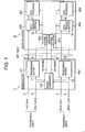
- a transmission system includes a sending system and a receiving system 2, which are connected by a single cable 301.
- the sending system 1 receives a plurality of pairs of data and clock signals, which are not synchronized to each other.
- the sending system 1 includes a transmission section 101, a transmission section 102, and a phase comparator 103.
- the sending system 1 receives a first pair of a data signal 3 and a clock signal 4 through a first transmission line and a second pair of a data signal 5 and a clock signal 6 through a second transmission line.
- the transmission sections 101 and 102 receive the input data signals 3 and 4 and clock signals 11 and 12 that are received from the phase comparator 103, and transmits a pair of a data signal 7 and a clock signal 8 corresponding to the first pair and a pair of a data signal 9 and a clock signal 10 corresponding to the second pair.
- the phase comparator 103 compares the clock signals 4 and 6 to produce monostable trigger signals 13 and 14, each indicating possible crosstalk timings, at which crosstalk may be generated at the receiving system 2. More specifically, the trigger signal 13 indicates the timing of possible crosstalk from the data signal 9 to the data signal 7 and the trigger signal 14 indicates the timing of possible crosstalk from the data signal 7 to the data signal 9. The details of the phase comparator 103 will be described later.
- the sending system 1 transmits a pair of the data signal 7 and the clock signal 8, a pair of the data signal 9 and the clock signal 10, and the trigger signals 13 and 14 to the receiving system 2 through the cable 301.
- the clock signals 4 and 6 are not synchronized and both clock frequencies are low.
- the clock signals 8 and 10 are also not synchronized and both clock frequencies are low.
- the receiving system 2 includes data processors 201 and 202, phase shifters 203 and 204, and data reading sections 205 and 206.
- the phase shifter 203 receives the clock signal 8 and the trigger signal 13 indicating the timing of possible crosstalk from the data signal 9 to the data signal 7. Then the trigger signal 13 is output, the phase shifter 203 shifts the phase of the clock signal 8 to the timing at which no crosstalk could be generated to produce a reading clock signal 15. As described later, the amount of the time shift is determined depending on the pulse width of the trigger signal 13. When the trigger signal 13 is not output, the phase shifter 203 outputs the clock signal 8 as the reading clock signal 15.
- the data reading section 205 reads a first data signal from the data signal 7 according to the reading clock signal 15 having the timing at which no crosstalk could be generated. Thereafter, the data reading section 205 further reads a second data signal 17 from the first data signal according to the clock signal 8 for synchronization with the clock signal 8.
- the phase shifter 204 receives the clock signal 10 and the trigger signal 14 indicating the timing of possible crosstalk from the data signal 7 to the data signal 9.
- the phase shifter 204 shifts the phase of the clock signal 10 to the timing at which no crosstalk could be generated to produce a reading clock signal 16.
- the amount of the time shift is determined depending on the pulse width of the trigger signal 14.
- the phase shifter 204 outputs the clock signal 10 as the reading clock signal 16.
- the data reading section 206 reads a first data signal from the data signal 9 according to the reading clock signal 16 having the timing at which no crosstalk could be generated. Thereafter, the data reading section 206 further reads a second data signal 18 from the first data signal according to the clock signal 10 for synchronization with the clock signal 10.
- the respective data processors 201 and 202 process the data signals 17 and 18 output from the data reading sections 205 and 206.
- the phase comparator 103 is provided with a trailing edge detector 104 and a leading edge detector 105, which detect the trailing edges and the leading edges of the clock signal 4, respectively, and a trailing edge detector 106 and a leading edge detector 107, which detect the trailing edges and the leading edges of the clock signal 6, respectively.
- the trailing edge timing of the clock signal 4 detected by the trailing edge detector 104 and the leading edge timing of the clock signal 6 detected by the leading edge detector 107 are output to a crosstalk timing detector 108.
- the trailing edge timing of the clock signal 6 detected by the trailing edge detector 106 and the leading edge timing of the clock signal 4 detected by the leading edge detector 105 are output to a crosstalk timing detector 109.
- a data signal changes in synchronization with the trailing edge timing of its clock signal. Therefore, when one of the clock signals 4 and 6 goes low before and after the other goes high, crosstalk is likely to occur.
- the crosstalk timing detector 108 detects a possible crosstalk timing in the data signal 7 to produce the trigger signal 13.
- the crosstalk timing detector 109 detects a possible crosstalk timing in the data signal 9 to produce the trigger signal 14.
- each of the trailing edge detectors 104 and 106 and the leading edge detectors 105 and 107 includes a delay circuit for delaying the corresponding input clock signal by a predetermined amount. Therefore, the clock signal 4 is delayed by a delay circuit 110 and the delayed clock signal 11 is output to the transmission section 101. Similarly, the clock signal 6 is delayed by a delay circuit 111 and the delayed clock signal 12 is output to the transmission section 102. Therefore, the delayed clock signals 11 and 12 are transmitted as the clock signals 8 and 10 through the cable 301, respectively.
- the crosstalk timing detector 108 of the phase comparator 103 detects possible crosstalk timing from the trailing edge timing 19 of the clock signal 4 detected by the trailing edge detector 104 and the leading edge timing 22 of the clock signal 6 detected by the leading edge detector 107.
- the crosstalk timing detector 108 outputs the trigger signal 13 having a pulse width(t1-t3) having the trailing edge timing t2 of the clock signal 8 located therein.
- the phase shifter 203 receives the clock signal 8 and the trigger signal 13. If the trigger signal 13 is in a logic level of "0", then the received clock signal 8 is supplied as a reading clock signal 15 to the data reading section 205 because no crosstalk occurs. If the trigger signal 13 is in a logic level of "1", which means that crosstalk may occur, then the phase shifter 203 shifts the trailing edge of the clock signal 8 to the trailing edge timing of the trigger signal 13 to produce a reading clock signal 15 as shown in (c) through (e) of Fig. 3. The trailing edge timing of the trigger signal 13 is located before the corresponding data signal changes. Therefore, the reading clock signal 15 produced by the phase shifter 203 always has the read timing at which no crosstalk occurs.
- the data reading section 205 reads a first data signal indicated by reference symbol "A" from the data signal 7 according to the timing of the reading clock signal 15 as shown at (h) of Fig. 3. Thereafter, the data reading section 205 further reads a second data signal 17 from the first data signal A according to the original timing of the clock signal 8 for synchronization with the clock signal 6 as shown in (i) of Fig. 3.
- the crosstalk timing detector 109 of the phase comparator 103 detects possible crosstalk timing from the trailing edge timing 21 of the clock signal 6 detected by the trailing edge detector 106 and the leading edge timing 20 of the clock signal 4 detected by the leading edge detector 105.
- the crosstalk timing detector 109 outputs the trigger signal 14 having a pulse width (t5-t7) having the trailing edge timing t6 of the clock signal 10 located therein.
- the phase shifter 204 receives the clock signal 10 and the trigger signal 14. If the trigger signal 14 is at a logic level of "0". then the received clock signal 10 is supplied as a reading clock signal 16 to the data reading section 206, because no crosstalk occurs. If the trigger signal 14 is at a logic level of "1", which means that crosstalk may occur, then the phase shifter 204 shifts the trailing edge of the clock signal 10 to the trailing edge timing of the trigger signal 14 to produce a reading clock signal 16 as shown in (c) through (e) of Fig. 4. The trailing edge timing of the trigger signal 14 is located before the corresponding data signal changes. Therefore, the reading clock signal 16 produced by the phase shifter 204 always has the timing at which no crosstalk occurs.
- the data reading section 206 reads a first data signal indicated by reference symbol "B" from the data signal 9 according to the timing of the reading clock signal 16 as shown at (h) of Fig. 4. Thereafter, the data reading section 206 further reads a second data signal 18 from the first data signal B according to the original timing of the clock signal 10 for synchronization with the clock signal 10 as shown in (i) of Fig. 4.
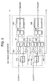
- phase comparator 103 An example of the phase comparator 103 will be described with reference to Figs. 5 and 6.
- the phase comparator 103 as described with reference to Fig. 2, is provided with the trailing edge detector 104 and the leading edge detector 105, the trailing edge detector P106, the leading edge detector 107, and the delay circuits 110 and 111.
- the trailing edge detector 104 includes an inverter and an AND gate that performs a logical AND operation on the delayed clock signal 11 and a clock signal obtained by the inverter, logically inverting the clock signal 4 to produce the trailing edge timing signal 19 of the clock signal 4.
- the leading edge detector 105 includes an inverter and an AND gate that performs a logical AND operation on the clock signal 4, and a clock signal obtained by the inverter inverting the delayed clock signal 11 to produce the leading edge timing signal 20 of the clock signal 4.
- the trailing edge detector 106 includes an inverter and an AND gate that performs a logical AND operation on the delayed clock signal 12 and a clock signal obtained by the inverter, logically inverting the clock signal 6 to produce the trailing edge timing signal 21 of the clock signal 6.
- the leading edge detector 107 includes an inverter and an AND gate that performs a logical AND operation on the clock signal 6 and a clock signal obtained by the inverter, inverting the delayed clock signal 12 to produce the leading edge timing signal 22 of the clock signal 6.
- the crosstalk timing detector 106 includes an AND gate and an integrator.
- the AND gate performs a logical AND operation on the trailing edge timing signal 19 and the leading edge timing signal 22 to produce an AND output signal 23.
- the integrator performs the integration of the AND output signal 23 to produce the trigger signal 13 having a sufficient pulse width.
- the crosstalk timing detector 109 includes an AND gate and an integrator.
- the AND gate performs a logical AND operation on the trailing edge timing signal 21 and the leading edge timing signal 20 to produce an AND output signal 24.
- the integrator performs the integration of the AND output signal 24 to produce the trigger signal 14 having a sufficient pulse width.
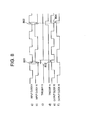
- a data signal 3 changes in synchronization with the trailing edge timing of its clock signal 4. Therefore, when the clock signal 4 goes low (L) Just after the clock signal 6 goes high (H). as indicated by reference numeral 601, crosstalk from the data signal 9 to the data signal 7 is likely to occur.
- the crosstalk timing detector 108 detects a possible crosstalk timing (AND output 23) in the data signal 7 to produce the trigger signal 13, which has been widened by the integrator 105 to cover the possible crosstalk timing.
- the crosstalk timing detector 109 detects a possible crosstalk timing (AND output 24) in the data signal 9 to produce the trigger signal 14, which has been widened by the integrator 108 to cover the possible crosstalk timing.
- the phase shifter 203 receives the clock signal 8 and the trigger signal 13 indicating the timing of possible crosstalk from the data signal 9 to the data signal 7 Similarly, the phase shifter 204 receives the clock signal 10 and the trigger signal 14 indicating the timing of possible crosstalk from the data signal 7 to the data signal 9.
- each of the phase shifters 203 and 204 includes a selector, which selects one of inputs A and B depending on a selection signal S and outputs a selected one as a reading clock signal.
- the selector of the phase shifter 203 inputs the clock signal 8 as input A, a fixed signal being a logic state of 3. (high) as input B and the trigger signal 13 as the selection signal S.
- the selector selects the clock signal 8 to output it as the reading clock signal 15.
- the selector selects the fixed signal being a logic state of 1 (high) to output it as the reading clock signal 15.
- the selector of the phase shifter 204 inputs the clock signal 10 as input A, a fixed signal being a logic state of 1 (high) as input B and the trigger signal 14 as the selection signal S.
- the selector selects the clock signal 10 to output it as the reading clock signal 16.
- the selector selects the fixed signal, being in a logic state of 1. (high) to output it as the reading clock signal 16.
- the crosstalk timing detector 108 produces the trigger signal 13 having a pulse width during which the possible crosstalk timing 801 is included and outputs it to the receiving system 2 as shown in (c) of Fig. 8.
- the phase shifter 203 receives the clock signal B and the trigger signal 13 from the sending system 1. If the trigger signal 13 is at a low level "0", then the phase shifter 203 selects the received clock signal 8 as a reading clock signal 15 to the data reading section 205 because no crosstalk occurs. However, if the trigger signal 13 is at a high level "1", then the phase shifter 203 selects the fixed signal being the logic state of High to shift the trailing edge of the clock signal 8 to the trailing edge timing of the trigger signal 13 to produce the reading clock signal 15 as shown at (e) in Fig. 8. Therefore, the reading clock signal 16 produced by the phase shifter 204 always has the reading timing at which no crosstalk occurs. It is the same with the phase shifter 204.
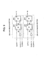
- the data reading section 205 includes a first flip-flop circuit 901 and a second flip-flop circuit 902.
- the first flip-flop circuit 901 inputs the data signal 7 at the input D and a clock signal 25 generated by an inverter inverting the reading clock signal 15.
- the second flip-flop circuit 902 inputs the output 27 of the first flip-flop circuit 901 and the clock signal 8.
- the data reading section 206 includes a first flip-flop circuit 903 and a second flip-flop circuit 904.
- the first flip-flop circuit 903 Inputs the data signal 9 at the input D and a clock signal 26 generated by an inverter inverts the reading clock signal 16.
- the second flip-flop circuit 904 inputs the output 28 of the first flip-flop circuit 903 and the clock signal 10.
- the first flip-flop circuit 901 of the data reading section 205 reads a first data signal 27 from the data signal 7 according to the reading clock signal 15. More specifically, even if a crosstalk noise 1001 is generated by the data signal 9, the reading clock signal 15 has the trailing edge timing 1002 at which no crosstalk could be generated. Therefore, the first data signal 27 has no crosstalk noise. However, the first data signal 27 is not synchronized with the original clock signal 8.
- the second flip-flop circuit 902 further reads a second data signal 17 from the first data signal 27 according to the clock signal 8 for synchronization with the clock signal 8. In this way, the data signal 17 having no error can be output to the data processor 201.
- the first flip-flop circuit 903 of the data reading section 206 reads a first data signal 28 from the data signal 9 according to the reading clock signal 16. More specifically, even if a crosstalk noise 1003 is generated by the data signal 7, the reading clock signal 16 has the trailing edge timing 1004 at which no crosstalk could be generated. Therefore, the first data signal 25 has no crosstalk noise. However, the first data signal 28 is not synchronized with the original clock signal 10.
- the second flip-flop circuit 904 further reads a second data signal 18 from the first data signal 28 according to the clock signal 10 for synchronization with the clock signal 10. In this way, the data signal 18 having no error can be output to the data processor 202.
Landscapes
- Engineering & Computer Science (AREA)
- Computer Networks & Wireless Communication (AREA)
- Signal Processing (AREA)
- Synchronisation In Digital Transmission Systems (AREA)
- Dc Digital Transmission (AREA)
Claims (11)
- System zur Beseitigung von Übersprechen zwischen mehreren Datensignalen (7, 9), die durch ein Übertragungskabel (301) von einer Sendeeinrichtung (1) zu einer Empfangseinrichtung (2) laufen, wobei jeweils zu den Datensignalen gehörige Taktsignale (8, 10) nicht miteinander synchronisiert sind, dadurch gekennzeichnet, daß
die Sendeeinrichtung aufweist:eine Erkennungseinrichtung (103) zum Erkennen eines möglichen Übersprech-Zeitverlaufs in jedem der Datensignale durch Vergleichen von Phasen der Taktsignale, um den möglichen Übersprech-Zeitverlauf an die Empfangseinrichtung zu übertragen, unddie Empfangseinrichtung aufweist:eine Lesezeitverlauf-Verschiebungseinrichtung (203, 204) zum Verschieben eines Lesezeitverlaufs jedes der zu einem entsprechenden Datensignal gehörenden Taktsignale auf einen Zeitverlauf ohne Übersprechen, welcher auf der Grundlage des von der Sendeinrichtung empfangenen möglichen Übersprech-Zeitverlaufs bestimmt wird. - System nach Anspruch 1, wobei die Erkennungseinrichtung aufweist:wobei jede der Übersprech-Zeitverlauf-Erkennungseinrichtungen den möglichen Übersprech-Zeitverlauf in einem entsprechenden Datensignal auf der Grundlage des Abfallflanken-zeitverlaufs des entsprechenden zu ihm gehörenden Taktsignals und der Anstiegsflanken-Zeitverläufe aller anderen Taktsignale außer dem entsprechenden Taktsignal erkennt.mehrere Anstiegsflanken-Erkennungseinrichtungen (105, 107), die jeweiligen der Taktsignale entsprechen, wobei jede der Anstiegsflanken-Erkennungseinrichtungen einen Anstiegsflanken-Zeitverlauf eines entsprechenden Taktsignals erkennt;mehrere Abfallflanken-Erkennungseinrichtungen (104, 106), die jeweiligen der Taktsignale entsprechen, wobei jede der Abfallflanken-Erkennungseinrichtungen einen Abfallflanken-Zeitverlauf eines entsprechenden Taktsignals erkennt; undmehrere Übersprech-Zeitverlauf-Erkennungseinrichtungen (108, 109), die jeweiligen der Taktsignale entsprechen,
- System nach Anspruch 1, wobei die Empfangseinrichtung ferner aufweist:einen ersten Datenleseabschnitt (205) zum Lesen jedes der von der Sendeinrichtung empfangenen Datensignale gemäß des Zeitverlaufs ohne Übersprechen, um ein erstes Datensignal zu erzeugen; undeinen zweiten Datenleseabschnitt (206) zum Lesen des ersten Datensignals gemäß des Lesezeitverlaufs eines entsprechenden Taktsignals.
- System nach Anspruch 1, wobei
die Erkennungseinrichtung einen Phasenvergleicher zum Vergleichen von Phasen der Taktsignale aufweist, um mehrere Phasenverschiebungs-Auslösesignale (13, 14) zu erzeugen, welche mögliche Übersprech-Zeitverläufe für jeweilige der Datensignale anzeigen, um die Phasenverschiebungs-Auslösesignale an die Empfangseinrichtung zu übertragen;
wobei die Lesezeitverlauf-Verschiebungseinrichtung mehrere Lesezeitverlauf-Verschiebungsabschnitte aufweist, die jeweiligen der Phasenverschiebungs-Auslösesignale entsprechen, wobei jeder der Lesezeitverlaufabschnitte ein entsprechendes Phasenverschiebungs-Auslösesignal und ein entsprechendes Taktsignal empfängt und einen Lesezeitverlauf des entsprechenden Taktsignals (8, 10) abhängig von dem entsprechenden Phasenverschiebungs-Auslösesignal verschiebt, um ein entsprechendes verschobenes Lesezeitverlaufssignal zu erzeugen, und
die Empfangseinrichtung ferner mehrere Datenleseabschnitte (205, 206) aufweist, die entsprechenden der Lesezeitverlauf-Verschiebungseinrichtungen (203, 204) entsprechen, wobei jeder der Datenleseabschnitte ein entsprechendes Datensignal, das entsprechende Taktsignal und das entsprechende verschobene Lesezeitverlaufssignal empfängt und das entsprechende Datensignal entsprechend des Verschiebungseinrichtungs-Lesezeitverlaufssignals liest, um ein erstes Datensignal zu erzeugen und danach das erste Datensignal gemäß des entsprechenden Taktsignals zu lesen, um ein endgültiges Datensignal zu erzeugen. - System nach Anspruch 4, wobei der Phasenvergleicher aufweist:wobei jede der Übersprech-Zeitverlauf-Erkennungseinrichtungen den möglichen Übersprech-Zeitverlauf in einem entsprechenden Datensignal auf der Grundlage des Abfallflanken-Zeitverlaufs des entsprechenden zu ihm gehörenden Taktsignals und den Anstiegsflanken-Zeitverläufen aller anderen Taktsignale außer dem entsprechenden Taktsignal erkennt; undmehrere Anstiegsflanken-Erkennungseinrichtungen (105, 107), die jeweiligen der Taktsignale entsprechen, wobei jede der Anstiegsflanken-Erkennungseinrichtungen einen Anstiegsflanken-Zeitverlauf eines entsprechenden Taktsignals erkennt;mehrere Abfallflanken-Erkennungseinrichtungen (104, 106), die jeweiligen der Taktsignale entsprechen, wobei jede der Abfallflanken-Erkennungseinrichtungen einen Abfallflanken-Zeitverlauf eines entsprechenden Taktsignals erkennt;mehrere Übersprech-Zeitverlauf-Erkennungseinrichtungen (108, 109), die jeweiligen der Taktsignale entsprechen,
mehrere Triggerquellen, die jeweiligen der Phasenverschiebungss-Auslösesignale entsprechen, wobei jede der Triggerquellen das entsprechende Phasenverschiebungs-Auslösesignal aus dem entsprechenden möglichen Übersprech-Zeitverlauf erzeugt, wobei das entsprechende Phasenverschiebungs-Auslösesignal eine Impulsbreite hat, in der sich der entsprechende mögliche Übersprech-Zeitverlauf befindet. - System nach Anspruch 4, wobei jeder der Lesezeitverlaufsabschnitte eine Wahlvorrichtung zum Auswählen des entsprechenden Taktsignals oder eines festen Signals auf einem logischen Hochpegel abhängig von dem entsprechenden Phasenverschiebungs-Auslösesignal aufweist, wobei das entsprechende Taktsignal ausgewählt wird, wenn das entsprechende Phasenverschiebungs-Auslösesignal einen logischen Tiefpegel hat, und das feste Signal ausgewählt wird, wenn das entsprechende Phasenverschiebungs-Auslösesignal einen logischen Hochpegel hat.
- System nach Anspruch 6, wobei jeder der Datenlesesabschnitte (205, 206) aufweist:eine erste Flip-Flop-Schaltung (901, 903) zum Lesen des entsprechenden Datensignals gemäß des entsprechenden verschobenen Lesezeitverlaufssignals, um das erste Datensignal (27, 28) zu erzeugen; undeine zweite Flip-Flop-Schaltung (902, 904) zum Lesen des ersten Datensignals gemäß des entsprechenden Taktsignals.
- Verfahren zur Beseitigung von Übersprechen zwischen mehreren Datensignalen die durch ein Übertragungskabel von einer Sendeeinrichtung zu einer Empfangseinrichtung laufen, wobei jeweils zu den Datensignalen gehörige Taktsignale nicht miteinander synchronisiert sind, gekennzeichnet durch die folgenden Schritte:in der Sendeeinrichtung:a) Erkennen eines möglichen Übersprech-Zeitverlaufs in jedem der Datensignale durch Vergleichen von Phasen der Taktsignale, um den möglichen Übersprech-Zeitverlauf an die Empfangseinrichtung zu übertragen; undin der Empfangseinrichtung:b) Verschieben eines Lesezeitverlaufs jedes der zu einem entsprechenden Datensignal gehörenden Taktsignale auf einen Zeitverlauf ohne Übersprechen, welcher auf der Grundlage des von der Sendeinrichtung empfangenen möglichen Übersprech-Zeitverlaufs bestimmt wird.
- Verfahren nach Anspruch 8, wobei der schritt (a) die folgenden Schritte aufweist:Erkennen eines Anstiegsflanken-Zeitverlaufs jedes der Taktsignale;Erkennen eines Abfallflanken-Zeitverlaufs des Taktsignals; undErkennen des möglichen Übersprech-Zeitverlaufs in einem entsprechenden Datensignal auf der Grundlage des Abfallflanken-Zeitverlaufs des zu ihm gehörenden Taktsignals und der Anstiegsflanken-Zeitverläufe aller anderen Taktsignale außer dem Taktsignal.
- Verfahren nach Anspruch 8, das ferner die folgenden Schritte aufweist:in der Empfangseinrichtung:c) Lesen jedes der von der Sendeinrichtung empfangenen Datensignale gemäß des Zeitverlaufs ohne Übersprechen, um ein erstes Datensignal zu erzeugen; undd) Lesen des ersten Datensignals gemäß des Lesezeitverlaufs eines entsprechenden Taktsignals.
- Verfahren nach Anspruch 8, wobei der Schritt a) einen Schritt zum Vergleichen von Phasen der Taktsignale aufweist, um ein Phasenverschiebungs-Auslösesignal zu erzeugen, welches einen mögliche Übersprech-Zeitverlauf für jedes der Datensignale anzeigt, um das Phasenverschiebungs-Auslösesignal an die Empfangseinrichtung zu übertragen;
wobei der Schritt b) den folgenden Schritt aufweist:wobei das Verfahren ferner die folgenden Schritte aufweist:Empfangen des Phasenverschiebungs-Auslösesignals und eines entsprechenden Taktsignals; undVerschieben eines Lesezeitverlaufs des entsprechenden Taktsignals abhängig von dem Phasenverschiebungs-Auslösesignal, um ein verschobenes Lesezeitverlaufssignal zu erzeugen,in der Empfangseinrichtung:c) Lesen des Datensignals entsprechend des Verschiebungseinrichtungs-Lesezeitverlaufssignals, um ein erstes Datensignal zu erzeugen; undd) Lesen des ersten Datensignals gemäß des entsprechenden Taktsignals, um ein endgültiges Datensignal zu erzeugen.
Applications Claiming Priority (2)
| Application Number | Priority Date | Filing Date | Title |
|---|---|---|---|
| JP23502899A JP3645751B2 (ja) | 1999-08-23 | 1999-08-23 | 伝送システム |
| JP23502899 | 1999-08-23 |
Publications (3)
| Publication Number | Publication Date |
|---|---|
| EP1085672A2 EP1085672A2 (de) | 2001-03-21 |
| EP1085672A3 EP1085672A3 (de) | 2001-11-21 |
| EP1085672B1 true EP1085672B1 (de) | 2005-12-14 |
Family
ID=16980020
Family Applications (1)
| Application Number | Title | Priority Date | Filing Date |
|---|---|---|---|
| EP00307257A Expired - Lifetime EP1085672B1 (de) | 1999-08-23 | 2000-08-23 | Verfahren und System zur Minimierung von Übersprechen |
Country Status (4)
| Country | Link |
|---|---|
| US (1) | US6807236B1 (de) |
| EP (1) | EP1085672B1 (de) |
| JP (1) | JP3645751B2 (de) |
| CA (1) | CA2316514C (de) |
Families Citing this family (5)
| Publication number | Priority date | Publication date | Assignee | Title |
|---|---|---|---|---|
| US7142501B1 (en) * | 2001-12-26 | 2006-11-28 | Cisco Technology, Inc. | Method and apparatus for eliminating near-end crosstalk in a digital subscriber line system |
| US6975136B2 (en) * | 2003-03-20 | 2005-12-13 | Hewlett-Packard Development Company, L.P. | Isolated channel in an integrated circuit |
| DE60319703T2 (de) * | 2003-09-30 | 2009-03-19 | Qimonda Ag | Gerät und Verfahren zum Reduzieren von Übersprechen zwischen Übertragungssignalen |
| JP2015046715A (ja) * | 2013-08-27 | 2015-03-12 | 富士通株式会社 | 通信回路及び情報処理装置 |
| WO2018012819A1 (ko) * | 2016-07-13 | 2018-01-18 | 주식회사 케이티 | 번들 케이블 내 이종 기술간 공존 간섭을 회피하는 방법 및 장치 |
Family Cites Families (8)
| Publication number | Priority date | Publication date | Assignee | Title |
|---|---|---|---|---|
| US4281409A (en) * | 1979-06-25 | 1981-07-28 | Schneider Kenneth S | Method and apparatus for multiplex binary data communication |
| DE4032067A1 (de) * | 1990-10-10 | 1992-04-16 | Standard Elektrik Lorenz Ag | Leitungseinrichtung zur kompensation von nebensprechen |
| JPH1041981A (ja) * | 1996-07-19 | 1998-02-13 | Hitachi Ltd | ベースバンド信号送受信方法 |
| US5887032A (en) * | 1996-09-03 | 1999-03-23 | Amati Communications Corp. | Method and apparatus for crosstalk cancellation |
| US6144242A (en) * | 1997-09-04 | 2000-11-07 | Silicon Image, Inc. | Controllable delays in multiple synchronized signals for reduced electromagnetic interference at peak frequencies |
| US6307906B1 (en) * | 1997-10-07 | 2001-10-23 | Applied Micro Circuits Corporation | Clock and data recovery scheme for multi-channel data communications receivers |
| ATE297623T1 (de) * | 1998-10-30 | 2005-06-15 | Broadcom Corp | Internet-gigabit-ethernet-sender-architektur |
| US6385252B1 (en) * | 1999-05-28 | 2002-05-07 | Lucent Technologies Inc. | High density multiple digital signal connection interface with reduced cross talk |
-
1999
- 1999-08-23 JP JP23502899A patent/JP3645751B2/ja not_active Expired - Fee Related
-
2000
- 2000-08-22 CA CA002316514A patent/CA2316514C/en not_active Expired - Fee Related
- 2000-08-23 EP EP00307257A patent/EP1085672B1/de not_active Expired - Lifetime
- 2000-08-23 US US09/644,043 patent/US6807236B1/en not_active Expired - Fee Related
Also Published As
| Publication number | Publication date |
|---|---|
| EP1085672A3 (de) | 2001-11-21 |
| CA2316514C (en) | 2003-08-19 |
| JP2001060977A (ja) | 2001-03-06 |
| EP1085672A2 (de) | 2001-03-21 |
| US6807236B1 (en) | 2004-10-19 |
| JP3645751B2 (ja) | 2005-05-11 |
| CA2316514A1 (en) | 2001-02-23 |
Similar Documents
| Publication | Publication Date | Title |
|---|---|---|
| US6567484B1 (en) | Burst synchronizing circuit | |
| US7254201B2 (en) | Clock and data recovery circuit and method | |
| EP1085672B1 (de) | Verfahren und System zur Minimierung von Übersprechen | |
| EP0833478B1 (de) | Vorrichtung zur Musterwiedererkennung | |
| JP2947074B2 (ja) | フレーム同期検出回路 | |
| EP0257301B1 (de) | PSK-System und -Modem | |
| US4213007A (en) | Method and apparatus for monitoring a pulse-code modulated data transmission | |
| US5206887A (en) | Unique word detection apparatus | |
| EP0094058B1 (de) | Demodulatoranordnung für mit zusammengesetzter Phasenumtastung modulierten Wellen | |
| CN113923090B (zh) | 移动设备网络的帧同步检测方法、系统和计算机存储介质 | |
| JPH06120995A (ja) | ディジタル無線用受信機のフレーム同期回路 | |
| US7161986B2 (en) | Data transmission system and data transmitter/receiver for use therein, and method thereof | |
| JPH11340839A (ja) | パラレル信号シリアル伝送装置 | |
| EP1209912A1 (de) | Daten-Slicer-Schaltung | |
| JPH10145350A (ja) | インターコネクション回路 | |
| JPS60141057A (ja) | 変復調切換え方式 | |
| JP3082337B2 (ja) | スペースダイバーシティ同相合成回路 | |
| SU853802A2 (ru) | Адаптивное устройство синхрони-зАции гЕНЕРАТОРОВ СЕТи СВ зи | |
| JPS6365251B2 (de) | ||
| JP2616450B2 (ja) | クロック供給システム | |
| JP3429620B2 (ja) | ワイドクリアビジョン受像機用デコーダ | |
| JPH06152669A (ja) | クロック再生回路 | |
| JPS62181556A (ja) | デイジタル変復調回路 | |
| JPH03255743A (ja) | ビット同期回路 | |
| JPH1056446A (ja) | バースト同期回路に於ける位相選択方法 |
Legal Events
| Date | Code | Title | Description |
|---|---|---|---|
| PUAI | Public reference made under article 153(3) epc to a published international application that has entered the european phase |
Free format text: ORIGINAL CODE: 0009012 |
|
| AK | Designated contracting states |
Kind code of ref document: A2 Designated state(s): FR GB Kind code of ref document: A2 Designated state(s): AT BE CH CY DE DK ES FI FR GB GR IE IT LI LU MC NL PT SE |
|
| AX | Request for extension of the european patent |
Free format text: AL;LT;LV;MK;RO;SI |
|
| PUAL | Search report despatched |
Free format text: ORIGINAL CODE: 0009013 |
|
| AK | Designated contracting states |
Kind code of ref document: A3 Designated state(s): AT BE CH CY DE DK ES FI FR GB GR IE IT LI LU MC NL PT SE |
|
| AX | Request for extension of the european patent |
Free format text: AL;LT;LV;MK;RO;SI |
|
| 17P | Request for examination filed |
Effective date: 20011024 |
|
| AKX | Designation fees paid |
Free format text: FR GB |
|
| REG | Reference to a national code |
Ref country code: DE Ref legal event code: 8566 |
|
| 17Q | First examination report despatched |
Effective date: 20040318 |
|
| GRAP | Despatch of communication of intention to grant a patent |
Free format text: ORIGINAL CODE: EPIDOSNIGR1 |
|
| GRAS | Grant fee paid |
Free format text: ORIGINAL CODE: EPIDOSNIGR3 |
|
| GRAA | (expected) grant |
Free format text: ORIGINAL CODE: 0009210 |
|
| AK | Designated contracting states |
Kind code of ref document: B1 Designated state(s): FR GB |
|
| REG | Reference to a national code |
Ref country code: GB Ref legal event code: FG4D |
|
| ET | Fr: translation filed | ||
| PLBE | No opposition filed within time limit |
Free format text: ORIGINAL CODE: 0009261 |
|
| STAA | Information on the status of an ep patent application or granted ep patent |
Free format text: STATUS: NO OPPOSITION FILED WITHIN TIME LIMIT |
|
| 26N | No opposition filed |
Effective date: 20060915 |
|
| PGFP | Annual fee paid to national office [announced via postgrant information from national office to epo] |
Ref country code: FR Payment date: 20090814 Year of fee payment: 10 |
|
| PGFP | Annual fee paid to national office [announced via postgrant information from national office to epo] |
Ref country code: GB Payment date: 20090818 Year of fee payment: 10 |
|
| GBPC | Gb: european patent ceased through non-payment of renewal fee |
Effective date: 20100823 |
|
| REG | Reference to a national code |
Ref country code: FR Ref legal event code: ST Effective date: 20110502 |
|
| PG25 | Lapsed in a contracting state [announced via postgrant information from national office to epo] |
Ref country code: FR Free format text: LAPSE BECAUSE OF NON-PAYMENT OF DUE FEES Effective date: 20100831 |
|
| PG25 | Lapsed in a contracting state [announced via postgrant information from national office to epo] |
Ref country code: GB Free format text: LAPSE BECAUSE OF NON-PAYMENT OF DUE FEES Effective date: 20100823 |