EP1079362A2 - Elektrolumineszentes Anzeigegerät - Google Patents
Elektrolumineszentes Anzeigegerät Download PDFInfo
- Publication number
- EP1079362A2 EP1079362A2 EP00307101A EP00307101A EP1079362A2 EP 1079362 A2 EP1079362 A2 EP 1079362A2 EP 00307101 A EP00307101 A EP 00307101A EP 00307101 A EP00307101 A EP 00307101A EP 1079362 A2 EP1079362 A2 EP 1079362A2
- Authority
- EP
- European Patent Office
- Prior art keywords
- driving
- row
- period
- column
- display apparatus
- Prior art date
- Legal status (The legal status is an assumption and is not a legal conclusion. Google has not performed a legal analysis and makes no representation as to the accuracy of the status listed.)
- Withdrawn
Links
- 238000005401 electroluminescence Methods 0.000 title claims abstract description 24
- 239000000463 material Substances 0.000 claims description 33
- 239000003086 colorant Substances 0.000 claims description 26
- 238000000034 method Methods 0.000 claims description 8
- 101100328886 Caenorhabditis elegans col-2 gene Proteins 0.000 description 19
- 101100328884 Caenorhabditis elegans sqt-3 gene Proteins 0.000 description 15
- 238000012937 correction Methods 0.000 description 13
- 101100328883 Arabidopsis thaliana COL1 gene Proteins 0.000 description 7
- 238000012546 transfer Methods 0.000 description 7
- 101100328890 Arabidopsis thaliana COL3 gene Proteins 0.000 description 6
- 238000010586 diagram Methods 0.000 description 6
- 101100004188 Arabidopsis thaliana BARD1 gene Proteins 0.000 description 2
- 239000011159 matrix material Substances 0.000 description 2
- 238000012986 modification Methods 0.000 description 2
- 230000004048 modification Effects 0.000 description 2
- 239000000758 substrate Substances 0.000 description 2
- WBEDMFHOODHFKR-UHFFFAOYSA-N 1-n,1-n'-bis(3-methylphenyl)-1-n,1-n',4-triphenylcyclohexa-2,4-diene-1,1-diamine Chemical group CC1=CC=CC(N(C=2C=CC=CC=2)C2(C=CC(=CC2)C=2C=CC=CC=2)N(C=2C=CC=CC=2)C=2C=C(C)C=CC=2)=C1 WBEDMFHOODHFKR-UHFFFAOYSA-N 0.000 description 1
- NRCMAYZCPIVABH-UHFFFAOYSA-N Quinacridone Chemical compound N1C2=CC=CC=C2C(=O)C2=C1C=C1C(=O)C3=CC=CC=C3NC1=C2 NRCMAYZCPIVABH-UHFFFAOYSA-N 0.000 description 1
- 239000007983 Tris buffer Substances 0.000 description 1
- JHYLKGDXMUDNEO-UHFFFAOYSA-N [Mg].[In] Chemical compound [Mg].[In] JHYLKGDXMUDNEO-UHFFFAOYSA-N 0.000 description 1
- 239000000956 alloy Substances 0.000 description 1
- 229910045601 alloy Inorganic materials 0.000 description 1
- GQVWHWAWLPCBHB-UHFFFAOYSA-L beryllium;benzo[h]quinolin-10-olate Chemical compound [Be+2].C1=CC=NC2=C3C([O-])=CC=CC3=CC=C21.C1=CC=NC2=C3C([O-])=CC=CC3=CC=C21 GQVWHWAWLPCBHB-UHFFFAOYSA-L 0.000 description 1
- 238000009125 cardiac resynchronization therapy Methods 0.000 description 1
- 239000011521 glass Substances 0.000 description 1
- 230000005525 hole transport Effects 0.000 description 1
- 238000012827 research and development Methods 0.000 description 1
Images


Classifications
-
- G—PHYSICS
- G09—EDUCATION; CRYPTOGRAPHY; DISPLAY; ADVERTISING; SEALS
- G09G—ARRANGEMENTS OR CIRCUITS FOR CONTROL OF INDICATING DEVICES USING STATIC MEANS TO PRESENT VARIABLE INFORMATION
- G09G3/00—Control arrangements or circuits, of interest only in connection with visual indicators other than cathode-ray tubes
- G09G3/20—Control arrangements or circuits, of interest only in connection with visual indicators other than cathode-ray tubes for presentation of an assembly of a number of characters, e.g. a page, by composing the assembly by combination of individual elements arranged in a matrix no fixed position being assigned to or needed to be assigned to the individual characters or partial characters
- G09G3/22—Control arrangements or circuits, of interest only in connection with visual indicators other than cathode-ray tubes for presentation of an assembly of a number of characters, e.g. a page, by composing the assembly by combination of individual elements arranged in a matrix no fixed position being assigned to or needed to be assigned to the individual characters or partial characters using controlled light sources
- G09G3/30—Control arrangements or circuits, of interest only in connection with visual indicators other than cathode-ray tubes for presentation of an assembly of a number of characters, e.g. a page, by composing the assembly by combination of individual elements arranged in a matrix no fixed position being assigned to or needed to be assigned to the individual characters or partial characters using controlled light sources using electroluminescent panels
- G09G3/32—Control arrangements or circuits, of interest only in connection with visual indicators other than cathode-ray tubes for presentation of an assembly of a number of characters, e.g. a page, by composing the assembly by combination of individual elements arranged in a matrix no fixed position being assigned to or needed to be assigned to the individual characters or partial characters using controlled light sources using electroluminescent panels semiconductive, e.g. using light-emitting diodes [LED]
- G09G3/3208—Control arrangements or circuits, of interest only in connection with visual indicators other than cathode-ray tubes for presentation of an assembly of a number of characters, e.g. a page, by composing the assembly by combination of individual elements arranged in a matrix no fixed position being assigned to or needed to be assigned to the individual characters or partial characters using controlled light sources using electroluminescent panels semiconductive, e.g. using light-emitting diodes [LED] organic, e.g. using organic light-emitting diodes [OLED]
- G09G3/3216—Control arrangements or circuits, of interest only in connection with visual indicators other than cathode-ray tubes for presentation of an assembly of a number of characters, e.g. a page, by composing the assembly by combination of individual elements arranged in a matrix no fixed position being assigned to or needed to be assigned to the individual characters or partial characters using controlled light sources using electroluminescent panels semiconductive, e.g. using light-emitting diodes [LED] organic, e.g. using organic light-emitting diodes [OLED] using a passive matrix
-
- G—PHYSICS
- G09—EDUCATION; CRYPTOGRAPHY; DISPLAY; ADVERTISING; SEALS
- G09G—ARRANGEMENTS OR CIRCUITS FOR CONTROL OF INDICATING DEVICES USING STATIC MEANS TO PRESENT VARIABLE INFORMATION
- G09G3/00—Control arrangements or circuits, of interest only in connection with visual indicators other than cathode-ray tubes
- G09G3/20—Control arrangements or circuits, of interest only in connection with visual indicators other than cathode-ray tubes for presentation of an assembly of a number of characters, e.g. a page, by composing the assembly by combination of individual elements arranged in a matrix no fixed position being assigned to or needed to be assigned to the individual characters or partial characters
- G09G3/22—Control arrangements or circuits, of interest only in connection with visual indicators other than cathode-ray tubes for presentation of an assembly of a number of characters, e.g. a page, by composing the assembly by combination of individual elements arranged in a matrix no fixed position being assigned to or needed to be assigned to the individual characters or partial characters using controlled light sources
- G09G3/30—Control arrangements or circuits, of interest only in connection with visual indicators other than cathode-ray tubes for presentation of an assembly of a number of characters, e.g. a page, by composing the assembly by combination of individual elements arranged in a matrix no fixed position being assigned to or needed to be assigned to the individual characters or partial characters using controlled light sources using electroluminescent panels
- G09G3/32—Control arrangements or circuits, of interest only in connection with visual indicators other than cathode-ray tubes for presentation of an assembly of a number of characters, e.g. a page, by composing the assembly by combination of individual elements arranged in a matrix no fixed position being assigned to or needed to be assigned to the individual characters or partial characters using controlled light sources using electroluminescent panels semiconductive, e.g. using light-emitting diodes [LED]
- G09G3/3208—Control arrangements or circuits, of interest only in connection with visual indicators other than cathode-ray tubes for presentation of an assembly of a number of characters, e.g. a page, by composing the assembly by combination of individual elements arranged in a matrix no fixed position being assigned to or needed to be assigned to the individual characters or partial characters using controlled light sources using electroluminescent panels semiconductive, e.g. using light-emitting diodes [LED] organic, e.g. using organic light-emitting diodes [OLED]
- G09G3/3275—Details of drivers for data electrodes
-
- G—PHYSICS
- G09—EDUCATION; CRYPTOGRAPHY; DISPLAY; ADVERTISING; SEALS
- G09G—ARRANGEMENTS OR CIRCUITS FOR CONTROL OF INDICATING DEVICES USING STATIC MEANS TO PRESENT VARIABLE INFORMATION
- G09G2300/00—Aspects of the constitution of display devices
- G09G2300/04—Structural and physical details of display devices
- G09G2300/0439—Pixel structures
- G09G2300/0452—Details of colour pixel setup, e.g. pixel composed of a red, a blue and two green components
-
- G—PHYSICS
- G09—EDUCATION; CRYPTOGRAPHY; DISPLAY; ADVERTISING; SEALS
- G09G—ARRANGEMENTS OR CIRCUITS FOR CONTROL OF INDICATING DEVICES USING STATIC MEANS TO PRESENT VARIABLE INFORMATION
- G09G2320/00—Control of display operating conditions
- G09G2320/02—Improving the quality of display appearance
- G09G2320/0233—Improving the luminance or brightness uniformity across the screen
-
- G—PHYSICS
- G09—EDUCATION; CRYPTOGRAPHY; DISPLAY; ADVERTISING; SEALS
- G09G—ARRANGEMENTS OR CIRCUITS FOR CONTROL OF INDICATING DEVICES USING STATIC MEANS TO PRESENT VARIABLE INFORMATION
- G09G2320/00—Control of display operating conditions
- G09G2320/02—Improving the quality of display appearance
- G09G2320/0242—Compensation of deficiencies in the appearance of colours
-
- G—PHYSICS
- G09—EDUCATION; CRYPTOGRAPHY; DISPLAY; ADVERTISING; SEALS
- G09G—ARRANGEMENTS OR CIRCUITS FOR CONTROL OF INDICATING DEVICES USING STATIC MEANS TO PRESENT VARIABLE INFORMATION
- G09G2320/00—Control of display operating conditions
- G09G2320/02—Improving the quality of display appearance
- G09G2320/0285—Improving the quality of display appearance using tables for spatial correction of display data
-
- G—PHYSICS
- G09—EDUCATION; CRYPTOGRAPHY; DISPLAY; ADVERTISING; SEALS
- G09G—ARRANGEMENTS OR CIRCUITS FOR CONTROL OF INDICATING DEVICES USING STATIC MEANS TO PRESENT VARIABLE INFORMATION
- G09G2320/00—Control of display operating conditions
- G09G2320/06—Adjustment of display parameters
- G09G2320/0626—Adjustment of display parameters for control of overall brightness
Definitions
- the present invention relates to a driving method for a passive matrix electroluminescence display apparatus comprising organic electroluminescence elements.
- EL display apparatuses using EL elements have attracted attention as display apparatuses to replace CRTs and LCDs, and the research and development into EL display apparatuses have also advanced.
- Fig. 1 shows a cross-sectional structure of a display section of an ordinary organic EL display apparatus.
- each organic EL element provided at each display pixel section has a laminated structure on a transparent glass substrate 1 in a sequence of an anode 2 formed from a transparent electrode, such as ITO, a hole transport layer 3 formed from MTDATA (4,4-bis(3-methylphenylphenylamino)biphenyl) and TPD (4,4,4-tris(3methylphenylphenylamino)triphenylanine), an emitting layer 4 formed from Bebq 2 (bis(10-hydroxybenzo[h]quinolinato) beryllium complex) including a Quinacridone inductor, an electron transport layer 5 formed from Bebq 2 , and a cathode 6 formed from a magnesium indium (MgIn) alloy.
- a transparent electrode such as ITO
- MTDATA 4,4-bis(3-methylphenylphenylamino)biphenyl
- TPD 4,4,4-tris(3methylphenylphenylamino)triphenylanine
- holes injected from the anode and electrons injected from the cathode are recombined within the emitting layer to excite the organic molecules forming the emitting layer and generate excitons.
- excitons are radiated and deactivated
- light is released from the emitting layer. The light is then discharged to emit light to the outside from the transparent anode via the transparent insulating substrate.
- Fig. 2 shows a block diagram of a driving circuit of the organic EL display apparatus
- Fig. 3 shows a timing chart for driving the organic EL display apparatus.
- the organic EL display apparatus comprises a column driver 7, a row driver 8, and a display pixel section 12.
- Column electrodes col1, col2, col3, ..., colm which are arranged as stripes along the vertical direction of the columns in the same figure and which are the cathodes 6 of the organic EL elements connected to the column driver 7, and row electrodes row1, row2, row3, ..., rown, which are arranged as stripes along the horizontal direction of the rows and which are the anodes 2 of the organic EL elements connected to the row driver 8, intersect each other, and display pixels PX11, PX12, ..., PXnm at the respective intersections are arranged in a matrix configuration.
- a transfer clock CLK As shown in Figs. 1 and 2, to the column driver 7 are supplied a transfer clock CLK, transfer data DATA, and latch pulses LS for one line of data, and to the row driver 8 is supplied a row driver clock VCLK.
- Scanning signals are supplied in accordance with the row driver clock VCLK to the respective row electrodes row1, row2, row3, ..., rown, which are cathodes on one side of the organic EL display elements.
- the scanning signals become a low level at every horizontal scanning period in sequence from row electrode row1 so that the respective row electrode row1, row2, row3, ..., rown is selected.
- the transfer data DATA is supplied to the respective column electrodes col1, col2, col3, ..., colm, which are anodes on the other side, supplied the transfer data DATA by the latch pulses LS in accordance with the transfer clock CLK as transfer data, namely, driving signals.
- the respective display pixels PX11 to PXnm which are provided at the respective intersections of the respective row electrodes row1, row2, row3, ..., rown and the respective column electrodes col1, col2, col3, ..., colm, emit light in colors corresponding to the luminescent materials of various colors provided at the display pixel section.
- the display colors of the display pixels will be described for the case where display pixel PX12 furnishes a red color, display pixel PX23 furnishes a blue color, and the other display pixels PX11 to PX13, PX21, and PX31 to PX33 furnish a green color.
- a low level scanning signal ROW1 is supplied to row electrode row1, only row electrode row1 is selected for 1H.
- the transfer data DATA in accordance with the transfer clock CLK is written with the latch pulse LS to the respective column electrodes col1, col2, and col3.
- the driving signals COL1, COL2, and COL3 are supplied to the respective column electrodes col1, col2, and col3.
- the display pixels PX11 to PX13 that are connected to the row electrode row1, are all green so that each of the display pixels emits green light for the period of 1H.
- the scanning signal ROW2 that is supplied to the row electrode row2 becomes a low level in accordance with the row driver clock VCLK so that the row electrode row2 is selected for 1H.
- the driving signals COL1, COL2, and COL3 are supplied to the respective column electrodes col1, col2, and col3, and the luminescent material of the various colors provided at the display pixels PX21 to PX23 at the respective intersections emit light.
- display pixel PX21 emits green light
- display pixel PX22 emits red light
- display pixel PX23 emits blue light.
- the display pixels emit light only during the period when the row electrode is selected, namely, the period of 1H.
- the scanning signal ROW3 that is supplied becomes a low level in accordance with the row driver clock VCLK so that the row electrode row3 is selected for 1H
- the driving signals COL1, COL2, and COL3 are supplied to the respective column electrodes col1, col2, and col3 so that the luminescent materials provided at the display pixels PX31 to PX33 at the respective intersections emit light.
- the respective display pixels PX31 to PX33 emit light only during the period when the row electrode is selected, namely, the period of 1H.
- the respective row electrodes row1, row2, and row3 are each selected for a period of 1H. Namely, the respective display pixels PX11 to PX33 emit light in a color corresponding to the luminescent material of the respective color only for a period of 1H.
- the luminescent materials of the respective colors provided at the respective display pixels PX11 to PX33 have different luminous efficiencies that depend on the material.
- the display pixels of the various colors emit light for the same period, namely, for the period of 1H, there is a shortcoming where the luminance of the colors is not uniform.
- PWM pulse width modulation
- the column driver 7 comprises a shift register 13 for inputting n-bit gradation data mDATA for each column according to a shift clock CL, a latch circuit 14 for latching the data that was input to the shift register 13 in accordance with the latch pulse, an n-bit counter 15 for representing the gradation levels, and m number of pulse width modulation circuits 16 for comparing the n-bit gradation data from the latch circuit 14 provided for each column and the n-bit counter value, then respectively outputting the column driving signals COL1, COL2, COL3, ..., COLm having pulse widths proportional to the gradation data.
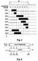
- the count value of the n-bit counter 15 changes in a sequence of "0", “1", ..., "7" during 1H as shown in Fig. 5, and the driving signals COL1, COL2, COL3, ..., COLm for the column electrodes all simultaneously begin output at a timing when the counter value becomes "1".
- the high level is maintained during the pulse width period in accordance with the gradation data for the respective pixel. Therefore, the display pixels in the same row emit light, and the light emitting period of each display pixel is controlled in accordance with the gradation data.
- the driving signal is supplied to each column electrode so as to cause the electroluminescence element of the corresponding display pixel to emit light when one row electrode has been selected by the selection signal.
- the driving period in which the driving signal is impressed so as to cause the corresponding display pixel to emit light is determined on the basis of the color of the display pixel that is to emit light.
- the driving period is shortened (such as to a length of "1") for the electroluminescence element for emitting green light, which has a high luminous efficiency, set to a medium length (such as to a length of "2") for the electroluminescence element for emitting red light, which has a medium luminous efficiency, and lengthened (such as to a length of "4") for the electroluminescence element for emitting blue light, which has a poor luminous efficiency.
- the brightness of the colors can be made equal using a simple configuration, without using pulse width modulation or the like.
- Fig. 1 is a cross-sectional view of an ordinary EL display apparatus.
- Fig. 2 is a block diagram of a driving circuit of the EL display apparatus.
- Fig. 3 is a timing chart for the EL display apparatus of the prior art.
- Fig. 4 is a block diagram of a column driver of the prior art.
- Fig. 5 is a timing chart of conventional pulses.
- Fig. 6 is a block diagram of a column driver of the present invention.
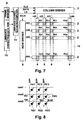
- Fig. 7 is a block diagram of a driving circuit representing an embodiment of the present invention.
- Fig. 8 an equivalent circuit of part of the EL display apparatus representing an embodiment of the present invention.
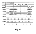
- Fig. 9 is a timing chart representing an embodiment of the present invention.
- a driving method for an EL display apparatus of the present invention is described hereinafter.
- Fig. 6 is a block diagram of a column driver.
- the column driver comprises the shift register 13 for inputting the data DATA for each column according to the shift clock CLK and the latch circuit 14 for latching in accordance with the latch pulse the data DATA that was input by the shift register 13.
- the driving signals COL1, COL2, COL3, ..., COLm are respectively output to the column electrodes col1, col2, col3, ..., colm from the latch circuit 14.
- the organic EL display apparatus of the present invention obviates the pulse width modulation circuits. Therefore, compared to the extreme complexity as in the column driver of the organic EL display apparatus of the prior art, the column driver of the organic EL display apparatus of the present invention can be designed to have an extremely simple configuration. Thus, it is possible to fabricate the column driver into an IC device.
- the organic EL display apparatus comprises the column driver 7 shown in Fig. 6, the row driver 8, and the display pixel section 12, and further comprises a frame memory 9, a luminance correction data ROM 10, and a luminance correction microcomputer 11.
- the data to be displayed on the organic EL display apparatus is stored from an external source into the frame memory 9.
- Information on the color and position arrangement on the organic EL display panel is stored beforehand in the luminance correction data ROM 10. Namely, in Fig. 8, for example, in the case where the display pixel PX21 is green and the display pixel PX22 is red, that information is stored into the luminance correction data ROM 10.
- the luminance correction control microcomputer 11 When performing luminance correction, the luminance correction control microcomputer 11 reads out the data stored in the frame memory 9 and the information in the luminance correction data ROM 10, and outputs picture data, namely, driving signals, to the column driver 7.
- Fig. 9 shows a timing chart for driving of the organic EL display apparatus, which is an embodiment of a driving method for the EL display apparatus of the present invention.
- Fig. 8 shows the display pixels PX11 to PX13, PX21 to PX23, and PX31 to PX33 configured from both the column electrodes col1 to col3 and the row electrodes row1, to row3.
- the display pixel PX22 provides a red color
- the display pixel PX23 provides a blue color
- the other display pixels PX11 to PX13, PX21, and PX31 to PX33 provide a green color.
- the row electrodes row1, row2, and row3 are selected in sequence by row from row1, to row3.
- the scanning signal only for the selected row becomes a low level during one horizontal scanning period (1H), and the scanning signals for the other rows become a high level.
- the row electrode row1 is selected when the signal ROW1 that is supplied to the row electrode row1, becomes a low level.
- the row electrode row2 becomes a low level at a timing when the row electrode row1, becomes a high level.
- a red pixel with a luminous efficiency ratio of 1/2 and a blue pixel with a luminous efficiency ratio of 1/4 both with respect to green are provided in the row electrode row2.
- the selection time for the row electrode row2 is lengthened for the amount the luminous efficiency is low. Namely, the blue color is selected for a period four times that of the green color, or a period of 4H.
- a driving signal is supplied only for a period of 1H to the column electrode col1 so that the display pixel PX21 emits green light.
- a driving signal is supplied for a period of 2H to the column electrode col2 so that the display pixel PX22 emits red light.
- the driving signals are supplied to the column electrodes col1, col2, and col3 so that the display pixels PX21, PX22, and PX23 respectively emit green, red, and blue light.
- the driving signals are supplied only to the column electrodes col2 and col3 so that the display pixels PX22 and PX23 respectively emit red and blue light.
- the driving signal is supplied only to the column electrode col3 so that only the display pixel PX23 emits blue light.
- the row electrode row2 is selected four consecutive times (4H), and during those four times, the green display pixel PX21 emits light for one time (1H), the red display pixel PX22 emits light for two times (2H), and the blue display pixel PX23 emits light for four times (4H).
- the luminance correction control microcomputer 11 reads out various types of information from the frame memory 9 and the luminance correction data ROM 10 in which is stored beforehand information that the display pixel PX22 has a red luminescent material with a luminous efficiency lower than that of the green luminescent material provided at the display pixel PX21, and corresponding to that information, the information with part (green color) of the image data deleted is transferred to the column driver so as to cause the red and blue lights to be emitted.
- the organic EL display apparatus yields a uniform display without irregularities.
- the present invention exemplifies a case where the luminous efficiencies of the luminescent materials for the colors of green, red, and blue have the ratio of 1:1/2:1/4.
- the present invention is not limited to this case.
- the period for selecting the row electrode that is connected to the display pixel provided with luminescent material having the lowest luminous efficiency may be lengthened, and the period for supplying the driving signal to the column electrode connected to that pixel may be set so as to be the longest for the display pixel of the luminescent material having the lowest luminous efficiency.
- the present embodiment showed a case where the luminescent materials of the display pixels were for green, red, and blue.
- the application concerned is not limited to this case.
- the present invention is also applicable to a case using luminescent materials for yellow and white to yield the same effect.
- an order of the luminescent efficiency is green, yellow, white, red, blue, however this order may be changed in accordance with luminescent materials.
- the number of colors is not limited to three and any number of colors may be used. For example, if two colors are selected, it is necessary to select the number of selection times for the row electrode and the number of times for supplying the driving signal to the column electrode in proportion to the ratio of the luminous efficiencies of their luminescent materials.
- the selection time for the row electrode may be fixed and only the driving signal for the column electrode may be varied according to color.
- row electrodes and column electrodes is not limited and can be set in accordance with such requirements as resolution and display area.
- the luminous efficiency ratios of the luminescent materials in the present invention need not necessarily be integer values. In the event a ratio is not an integer value, luminance correction can still be performed when compared to the prior art even if an approximate integer is selected.
- an EL display apparatus can be obtained with a uniform luminance of the display pixels provided with luminescent materials of various colors having different luminous efficiencies.
Landscapes
- Engineering & Computer Science (AREA)
- Physics & Mathematics (AREA)
- Computer Hardware Design (AREA)
- General Physics & Mathematics (AREA)
- Theoretical Computer Science (AREA)
- Electroluminescent Light Sources (AREA)
- Control Of Indicators Other Than Cathode Ray Tubes (AREA)
- Control Of El Displays (AREA)
Applications Claiming Priority (2)
| Application Number | Priority Date | Filing Date | Title |
|---|---|---|---|
| JP24019999 | 1999-08-26 | ||
| JP24019999A JP4780815B2 (ja) | 1999-08-26 | 1999-08-26 | エレクトロルミネッセンス表示装置の駆動方法 |
Publications (2)
| Publication Number | Publication Date |
|---|---|
| EP1079362A2 true EP1079362A2 (de) | 2001-02-28 |
| EP1079362A3 EP1079362A3 (de) | 2002-10-02 |
Family
ID=17055941
Family Applications (1)
| Application Number | Title | Priority Date | Filing Date |
|---|---|---|---|
| EP00307101A Withdrawn EP1079362A3 (de) | 1999-08-26 | 2000-08-18 | Elektrolumineszentes Anzeigegerät |
Country Status (5)
| Country | Link |
|---|---|
| US (1) | US7154456B1 (de) |
| EP (1) | EP1079362A3 (de) |
| JP (1) | JP4780815B2 (de) |
| KR (1) | KR100347505B1 (de) |
| TW (1) | TW508973B (de) |
Cited By (2)
| Publication number | Priority date | Publication date | Assignee | Title |
|---|---|---|---|---|
| EP2717249A1 (de) * | 2012-10-04 | 2014-04-09 | Panasonic Corporation | LED-Anzeige und Heizkocher damit |
| WO2019217070A1 (en) * | 2018-05-09 | 2019-11-14 | Apple Inc. | Local passive matrix display |
Families Citing this family (11)
| Publication number | Priority date | Publication date | Assignee | Title |
|---|---|---|---|---|
| JP3757899B2 (ja) * | 2002-05-07 | 2006-03-22 | 株式会社豊田自動織機 | 駆動用半導体装置及び表示装置ならびに輝度バランス調整方法 |
| KR100459135B1 (ko) * | 2002-08-17 | 2004-12-03 | 엘지전자 주식회사 | 유기 el 디스플레이 패널 및 구동방법 |
| AT501629B1 (de) * | 2005-04-05 | 2007-10-15 | Erber Ag | Herstellung von hochgradig isotopenmarkierten, sekundären, mikrobiellen stoffwechselprodukten sowie stoffwechselprodukte |
| US7872617B2 (en) * | 2005-10-12 | 2011-01-18 | Canon Kabushiki Kaisha | Display apparatus and method for driving the same |
| KR100761296B1 (ko) * | 2006-03-17 | 2007-09-27 | 엘지전자 주식회사 | 발광 소자 및 이를 구동하는 방법 |
| US20100045190A1 (en) * | 2008-08-20 | 2010-02-25 | White Electronic Designs Corporation | Led backlight |
| TWI520323B (zh) * | 2013-02-08 | 2016-02-01 | 中華映管股份有限公司 | 有機發光顯示裝置之畫素結構 |
| KR102197632B1 (ko) * | 2014-04-28 | 2021-01-04 | 삼성디스플레이 주식회사 | 표시 장치 및 그 구동 방법 |
| JP5790842B2 (ja) * | 2014-06-16 | 2015-10-07 | 株式会社デンソー | 有機el表示装置およびその駆動方法 |
| CN114141199B (zh) * | 2021-12-03 | 2024-03-15 | 湖畔光电科技(江苏)有限公司 | 微显示无源像素电路 |
| CN117765866A (zh) * | 2023-12-15 | 2024-03-26 | 西安诺瓦星云科技股份有限公司 | 近眼显示电路、近眼显示装置及电子设备 |
Family Cites Families (21)
| Publication number | Priority date | Publication date | Assignee | Title |
|---|---|---|---|---|
| US3909788A (en) * | 1971-09-27 | 1975-09-30 | Litton Systems Inc | Driving circuits for light emitting diodes |
| JPS57115090U (de) * | 1981-01-09 | 1982-07-16 | ||
| JP2527708B2 (ja) * | 1984-12-15 | 1996-08-28 | キヤノン株式会社 | 表示装置 |
| JP2527707B2 (ja) * | 1984-12-15 | 1996-08-28 | キヤノン株式会社 | 表示装置 |
| JPS63163491A (ja) * | 1986-12-26 | 1988-07-06 | 松下電器産業株式会社 | カラ−el表示装置 |
| JPH01254998A (ja) * | 1988-04-05 | 1989-10-11 | Fujitsu Ltd | 発光制御装置 |
| JPH01307796A (ja) * | 1988-06-06 | 1989-12-12 | Yokogawa Electric Corp | Led表示装置 |
| JP2800879B2 (ja) * | 1994-06-21 | 1998-09-21 | 富士通株式会社 | 蛍光表示装置及びその駆動方法 |
| WO1996008003A1 (en) * | 1994-09-07 | 1996-03-14 | Philips Electronics N.V. | Colour display device |
| TW295672B (de) * | 1994-09-20 | 1997-01-11 | Hitachi Ltd | |
| JP3618948B2 (ja) * | 1996-03-11 | 2005-02-09 | キヤノン株式会社 | 画像表示装置とその駆動方法 |
| JPH09258693A (ja) * | 1996-03-26 | 1997-10-03 | Stanley Electric Co Ltd | フルカラーledドットマトリクス表示装置 |
| JP3645350B2 (ja) * | 1996-04-09 | 2005-05-11 | シチズン時計株式会社 | 表示装置 |
| TW417074B (en) * | 1996-09-06 | 2001-01-01 | Matsushita Electric Industrial Co Ltd | Display device |
| US5986628A (en) * | 1997-05-14 | 1999-11-16 | Planar Systems, Inc. | Field sequential color AMEL display |
| JP3941180B2 (ja) * | 1997-09-02 | 2007-07-04 | セイコーエプソン株式会社 | El表示素子の製造方法 |
| US5898415A (en) | 1997-09-26 | 1999-04-27 | Candescent Technologies Corporation | Circuit and method for controlling the color balance of a flat panel display without reducing gray scale resolution |
| US6897855B1 (en) * | 1998-02-17 | 2005-05-24 | Sarnoff Corporation | Tiled electronic display structure |
| JP4081852B2 (ja) * | 1998-04-30 | 2008-04-30 | ソニー株式会社 | 有機el素子のマトリクス駆動方法及び有機el素子のマトリクス駆動装置 |
| JPH11327506A (ja) * | 1998-05-13 | 1999-11-26 | Futaba Corp | El表示装置の駆動回路 |
| JP2000259124A (ja) * | 1999-03-05 | 2000-09-22 | Sanyo Electric Co Ltd | エレクトロルミネッセンス表示装置 |
-
1999
- 1999-08-26 JP JP24019999A patent/JP4780815B2/ja not_active Expired - Lifetime
-
2000
- 2000-07-17 TW TW089114242A patent/TW508973B/zh not_active IP Right Cessation
- 2000-08-18 EP EP00307101A patent/EP1079362A3/de not_active Withdrawn
- 2000-08-24 US US09/645,850 patent/US7154456B1/en not_active Expired - Lifetime
- 2000-08-25 KR KR1020000049433A patent/KR100347505B1/ko not_active Expired - Lifetime
Cited By (6)
| Publication number | Priority date | Publication date | Assignee | Title |
|---|---|---|---|---|
| EP2717249A1 (de) * | 2012-10-04 | 2014-04-09 | Panasonic Corporation | LED-Anzeige und Heizkocher damit |
| WO2019217070A1 (en) * | 2018-05-09 | 2019-11-14 | Apple Inc. | Local passive matrix display |
| CN112136172A (zh) * | 2018-05-09 | 2020-12-25 | 苹果公司 | 局部无源矩阵显示器 |
| US11263963B2 (en) | 2018-05-09 | 2022-03-01 | Apple Inc. | Local passive matrix display |
| US11645976B2 (en) | 2018-05-09 | 2023-05-09 | Apple Inc. | Local passive matrix display |
| US12159574B2 (en) | 2018-05-09 | 2024-12-03 | Apple Inc. | Local passive matrix display |
Also Published As
| Publication number | Publication date |
|---|---|
| KR100347505B1 (ko) | 2002-08-03 |
| KR20010050199A (ko) | 2001-06-15 |
| JP2001067044A (ja) | 2001-03-16 |
| JP4780815B2 (ja) | 2011-09-28 |
| TW508973B (en) | 2002-11-01 |
| EP1079362A3 (de) | 2002-10-02 |
| US7154456B1 (en) | 2006-12-26 |
Similar Documents
| Publication | Publication Date | Title |
|---|---|---|
| US6366026B1 (en) | Electroluminescence display apparatus | |
| JP4114216B2 (ja) | 表示装置及びその駆動方法 | |
| US7510454B2 (en) | OLED device with improved power consumption | |
| US8736641B2 (en) | Apparatus and method for driving organic light emitting display device | |
| JP4191931B2 (ja) | 表示装置 | |
| CN100474373C (zh) | 显示设备和它的驱动方法 | |
| CN100458901C (zh) | 显示设备及其驱动方法 | |
| US7154456B1 (en) | Electroluminescence display apparatus | |
| KR100462857B1 (ko) | 디스플레이의 구동회로 및 디스플레이장치 | |
| JP2006018297A (ja) | 逆多重化装置および逆多重化装置を用いる表示装置,逆多重化装置を用いる表示装置の表示パネルとその駆動方法 | |
| JP2003255900A (ja) | カラー有機el表示装置 | |
| JP2005201916A (ja) | エレクトロ・ルミネセンス表示装置及びその駆動方法 | |
| WO2012138790A1 (en) | Method for driving quad-subpixel display | |
| US8072398B2 (en) | Electroluminescence display device having a look-up table and driving method thereof | |
| KR100637823B1 (ko) | 일렉트로 루미네선스 표시 장치 | |
| US7126285B2 (en) | Display panel with phosphorescent and fluorescent pixels | |
| JP2000221943A (ja) | エレクトロルミネッセンス表示装置 | |
| JP2002287664A (ja) | 表示パネルとその駆動方法 | |
| US7315293B2 (en) | Organic light-emitting diode display device | |
| KR20050032829A (ko) | 전계 방출 표시 장치 및 그 구동 방법 | |
| CN100356429C (zh) | 显示装置及其控制方法 | |
| KR100620323B1 (ko) | 유기전기발광소자 및 그의 구동회로 | |
| KR100882636B1 (ko) | 평판 표시 소자 및 그 구동 방법 | |
| KR20050065356A (ko) | 발광 디스플레이 장치의 컬러 보정 | |
| JP2003271101A (ja) | 無機el表示装置及びその駆動回路及び駆動方法 |
Legal Events
| Date | Code | Title | Description |
|---|---|---|---|
| PUAI | Public reference made under article 153(3) epc to a published international application that has entered the european phase |
Free format text: ORIGINAL CODE: 0009012 |
|
| AK | Designated contracting states |
Kind code of ref document: A2 Designated state(s): AT BE CH CY DE DK ES FI FR GB GR IE IT LI LU MC NL PT SE |
|
| AX | Request for extension of the european patent |
Free format text: AL;LT;LV;MK;RO;SI |
|
| PUAL | Search report despatched |
Free format text: ORIGINAL CODE: 0009013 |
|
| AK | Designated contracting states |
Kind code of ref document: A3 Designated state(s): AT BE CH CY DE DK ES FI FR GB GR IE IT LI LU MC NL PT SE |
|
| AX | Request for extension of the european patent |
Free format text: AL;LT;LV;MK;RO;SI |
|
| 17P | Request for examination filed |
Effective date: 20030121 |
|
| 17Q | First examination report despatched |
Effective date: 20030414 |
|
| AKX | Designation fees paid |
Designated state(s): DE NL |
|
| STAA | Information on the status of an ep patent application or granted ep patent |
Free format text: STATUS: THE APPLICATION IS DEEMED TO BE WITHDRAWN |
|
| 18D | Application deemed to be withdrawn |
Effective date: 20080301 |