EP1078467B1 - Mehrfachband-frequenzgenerierung mit einer einzigen pll-schaltung - Google Patents
Mehrfachband-frequenzgenerierung mit einer einzigen pll-schaltung Download PDFInfo
- Publication number
- EP1078467B1 EP1078467B1 EP99927747A EP99927747A EP1078467B1 EP 1078467 B1 EP1078467 B1 EP 1078467B1 EP 99927747 A EP99927747 A EP 99927747A EP 99927747 A EP99927747 A EP 99927747A EP 1078467 B1 EP1078467 B1 EP 1078467B1
- Authority
- EP
- European Patent Office
- Prior art keywords
- frequency
- multiband
- oscillator
- signal
- voltage
- Prior art date
- Legal status (The legal status is an assumption and is not a legal conclusion. Google has not performed a legal analysis and makes no representation as to the accuracy of the status listed.)
- Expired - Lifetime
Links
- 230000015572 biosynthetic process Effects 0.000 claims description 23
- 238000003786 synthesis reaction Methods 0.000 claims description 23
- 230000008878 coupling Effects 0.000 claims description 20
- 238000010168 coupling process Methods 0.000 claims description 20
- 238000005859 coupling reaction Methods 0.000 claims description 20
- 239000003990 capacitor Substances 0.000 claims description 14
- 238000006243 chemical reaction Methods 0.000 claims description 7
- 238000000034 method Methods 0.000 claims description 7
- 238000010586 diagram Methods 0.000 description 11
- 238000013459 approach Methods 0.000 description 8
- 230000009977 dual effect Effects 0.000 description 3
- 230000001413 cellular effect Effects 0.000 description 2
- 230000001052 transient effect Effects 0.000 description 2
- 230000004888 barrier function Effects 0.000 description 1
- 238000001914 filtration Methods 0.000 description 1
- 230000010354 integration Effects 0.000 description 1
- 230000008569 process Effects 0.000 description 1
- 230000004044 response Effects 0.000 description 1
Images


Classifications
-
- H—ELECTRICITY
- H04—ELECTRIC COMMUNICATION TECHNIQUE
- H04B—TRANSMISSION
- H04B1/00—Details of transmission systems, not covered by a single one of groups H04B3/00 - H04B13/00; Details of transmission systems not characterised by the medium used for transmission
- H04B1/005—Details of transmission systems, not covered by a single one of groups H04B3/00 - H04B13/00; Details of transmission systems not characterised by the medium used for transmission adapting radio receivers, transmitters andtransceivers for operation on two or more bands, i.e. frequency ranges
-
- H—ELECTRICITY
- H03—ELECTRONIC CIRCUITRY
- H03D—DEMODULATION OR TRANSFERENCE OF MODULATION FROM ONE CARRIER TO ANOTHER
- H03D7/00—Transference of modulation from one carrier to another, e.g. frequency-changing
- H03D7/16—Multiple-frequency-changing
-
- H—ELECTRICITY
- H03—ELECTRONIC CIRCUITRY
- H03L—AUTOMATIC CONTROL, STARTING, SYNCHRONISATION OR STABILISATION OF GENERATORS OF ELECTRONIC OSCILLATIONS OR PULSES
- H03L7/00—Automatic control of frequency or phase; Synchronisation
- H03L7/06—Automatic control of frequency or phase; Synchronisation using a reference signal applied to a frequency- or phase-locked loop
- H03L7/08—Details of the phase-locked loop
- H03L7/099—Details of the phase-locked loop concerning mainly the controlled oscillator of the loop
-
- H—ELECTRICITY
- H03—ELECTRONIC CIRCUITRY
- H03L—AUTOMATIC CONTROL, STARTING, SYNCHRONISATION OR STABILISATION OF GENERATORS OF ELECTRONIC OSCILLATIONS OR PULSES
- H03L7/00—Automatic control of frequency or phase; Synchronisation
- H03L7/06—Automatic control of frequency or phase; Synchronisation using a reference signal applied to a frequency- or phase-locked loop
- H03L7/08—Details of the phase-locked loop
- H03L7/14—Details of the phase-locked loop for assuring constant frequency when supply or correction voltages fail
- H03L7/141—Details of the phase-locked loop for assuring constant frequency when supply or correction voltages fail the phase-locked loop controlling several oscillators in turn
-
- H—ELECTRICITY
- H03—ELECTRONIC CIRCUITRY
- H03L—AUTOMATIC CONTROL, STARTING, SYNCHRONISATION OR STABILISATION OF GENERATORS OF ELECTRONIC OSCILLATIONS OR PULSES
- H03L7/00—Automatic control of frequency or phase; Synchronisation
- H03L7/06—Automatic control of frequency or phase; Synchronisation using a reference signal applied to a frequency- or phase-locked loop
- H03L7/16—Indirect frequency synthesis, i.e. generating a desired one of a number of predetermined frequencies using a frequency- or phase-locked loop
- H03L7/18—Indirect frequency synthesis, i.e. generating a desired one of a number of predetermined frequencies using a frequency- or phase-locked loop using a frequency divider or counter in the loop
-
- H—ELECTRICITY
- H03—ELECTRONIC CIRCUITRY
- H03L—AUTOMATIC CONTROL, STARTING, SYNCHRONISATION OR STABILISATION OF GENERATORS OF ELECTRONIC OSCILLATIONS OR PULSES
- H03L7/00—Automatic control of frequency or phase; Synchronisation
- H03L7/06—Automatic control of frequency or phase; Synchronisation using a reference signal applied to a frequency- or phase-locked loop
- H03L7/16—Indirect frequency synthesis, i.e. generating a desired one of a number of predetermined frequencies using a frequency- or phase-locked loop
- H03L7/22—Indirect frequency synthesis, i.e. generating a desired one of a number of predetermined frequencies using a frequency- or phase-locked loop using more than one loop
- H03L7/23—Indirect frequency synthesis, i.e. generating a desired one of a number of predetermined frequencies using a frequency- or phase-locked loop using more than one loop with pulse counters or frequency dividers
-
- H—ELECTRICITY
- H04—ELECTRIC COMMUNICATION TECHNIQUE
- H04B—TRANSMISSION
- H04B1/00—Details of transmission systems, not covered by a single one of groups H04B3/00 - H04B13/00; Details of transmission systems not characterised by the medium used for transmission
- H04B1/38—Transceivers, i.e. devices in which transmitter and receiver form a structural unit and in which at least one part is used for functions of transmitting and receiving
- H04B1/40—Circuits
- H04B1/403—Circuits using the same oscillator for generating both the transmitter frequency and the receiver local oscillator frequency
- H04B1/406—Circuits using the same oscillator for generating both the transmitter frequency and the receiver local oscillator frequency with more than one transmission mode, e.g. analog and digital modes
Definitions
- the present invention relates to a multiband frequency generator according to the preamble of claim 1 and a related method to operate the same according to the preamble of claim 19. Also, the present invention relates to a sending/receiving unit for a mobile radio unit according to the preamble of claim 14.
- a multiband frequency generator comprising a voltage controlled multiband oscillator, a frequency synthesis means and a control means for the voltage controlled multiband oscillator using the phase difference generated through the frequency synthesis means as correcting variable.
- the coupling between voltage controlled multiband oscillator and frequency synthesis means is achieved using diodes.
- a PLL frequency synthesizer comprising a reference oscillator, a frequency divider, a phase comparator for phase-comparing the output of the reference oscillator with the output of the frequency divider, and first and second loop filters coupled to the output of the phase comparator.
- a switch selectively supplies output signals of first and second voltage controlled oscillators to the input of the frequency divider in response to a control signal.
- a dual-mode radiotelephone capable of operating in the analog or digital mode, respectively.
- a digital signal processor receives a speech signal to be transmitted in the digital or analog mode and generates In-phase and Quadrature modulating signals.
- the I and Q signals are supplied to a quadrature modulator for generating a digitally modulated signal.
- the I and Q signals are supplied to an analog modulator for generating an analog modulated signal.
- Fig. 8 shows a typical method for sending and receiving signals in mobile phones.
- a first mixer stage 204 comprising a multiplier 200 and a band pass filter 202 is supplied with a local oscillator signal outputted through a frequency generator 206 such that at the output of the mixer stage 204 the receiving signal is available according to a fixed intermediate frequency (IF) for the further processing in downstream circuit unit (not shown).
- IF intermediate frequency
- this sending signal when sending a modulated sending signal (provided in the base-band) this sending signal is converted to an intermediate frequency-band specified through a sending intermediate frequency signal using a second mixer stage 208 with a second multiplier 210 and a second band-pass 212. Then, the conversion to the sending channel is executed through a third mixer stage 218 comprising a third multiplier 214 and a third band-pass filter 216.
- Fig. 9 shows a detailed schematic diagram for the frequency generation unit 206.
- the object is to tune the frequency of a voltage-controlled oscillator 220 such that it is coincident to a frequency of a basic oscillator 222 multiplied with a dividing factor of a second programmer divider 228.
- specific numerical values are given for a GSM-application example in square brackets.
- the basic oscillator 222 comprises a reference oscillator 224 and in addition a first programmable divider 226 to variably pre-specify a reference frequency.
- a second programmable divider 228 is provided to convert the frequency generated by the voltage-controlled oscillator 222 into the pre-specified reference frequency outputted by the basic oscillator 222.
- a phase detector 230 enables a comparison of the sending signal converted with the second programmable divider 228 and the reference signal outputted through the first programmable divider 226.
- the phase error between the divided reference signal and the divided output signal of the voltage-controlled oscillator 220 determined by the phase detector 230 is supplied to a loop filter 232 where an integration takes place.
- the voltage-controlled oscillator 220 is controlled until there exists no further frequency and phase difference, respectively, between the signals used for comparison.
- the voltage-controlled oscillator 220 has a relative stability that is identical to the relative stability of the basic oscillator 222.
- the relative stability for the voltage-controlled oscillator 220 is (3860 Hz)/(772 Mhz).
- the tuning of the receiving or sending channel is carried out through determination of the divider ratio for the first and second programmable divider 226 and 228, respectively. Therefore, the voltage-controlled oscillator 220 may easily be tuned to different sending frequencies within a stable operation.
- the adjustment behaviour and the stability is essentially determined through the design of the loop filter 232.
- Fig. 9 The design shown in Fig. 9 is suitable for mobile phones being operated in one frequency band. However, this single-band operation is no longer suitable in view of the increasing number of subscribers and the limited number of sending frequencies in existing cellular mobile networks.
- the object of the present invention is to provide a multiband frequency generator with minimized circuitry requirements and a method of operating a multiband frequency generator.
- the multiband frequency generator comprises a voltage-controlled multiband oscillator to generate an output signal in each frequency band at one output for each frequency band, a frequency synthesis means to derive a phase difference between a control input signal for the frequency and the generated output signal, at least one control means for the voltage-controlled multiband oscillator using the phase difference generated through said frequency synthesis means as correcting or manipulating variable, respectively, wherein each output terminal of said multiband oscillator is coupled to the frequency synthesis means via a frequency selective coupling means consisting of a filter bank adapted to achieve a decoupling of the different multiband output signals through a frequency selective behaviour of said filter bank before feedback to the frequency synthesis means.
- the invention enables a low loss between the different oscillator units of the voltage-controlled multiband oscillator and the phase-locked loop circuit comprising the frequency synthesis means and the control means.
- the frequency selective coupling means also enables an impedance matching between the oscillator units of the voltage-controlled multiband oscillator and the phase-locked loop circuit and in addition a DC-decoupling.
- a control means is provided for each frequency band.
- the voltage-controlled multiband oscillator comprises a plurality of voltage-controlled single band oscillators connected in parallel.
- a switchable voltage-controlled oscillator there may be provided. Both approaches enable the flexible handling of pre-defined specifications in that the number of voltage-controlled single band oscillators and switching stages of the switchable voltage-controlled oscillator, respectively, is adjusted to the number of frequency bands that must be generated.
- the decoupling and impedance matching may be optimized in a scalable manner in dependence of the number of pre-specified frequency bands and also in dependence of the specifications to be fulfilled.
- the present invention enables the multiband-frequency generation with only a single PLL-circuit while using only a single frequency synthesis means through switching the supply voltage between the oscillator units of the voltage-controlled multiband oscillator and also through frequency selective coupling of the output signal at the phase-locked loop circuit.
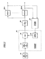
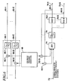
- the multiband frequency generator comprises only one frequency synthesis unit 10.
- the frequency synthesis unit 10 comprises a programmable reference divider 10, a programmable signal divider 14 and a phase detector 16.
- the input to the programmable reference divider 12 is connected to a reference oscillator 18. Further, the output terminal of the programmable reference divider 12 and the output terminal of the programmable signal divider 14 are connected to the input terminals of the phase detector 16, respectively.
- the output terminal of the phase detector 16 is connected to the input terminal of a loop filter 20 provided for all frequency bands in common such that the output signal of the loop filter 20 is supplied to the different voltage-controlled oscillators 22-1 to 22-N as correcting variable or equivalently as controller output.
- the output terminals of the voltage-controlled oscillator 22-1, ..., 22-N are connected to the input terminal of the programmable signal divider 14 in the frequency synthesis unit 10 via a coupling network 24.
- the frequency band is determined on the one hand through the selection of the power supply for the voltage-controlled oscillators 22-1, ..., 22-N and on the other hand through the programming of the programmable reference divider 12. Therefore, at every time one of the voltage-controlled oscillators 22-1, ..., 22-N outputs an output signal at a frequency which is controlled according to the frequency control input signal provided through the reference oscillator 18 and the programmable reference divider 12.
- the output signal of the coupling network 24 is forwarded to the second programmable signal divider 14 adapted through appropriate programming to re-convert the output signal of the activated voltage-controlled oscillator 22-1, ..., 22-N into the range of the frequency control input signal. Then, the phase detector 16 derives the phase difference between the frequency control input signal at the output of the programmable reference divider 12 and the output signal of the programmable signal divider 14.
- This phase difference is then supplied to a loop filter 20 with integrating characteristics.
- the output signal of this loop filter 20 is used to control the activated voltage-controlled oscillator 22-1, ..., 22-N such that the phase difference at the output of the phase detector 10 is at least constant, i.e. the frequency of the output signal of the activated voltage-controlled oscillator 22-1, ..., 22-N after division through the programmable signal divider 14 is coincident to the frequency of the frequency control input signal.
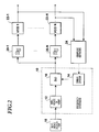
- Fig. 2 shows a schematic diagram of a second embodiment of the multiband frequency generator.
- circuit components having a functionality being identical to that of components shown in Fig. 1 are denoted using the same reference numerals.
- each voltage-controlled oscillator 22-1, ..., 22-N there is provided a dedicated loop filter 20-1, ..., 20-N.
- this phase difference is supplied to a loop filter 20-1, ..., 20-N specifically provided for each frequency band.
- the output signal of each loop filter 20-1, ..., 20-N is then used to control the related voltage-controlled oscillator 22-1, ..., 22-N such that the frequency resulting from a division of the output signal frequency of the related voltage-controlled oscillator 22-1, ..., 22-N is coincident to the frequency control input signal.
- the second embodiment of the present invention enables a specific tuning of the transient behaviour and the stability of each voltage-controlled oscillator.
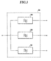
- Fig. 3 shows a schematic diagram of the coupling network 24 shown in Fig. 1.
- This coupling network 24 is implemented as filter bank and comprises at least two elements taken from a group consisting of a high pass filter 26, a band pass filter 28 and a low pass filter 30.
- the coupling network 24 and the filter component comprised therein achieves an effective decoupling between the different voltage-controlled oscillator units 22-1, ..., 22-N of the voltage-controlled multiband oscillator, both, for the first and second embodiment of the present invention.
- the coupling network 24 enables an impedance matching between different voltage-controlled oscillators 22-1, ..., 22-N and the input impedance of the programmable signal divider 14. Further, through appropriate design the loss between each voltage-controlled oscillator 22-1, ..., 22-N and the phase-locked loop circuit consisting of the frequency synthesis unit 10 and the loop filter 20 is minimized.
- Fig. 4 shows a specific implementation of the coupling network 24 for a dual band operation.
- This coupling network 24 comprises a high pass filter and a low pass filter.
- the high pass filter consists of a first capacitor 32 connected in series and a first inductivity 34 connected thereto in parallel.
- the low pass filter consists of an inductivity 36 connected in series and a second capacitor 38 connected in parallel.
- a third capacitor 40 At a branch point between the second inductivity 36 and the second capacitor 38 there is connected a third capacitor 40 in series.
- the cutoff frequency of the high pass filter with the first capacitor 32 and the first inductivity 34 lies above the signal frequency of the voltage-controlled oscillator in the lower frequency band.
- the first capacitor 32 shortcuts signals in the higher frequency range while signal components of lower frequency are branched off through the first inductivity 34. Further, the first capacitor 32 and the first inductivity 34 enable an impedance matching between the related voltage-controlled oscillator and the input terminal of the programmable signal divider 14.
- the second inductivity 36 shown in Fig. 4 forwards signal components with lower frequencies to the programmable signal divider 14 while signal components in the higher frequency ranges are shortcut through the second capacitor 38 to ground.
- the third capacitor 40 is provided for a DC-decoupling.
- the second inductivity 36 and the second capacitor 38 also enable an impedance matching between the related voltage-controlled oscillator and the input terminal of the programmable signal divider 14.
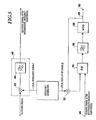
- Fig. 5 shows the basic principle underlying the application of the multiband frequency generator according to the present invention.
- a local oscillator signal is generated in a frequency generator and this local oscillator signal is used in a mixer stage 40 comprising a multiplier 42 and a band pass 44 for the conversion of the receiving signal in a receiving intermediate frequency range.
- the approach is similar to the approach explained with reference to Fig. 8 that is also related to the intermediate frequency conversion of a receiving signal.
- the conversion in the sending channel is implemented in a completely different way.
- a sending terminal 46 an intermediate frequency modulated sending signal is supplied.
- a sending signal outputted via a sending output terminal 50 is supplied to a re-convert multiplier 52 via a tap 48.
- the re-convert multiplier 52 serves to re-convert the sending signal into the intermediate frequency band.
- a sending phase detector determines the phase difference between the IF-re-converted sending signal and the IF-modulated sending signal and at the same time implements a filtering of those signal components comprised in the IF-re-converted sending signal which are to be suppressed for the further processing.
- a voltage-controlled sending oscillator 58 is controlled via a loop filter 56 such that the phase difference between the IF-re-converted sending signal and the IF-modulated sending signal is used as a correcting variable, or in other words, the IF-modulated sending signal is impressed onto the output signal of the voltage-controlled sending oscillator 58.
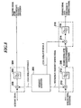
- Fig. 6 shows a first application of the multiband-frequency generator according to the present invention in a sending/ receiving unit being operated in accordance to the functional diagram explained above with respect to Fig. 5.
- a multiband-frequency generator 60 is connected to a plurality of receiving channels 62-1, ..., 62-E.
- each receiving channel 62-1, ..., 62-E there is provided a related mixing stage 64-1, ..., 64-E each comprising a multiplier 66-1, ..., 66-E and a band-pass filter 68-1, ..., 68-E, respectively.
- a suitable local oscillator signal through the multiband frequency generator 60 in accordance with the respective frequency band.
- a sending terminal 72 is provided to supply an IF-modulated sending signal which is directed towards one input terminal of a multiband sending phase detector 74 processing the IF-modulated sending signal and an IF-re-converted sending signal at every time.
- the output signal of this multiband sending phase detector 74 is supplied via a multiband loop filter to each of a plurality of voltage-controlled oscillators 78-1, ..., 78-S provided for the different sending frequency bands.
- each such voltage-controlled oscillator 78-1, ..., 78-S the related output signal is picked up with a tap 80-1, ..., 80-S to the related IF-re-conversion-multiplier 82-1, ..., 82-S provided for a re-conversion of the sending signal into the IF-frequency-band, respectively.
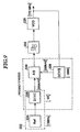
- Fig. 7 shows a second application of the multiband frequency generator according to the present invention within a sending/ receiving unit in accordance with the basic functional principle outlined above with reference to Fig. 5.
- circuit components having the same functionality as those shown in Fig. 6 are denoted with the same reference numerals.
- the second application of the multiband frequency generator according to the present invention differs from the first application explained above with reference to Fig. 6 in that there is provided a single loop filter 76-1, ..., 76-S in each sending branch 70-1, ..., 70-S to control the related voltage-controlled oscillator 78-1, ..., 78-S. Therefore, the transient behaviour and the related stability in each sending channel 70-1, ..., 70-S may be controlled and varied selectively.
Landscapes
- Engineering & Computer Science (AREA)
- Computer Networks & Wireless Communication (AREA)
- Signal Processing (AREA)
- Power Engineering (AREA)
- Stabilization Of Oscillater, Synchronisation, Frequency Synthesizers (AREA)
- Superheterodyne Receivers (AREA)
- Transceivers (AREA)
Claims (20)
- Ein Multibandfrequenzgenerator, um ein Ausgangssignal in mindestens zwei Frequenzbändern zu erzeugen, der beinhaltet:a) einen spannungsgesteuerten Multibandoszillator (22-1, ..., 22-N), um ein Ausgangssignal in jedem Frequenzband an einem einzigen Ausgangsanschluss für jedes Frequenzband zu erzeugen,b) eine Frequenzsyntheseeinrichtung (10), um einen Phasenunterschied zwischen einem Steuereingangssignal für die Frequenz und dem erzeugten Ausgangssignal abzuleiten,c) mindestens eine Steuereinrichtung (20) für den spannungsgesteuerten Multibandoszillator, die jeweils den Phasenunterschied als Korrekturvariable benutzt, der durch die Frequenzsyntheseeinrichtung (10) erzeugt wird,
gekennzeichnet dadurch, dassd) jeder Ausgangsanschluss des Multibandoszillators an die Frequenzsyntheseeinrichtung (10) über eine frequenzselektive Kopplungseinrichtung (24), die aus einer Filterbank besteht, gekoppelt ist, die angepasst ist, eine Entkopplung der verschiedenen Ausgangssignale des Multibandoszillators durch ein frequenzselektives Verhalten der Filterbank vor der Rückführung zu der Frequenzsyntheseeinrichtung (10) zu erreichen. - Ein Multibandfrequenzgenerator gemäß Anspruch 1, gekennzeichnet dadurch, dass für jedes Frequenzband eine zugeordnete Steuereinrichtung (20-1, ...,20-N) vorgesehen ist.
- Ein Multibandfrequenzgenerator gemäß einem der Ansprüche 1 und 2, gekennzeichnet dadurch, dass die Frequenzsyntheseeinrichtung (10) beinhaltet:e) einen ersten, programmierbaren Referenzdividierer (12), um das Steuereingangssignal durch Teilen der Frequenz eines vorher festgelegten Referenzsignals abzuleiten,f) einen zweiten, programmierbaren Signaldividierer (14), um die Frequenz des Ausgangssignals der frequenzselektiven Kopplungseinrichtung (24) durch einen zuvor definierten Faktor zu teilen, undg) eine Einrichtung zum Detektieren des Phasenunterschiedes (16), um den Phasenunterschied zwischen dem Ausgangsignal des ersten, programinierbaren Referenzdividierers (12) und dem Ausgangssignal des zweiten, programmierbaren Signaldividierers (14) abzuleiten.
- Ein Multibandfrequenzgenerator gemäß einem der Ansprüche 1 oder 3, dadurch gekennzeichnet, dass die Steuereinrichtung (20) für den spannungsgesteuerten Multibandoszillator ein Schleifenfilter ist.
- Ein Multibandfrequenzgenerator gemäß den Ansprüchen 2 oder 3, dadurch gekennzeichnet, dass jede Steuereinrichtung (20-1, ..., 20-N) für den spannungsgesteuerten Multibandoszillator ein Schleifenfilter ist.
- Ein Multibandfrequenzgenerator gemäß einem der Ansprüche von 1 bis 5, dadurch gekennzeichnet, dass der spannungsgesteuerte Multibandoszillator aus einer Vielzahl von spannungsgesteuerten Einzelbandoszillatoren (22-1, ..., 22-N) besteht, die parallel verbunden sind.
- Ein Multibandfrequenzgenerator gemäß einem der Ansprüche 1 bis 6, dadurch gekennzeichnet, dass der spannungsgesteuerte Multibandoszillator ein schaltbarer, spannungsgesteuerter Oszillator ist.
- Ein Multibandfrequenzgenerator gemäß einem der Ansprüche 1 bis 7, dadurch gekennzeichnet, dass die Filterbank mindestens einen Tiefpassfilter (30) enthält.
- Ein Multibandfrequenzgenerator gemäß dem Anspruch 8, dadurch gekennzeichnet, dass die Filterbank mindestens einen Bandpassfilter (28) enthält.
- Ein Multibandfrequenzgenerator gemäß dem Anspruch 8 oder 9, dadurch gekennzeichnet, dass die Filterbank mindestens einen Hochpassfilter (26) enthält.
- Ein Multibandfrequenzgenerator gemäß einem der Ansprüche 8 bis 10, dadurch gekennzeichnet, dass der Tiefpassfilter eine erste Induktivität (36) beinhaltet, die in Serie zwischen dem Eingangsanschluss des Tiefpassfilters und dem Ausgangsanschluss des Tiefpassfilters verbunden ist und ein erster Kondensator (38) vor der ersten Induktivität (36) zur Masse abzweigt.
- Ein Multibandfrequenzgenerator gemäß dem Anspruch 11, dadurch gekennzeichnet, dass in dem Tiefpassfilter ein zweiter Kondensator (40) in Serie zwischen der ersten Induktivität (36) und dem Eingangsanschluss des Tiefpassfilters verbunden ist.
- Ein Multibandfrequenzgenerator gemäß einem der Ansprüche von 10 bis 12, dadurch gekennzeichnet, dass der Hochpassfilter (26) einen dritten Kondensator (32) enthält, der in Serie zwischen dem Eingangsanschluss des Hochpassfilters und dem Ausgangsanschluss des Hochpassfilters verbunden ist und eine zweite Induktivität (34) vor dem dritten Kondensator (32) zur Masse abzweigt.
- Eine Sende/Empfangseinheit für eine mobile Radioeinheit mit Multibandbetrieb, die beinhaltet:a) mindestens einen Empfangszweig (62-1, ..., 62-E) für jedes Empfangsfrequenzband mit einer Mixerstufe, zu dem ein erstes, lokales Oszillatorsignal in einer geeigneten Art und Weise zugeführt wird,b) mindestens einen Übertragungszweig (70-1, ..., 70-S) für jedes Übertragungsfrequenzband, in dem ein zwischenfrequenzmoduliertes Sendesignal in das Sendefrequenzband konvertiert wird,
dadurch gekennzeichnet, dassc) die Konvertierung in das Sendefrequenzband durch einen Phasenvergleich des zwischenfrequenzmodulierten Sendesignals mit einem Sendesignal, das in ein Zwischenfrequenzband zurückkonvertiert wird, und durch die Steuerung eines spannungsgesteuerten Oszillators (78-1, ..., 78-S) in Übereinstimmung mit dem Phasenunterschied erreicht wird, undd) ein Multibandfrequenzgenerator gemäß einem der Ansprüche 1 bis 13, der ausgefertigt ist, die lokalen Oszillatorsignale zu erzeugen. - Eine Sende/Empfangseinheit gemäß Anspruch 14, dadurch gekennzeichnet, dass der Übertragungszweig für jedes Übertragungsfrequenzband beinhaltet:a) einen Phasendetektor (74) zum Erzeugen des Frequenzunterschiedes zwischen dem zwischenfrequenzmodulierten Sendesignal und dem Sendesignal, das in die Zwischenfrequenz am Ausgang des Übertragungszweigs zurückkonvertiert wird, undb) einen Schleifenfilter (76) zum Zuführen des Phasenunterschiedes, der durch den Phasenvergleich erzeugt wird, zu dem spannungsgesteuerten Oszillator des Übertragungszweiges.
- Eine Sende/Empfangseinheit gemäß Anspruch 15, dadurch gekennzeichnet, dass der Phasendetektor und der Schleifenfilter für jeden Übertragungszweig für jeden Übertragungszweig gemeinsam sind.
- Eine Sende/Empfangseinheit gemäß Anspruch 15, dadurch gekennzeichnet, dass für jeden Übertragungszweig ein Schleifenfilter (76-1, ...,76-S) vorgesehen ist.
- Eine Sende/Empfangseinheit gemäß einem der Ansprüche 14 bis 17, dadurch gekennzeichnet, dass in jedem Übertragungszweig eine Multiplikationseinrichtung (82-1, ..., 82-S) vorgesehen ist, um das Ausgangssignal der verschiedenen Sendekanäle durch Multiplikation mit einem verwandten, zweiten, lokalen Oszillatorsignal zurückzukonvertieren.
- Ein Verfahren zum Betreiben eines Multibandfrequenzgenerators, um ein Ausgangssignal in mindestens zwei Frequenzbändern zu erzeugen, das die Schritte beinhaltet:a) Ausgabe des Ausgangssignals über eine Ausgabe eines spannungsgesteuerten Multibandoszillators (22-1, ..., 22-N) für jedes Frequenzband,b) Ableiten eines Phasenunterschiedes zwischen einem Frequenzsteuereingangssignal und dem erzeugten Ausgangssignal in einer Frequenzsyntheseeinrichtung (10),c) Steuerung des spannungsgesteuerten MultibandOszillators (22-1, ..., 22-N) durch Verwenden des Phasenunterschiedes als korrigierende Variable,
dadurch gekennzeichnet, dass dieses weiter den Schritt beinhaltet:d) Koppeln des Ausgangssignals am Ausgangsanschluss des spannungsgesteuerten Multibandoszillators (22-1, ..., 22-N) über eine frequenzselektive Kopplungseinrichtung (24), die aus einer Filterbank besteht, die angepasst ist, ein Entkoppeln der verschiedenen Multibandausgangssignale durch ein frequenzselektives Verhalten der Filterbank vor der Rückführung zu der Frequenzsyntheseeinrichtung (10) zu erreichen. - Ein Verfahren gemäß Anspruch 19, dadurch gekennzeichnet, dass die Auswahl des Frequenzbandes durch das An- beziehungsweise das Ausschalten einer verwandten Einheit in dem spannungsgesteuerten Multibandoszillator (22-1, ..., 22-N) und weiter durch eine geeignete Definition des Frequenzsteuereingangssignals erreicht wird.
Applications Claiming Priority (3)
| Application Number | Priority Date | Filing Date | Title |
|---|---|---|---|
| DE19823103 | 1998-05-22 | ||
| DE19823103A DE19823103C2 (de) | 1998-05-22 | 1998-05-22 | Mehrfachband-Frequenzgenerierung mit einer PLL-Schaltung |
| PCT/EP1999/003529 WO1999062178A1 (en) | 1998-05-22 | 1999-05-21 | Multiband frequency generation using a single pll-circuit |
Publications (2)
| Publication Number | Publication Date |
|---|---|
| EP1078467A1 EP1078467A1 (de) | 2001-02-28 |
| EP1078467B1 true EP1078467B1 (de) | 2007-04-04 |
Family
ID=7868724
Family Applications (1)
| Application Number | Title | Priority Date | Filing Date |
|---|---|---|---|
| EP99927747A Expired - Lifetime EP1078467B1 (de) | 1998-05-22 | 1999-05-21 | Mehrfachband-frequenzgenerierung mit einer einzigen pll-schaltung |
Country Status (10)
| Country | Link |
|---|---|
| EP (1) | EP1078467B1 (de) |
| JP (1) | JP2002517118A (de) |
| KR (1) | KR100686440B1 (de) |
| CN (1) | CN1205752C (de) |
| AU (1) | AU754623B2 (de) |
| BR (1) | BR9910654A (de) |
| DE (1) | DE19823103C2 (de) |
| EE (1) | EE200000673A (de) |
| HK (1) | HK1039695B (de) |
| WO (1) | WO1999062178A1 (de) |
Families Citing this family (6)
| Publication number | Priority date | Publication date | Assignee | Title |
|---|---|---|---|---|
| US6731712B1 (en) | 2000-02-04 | 2004-05-04 | Conexant Systems, Inc. | Fully integrated broadband tuner |
| JP3873671B2 (ja) * | 2001-06-12 | 2007-01-24 | ソニー株式会社 | 通信装置 |
| KR100516916B1 (ko) | 2003-05-22 | 2005-09-27 | 한국전자통신연구원 | 시간지연과 파형 변환을 이용한 펄스 발생장치 및 그방법과 그를 이용한 다중 주파수 대역폭 무선통신시스템의 송신장치 |
| KR100910531B1 (ko) * | 2007-09-11 | 2009-07-31 | 삼성전기주식회사 | 다중 대역 전압 제어 발진기를 갖는 주파수 합성기 |
| KR101007211B1 (ko) * | 2010-05-01 | 2011-01-12 | 삼성탈레스 주식회사 | 항공전자용 광대역 고주파 주파수 합성기 |
| CN104660252B (zh) * | 2013-11-22 | 2019-08-02 | 苏州普源精电科技有限公司 | 一种具有相位调节功能的射频信号源 |
Family Cites Families (12)
| Publication number | Priority date | Publication date | Assignee | Title |
|---|---|---|---|---|
| DE2607530C2 (de) * | 1976-02-25 | 1986-12-18 | Robert Bosch Gmbh, 7000 Stuttgart | Funkgerät mit einer Oszillatoren-Einrichtung |
| JPS5843632A (ja) * | 1981-09-01 | 1983-03-14 | テクトロニツクス・インコ−ポレイテツド | 位相固定回路 |
| US4629999A (en) * | 1983-12-27 | 1986-12-16 | North American Philips Corp. | Phase-locked loop capable of generating a plurality of stable frequency signals |
| JPS61294936A (ja) * | 1985-06-21 | 1986-12-25 | Nec Corp | シンセサイザ− |
| FR2685583B1 (fr) * | 1991-12-23 | 1997-01-03 | Applic Gles Electr Meca | Synthetiseur de frequences multibande. |
| JP3014566B2 (ja) * | 1992-06-22 | 2000-02-28 | 松下電器産業株式会社 | Pll回路 |
| KR940005459A (ko) * | 1992-06-22 | 1994-03-21 | 모리시타 요이찌 | Pll회로 |
| US5686864A (en) * | 1995-09-05 | 1997-11-11 | Motorola, Inc. | Method and apparatus for controlling a voltage controlled oscillator tuning range in a frequency synthesizer |
| JPH09186587A (ja) * | 1995-12-31 | 1997-07-15 | Kenwood Corp | Pll回路 |
| GB2310342A (en) * | 1996-02-16 | 1997-08-20 | Northern Telecom Ltd | Dual mode radio transceiver front end |
| US6546044B1 (en) * | 1996-10-11 | 2003-04-08 | Ericsson Inc. | Dual-mode radiotelephone apparatus for digital or analog modulation |
| WO1998051014A1 (en) * | 1997-05-02 | 1998-11-12 | Analog Devices, Inc. | Dual band phase locked loop using independent charge pumps |
-
1998
- 1998-05-22 DE DE19823103A patent/DE19823103C2/de not_active Expired - Lifetime
-
1999
- 1999-05-21 HK HK02101242.2A patent/HK1039695B/zh not_active IP Right Cessation
- 1999-05-21 JP JP2000551483A patent/JP2002517118A/ja active Pending
- 1999-05-21 AU AU45001/99A patent/AU754623B2/en not_active Expired
- 1999-05-21 WO PCT/EP1999/003529 patent/WO1999062178A1/en not_active Ceased
- 1999-05-21 EE EEP200000673A patent/EE200000673A/xx unknown
- 1999-05-21 CN CNB998088110A patent/CN1205752C/zh not_active Expired - Lifetime
- 1999-05-21 EP EP99927747A patent/EP1078467B1/de not_active Expired - Lifetime
- 1999-05-21 BR BR9910654-0A patent/BR9910654A/pt not_active IP Right Cessation
- 1999-05-21 KR KR1020007013093A patent/KR100686440B1/ko not_active Expired - Lifetime
Also Published As
| Publication number | Publication date |
|---|---|
| AU4500199A (en) | 1999-12-13 |
| AU754623B2 (en) | 2002-11-21 |
| EP1078467A1 (de) | 2001-02-28 |
| DE19823103A1 (de) | 1999-12-09 |
| HK1039695B (zh) | 2006-01-27 |
| JP2002517118A (ja) | 2002-06-11 |
| KR100686440B1 (ko) | 2007-02-23 |
| CN1205752C (zh) | 2005-06-08 |
| BR9910654A (pt) | 2001-01-30 |
| DE19823103C2 (de) | 2002-09-26 |
| CN1309836A (zh) | 2001-08-22 |
| EE200000673A (et) | 2002-04-15 |
| WO1999062178A1 (en) | 1999-12-02 |
| HK1039695A1 (en) | 2002-05-03 |
| KR20010034884A (ko) | 2001-04-25 |
Similar Documents
| Publication | Publication Date | Title |
|---|---|---|
| US6785525B2 (en) | Multiband frequency generation using a single PLL-circuit | |
| US6538521B2 (en) | Voltage controlled oscillator | |
| KR20010015530A (ko) | 다중 모드 직접 변환 수신기 | |
| EP0781475A1 (de) | Dual-mode satelliten/zellulares-telefon mit einem frequenzsynthetisierer | |
| US6026307A (en) | Arrangement in a communication system | |
| JP2001024543A (ja) | 送受信機 | |
| WO1989007865A1 (en) | Bandswitching a two-way radio having a pll | |
| WO2004082160A1 (en) | Mutti-band frequency synthesizer | |
| WO1998036491A1 (en) | Voltage controlled ring oscillator frequency multiplier | |
| WO2001043288A1 (en) | Ring oscillator with jitter reset | |
| US6112068A (en) | Phase-locked loop circuit with switchable outputs for multiple loop filters | |
| EP1078467B1 (de) | Mehrfachband-frequenzgenerierung mit einer einzigen pll-schaltung | |
| US6175281B1 (en) | PLL frequency synthesizer and portable terminal employing the PLL frequency synthesizer | |
| EP1292038A2 (de) | Sendeverfahren und Sendegerät und Frequenzplanung zur Reduktion der Interferenzsignale | |
| EP0943180A1 (de) | Mehrkanaliges funkgerät, funkkommunikationssystem und frequenzsynthetisierer mit gebrochenem teilverhältnis | |
| US7020230B2 (en) | Frequency synthesizer for dual mode receiver | |
| GB2373113A (en) | Improvements in or relating to fast frequency-hopping synthesisers | |
| JP5133893B2 (ja) | 共有発振器を有する信号調整回路 | |
| KR100293442B1 (ko) | 디지털 주파수 공용통신 단말기의 주파수 신서사이저 장치 | |
| JPH03504661A (ja) | Pllを有する2ウエイ無線機の帯域切替 | |
| JP2002164784A (ja) | 周波数発生回路 | |
| JP2000165279A (ja) | Fm受信回路における受信トラッキング補正回路 | |
| HK1029461B (en) | A multi-band communication receiver and a method for receiving a communication signal | |
| HK1124442A (en) | Frequency generator with multiple voltage-controlled oscillators |
Legal Events
| Date | Code | Title | Description |
|---|---|---|---|
| PUAI | Public reference made under article 153(3) epc to a published international application that has entered the european phase |
Free format text: ORIGINAL CODE: 0009012 |
|
| 17P | Request for examination filed |
Effective date: 20001110 |
|
| AK | Designated contracting states |
Kind code of ref document: A1 Designated state(s): ES GB IT SE |
|
| RAP1 | Party data changed (applicant data changed or rights of an application transferred) |
Owner name: TELEFONAKTIEBOLAGET LM ERICSSON (PUBL) |
|
| GRAP | Despatch of communication of intention to grant a patent |
Free format text: ORIGINAL CODE: EPIDOSNIGR1 |
|
| GRAS | Grant fee paid |
Free format text: ORIGINAL CODE: EPIDOSNIGR3 |
|
| GRAL | Information related to payment of fee for publishing/printing deleted |
Free format text: ORIGINAL CODE: EPIDOSDIGR3 |
|
| GRAS | Grant fee paid |
Free format text: ORIGINAL CODE: EPIDOSNIGR3 |
|
| GRAA | (expected) grant |
Free format text: ORIGINAL CODE: 0009210 |
|
| AK | Designated contracting states |
Kind code of ref document: B1 Designated state(s): ES GB IT SE |
|
| REG | Reference to a national code |
Ref country code: GB Ref legal event code: FG4D |
|
| PG25 | Lapsed in a contracting state [announced via postgrant information from national office to epo] |
Ref country code: SE Free format text: LAPSE BECAUSE OF FAILURE TO SUBMIT A TRANSLATION OF THE DESCRIPTION OR TO PAY THE FEE WITHIN THE PRESCRIBED TIME-LIMIT Effective date: 20070704 |
|
| PG25 | Lapsed in a contracting state [announced via postgrant information from national office to epo] |
Ref country code: ES Free format text: LAPSE BECAUSE OF FAILURE TO SUBMIT A TRANSLATION OF THE DESCRIPTION OR TO PAY THE FEE WITHIN THE PRESCRIBED TIME-LIMIT Effective date: 20070715 |
|
| PLBE | No opposition filed within time limit |
Free format text: ORIGINAL CODE: 0009261 |
|
| STAA | Information on the status of an ep patent application or granted ep patent |
Free format text: STATUS: NO OPPOSITION FILED WITHIN TIME LIMIT |
|
| 26N | No opposition filed |
Effective date: 20080107 |
|
| PG25 | Lapsed in a contracting state [announced via postgrant information from national office to epo] |
Ref country code: IT Free format text: LAPSE BECAUSE OF FAILURE TO SUBMIT A TRANSLATION OF THE DESCRIPTION OR TO PAY THE FEE WITHIN THE PRESCRIBED TIME-LIMIT Effective date: 20070404 |
|
| PGFP | Annual fee paid to national office [announced via postgrant information from national office to epo] |
Ref country code: GB Payment date: 20180529 Year of fee payment: 20 |
|
| REG | Reference to a national code |
Ref country code: GB Ref legal event code: PE20 Expiry date: 20190520 |
|
| PG25 | Lapsed in a contracting state [announced via postgrant information from national office to epo] |
Ref country code: GB Free format text: LAPSE BECAUSE OF EXPIRATION OF PROTECTION Effective date: 20190520 |