EP1074036B1 - Color display device - Google Patents
Color display device Download PDFInfo
- Publication number
- EP1074036B1 EP1074036B1 EP20000904908 EP00904908A EP1074036B1 EP 1074036 B1 EP1074036 B1 EP 1074036B1 EP 20000904908 EP20000904908 EP 20000904908 EP 00904908 A EP00904908 A EP 00904908A EP 1074036 B1 EP1074036 B1 EP 1074036B1
- Authority
- EP
- European Patent Office
- Prior art keywords
- display device
- color
- color display
- phosphors
- sub
- Prior art date
- Legal status (The legal status is an assumption and is not a legal conclusion. Google has not performed a legal analysis and makes no representation as to the accuracy of the status listed.)
- Expired - Lifetime
Links
Images


Classifications
-
- H—ELECTRICITY
- H01—ELECTRIC ELEMENTS
- H01J—ELECTRIC DISCHARGE TUBES OR DISCHARGE LAMPS
- H01J11/00—Gas-filled discharge tubes with alternating current induction of the discharge, e.g. alternating current plasma display panels [AC-PDP]; Gas-filled discharge tubes without any main electrode inside the vessel; Gas-filled discharge tubes with at least one main electrode outside the vessel
- H01J11/20—Constructional details
- H01J11/34—Vessels, containers or parts thereof, e.g. substrates
- H01J11/42—Fluorescent layers
-
- C—CHEMISTRY; METALLURGY
- C09—DYES; PAINTS; POLISHES; NATURAL RESINS; ADHESIVES; COMPOSITIONS NOT OTHERWISE PROVIDED FOR; APPLICATIONS OF MATERIALS NOT OTHERWISE PROVIDED FOR
- C09K—MATERIALS FOR MISCELLANEOUS APPLICATIONS, NOT PROVIDED FOR ELSEWHERE
- C09K11/00—Luminescent, e.g. electroluminescent, chemiluminescent materials
- C09K11/08—Luminescent, e.g. electroluminescent, chemiluminescent materials containing inorganic luminescent materials
- C09K11/59—Luminescent, e.g. electroluminescent, chemiluminescent materials containing inorganic luminescent materials containing silicon
- C09K11/592—Chalcogenides
- C09K11/595—Chalcogenides with zinc or cadmium
-
- C—CHEMISTRY; METALLURGY
- C09—DYES; PAINTS; POLISHES; NATURAL RESINS; ADHESIVES; COMPOSITIONS NOT OTHERWISE PROVIDED FOR; APPLICATIONS OF MATERIALS NOT OTHERWISE PROVIDED FOR
- C09K—MATERIALS FOR MISCELLANEOUS APPLICATIONS, NOT PROVIDED FOR ELSEWHERE
- C09K11/00—Luminescent, e.g. electroluminescent, chemiluminescent materials
- C09K11/08—Luminescent, e.g. electroluminescent, chemiluminescent materials containing inorganic luminescent materials
- C09K11/77—Luminescent, e.g. electroluminescent, chemiluminescent materials containing inorganic luminescent materials containing rare earth metals
- C09K11/7766—Luminescent, e.g. electroluminescent, chemiluminescent materials containing inorganic luminescent materials containing rare earth metals containing two or more rare earth metals
- C09K11/7777—Phosphates
-
- C—CHEMISTRY; METALLURGY
- C09—DYES; PAINTS; POLISHES; NATURAL RESINS; ADHESIVES; COMPOSITIONS NOT OTHERWISE PROVIDED FOR; APPLICATIONS OF MATERIALS NOT OTHERWISE PROVIDED FOR
- C09K—MATERIALS FOR MISCELLANEOUS APPLICATIONS, NOT PROVIDED FOR ELSEWHERE
- C09K11/00—Luminescent, e.g. electroluminescent, chemiluminescent materials
- C09K11/08—Luminescent, e.g. electroluminescent, chemiluminescent materials containing inorganic luminescent materials
- C09K11/77—Luminescent, e.g. electroluminescent, chemiluminescent materials containing inorganic luminescent materials containing rare earth metals
- C09K11/7766—Luminescent, e.g. electroluminescent, chemiluminescent materials containing inorganic luminescent materials containing rare earth metals containing two or more rare earth metals
- C09K11/778—Borates
-
- G—PHYSICS
- G09—EDUCATION; CRYPTOGRAPHY; DISPLAY; ADVERTISING; SEALS
- G09G—ARRANGEMENTS OR CIRCUITS FOR CONTROL OF INDICATING DEVICES USING STATIC MEANS TO PRESENT VARIABLE INFORMATION
- G09G3/00—Control arrangements or circuits, of interest only in connection with visual indicators other than cathode-ray tubes
- G09G3/20—Control arrangements or circuits, of interest only in connection with visual indicators other than cathode-ray tubes for presentation of an assembly of a number of characters, e.g. a page, by composing the assembly by combination of individual elements arranged in a matrix no fixed position being assigned to or needed to be assigned to the individual characters or partial characters
- G09G3/22—Control arrangements or circuits, of interest only in connection with visual indicators other than cathode-ray tubes for presentation of an assembly of a number of characters, e.g. a page, by composing the assembly by combination of individual elements arranged in a matrix no fixed position being assigned to or needed to be assigned to the individual characters or partial characters using controlled light sources
- G09G3/28—Control arrangements or circuits, of interest only in connection with visual indicators other than cathode-ray tubes for presentation of an assembly of a number of characters, e.g. a page, by composing the assembly by combination of individual elements arranged in a matrix no fixed position being assigned to or needed to be assigned to the individual characters or partial characters using controlled light sources using luminous gas-discharge panels, e.g. plasma panels
- G09G3/288—Control arrangements or circuits, of interest only in connection with visual indicators other than cathode-ray tubes for presentation of an assembly of a number of characters, e.g. a page, by composing the assembly by combination of individual elements arranged in a matrix no fixed position being assigned to or needed to be assigned to the individual characters or partial characters using controlled light sources using luminous gas-discharge panels, e.g. plasma panels using AC panels
- G09G3/291—Control arrangements or circuits, of interest only in connection with visual indicators other than cathode-ray tubes for presentation of an assembly of a number of characters, e.g. a page, by composing the assembly by combination of individual elements arranged in a matrix no fixed position being assigned to or needed to be assigned to the individual characters or partial characters using controlled light sources using luminous gas-discharge panels, e.g. plasma panels using AC panels controlling the gas discharge to control a cell condition, e.g. by means of specific pulse shapes
-
- H—ELECTRICITY
- H01—ELECTRIC ELEMENTS
- H01J—ELECTRIC DISCHARGE TUBES OR DISCHARGE LAMPS
- H01J11/00—Gas-filled discharge tubes with alternating current induction of the discharge, e.g. alternating current plasma display panels [AC-PDP]; Gas-filled discharge tubes without any main electrode inside the vessel; Gas-filled discharge tubes with at least one main electrode outside the vessel
- H01J11/10—AC-PDPs with at least one main electrode being out of contact with the plasma
- H01J11/12—AC-PDPs with at least one main electrode being out of contact with the plasma with main electrodes provided on both sides of the discharge space
Definitions
- the invention relates to a color display device comprising a first substrate provided with a layer of fluorescent material, and a second, transparent substrate, said color display device comprising means for addressing pixels during use.
- the display device may be a plasma display device but also, for example, a display device of the field emission type.
- the address electrodes may be present on both the first and the second substrate in the case of a plasma display device.
- the fluorescent material is patterned or not patterned.
- a display device of this type is used, inter alia, in large-area, flat display screens, for example, for HDTV.
- a color display device (plasma display panel or PDP) of the type mentioned above is described in EP-A-0 488 891.
- This application describes measures for obtaining grey values or color gradations.
- the frame time is divided into a plurality of sub-frames having a weighted duration (for example in the ratio 1:2:4:...:128).
- a frequently used phosphor such as Zn 2 SiO 4 :Mn (willemite) exhibits saturation phenomena.
- the efficiency of the phosphor (number of emitted photons/number of incoming photons) deteriorates, so that the brightness decreases.
- an object of the present invention to provide a display device of the type described, which has an optimum brightness or luminance, also when a given color is fully driven.
- a color display device is characterized in that the layer of fluorescent material, comprises at least two different phosphors of substantially the same color at the location of a pixel.
- Substantially the same color is herein understood to mean that the difference in spectral color of the emission peaks of the phosphors. measured as the distance in C.I.E co-ordinates (x, y co-ordinates) is at most 0.35 (and preferably at most 0.25).
- the invention is based on the recognition that the decrease of the efficiency for different phosphors depends in different manners on the number of incoming photons.
- a non-saturating phosphor is herein understood to mean a phosphor in which the number of emitted photons per unit of surface and time has decreased at most 15% in the case of a drive yielding a brightness (or luminance) of 500 Cd/m 2 as compared with a drive yielding a brightness of 10 Cd/m 2 .
- Suitable non-saturating phosphors are, for example:
- a preferred embodiment of a display device is characterized in that the layer of fluorescent material at the location of a pixel, viewed in a direction transverse to the first substrate, comprises at least two sub-pixels having different phosphors of substantially the same color for different sub-pixels.
- An incoming (video) signal can now be split up, for example, into two or more sub-signals each supplying one of the sub-pixels with a separate drive signal. By means of the sub-signals, the extent of mixing of the colors is then adjusted, or a choice is made between the sub-pixels.
- Fig. 1 shows a plasma display device 10, in this case an AC display panel (AC PDP or AC Plasma Display Panel), having a first substrate 1 provided with two display electrodes 2 which are coated with a dielectric layer 3 (for example, glass), and a second, transparent substrate 5 provided with fluorescent material 8.
- the second substrate 5 is provided with address electrodes 6.
- a sub-pixel as defined by the address electrode 6 and the display electrodes 2 is bounded by partition walls 7 which bound a discharge space.
- the partition walls 7 are not absolutely necessary, while display electrodes and address electrodes may be alternatively present on one substrate.
- a gas discharge mixture 9 consisting, in this embodiment, of a helium-xenon mixture, is present in the discharge space between the substrates 1, 5.
- Other mixtures are alternatively possible, such as neon-xenon, argon-xenon, krypton-xenon, argon-neon-xenon, argon-helium-xenon, krypton-neon-xenon, krypton-helium-xenon or mixtures thereof, the quantity of xenon being in a range between 5 and less than 100%.
- UV radiation is generated in plasma display devices (plasma display panels or PDPs) in the discharge space at the area of a (sub-)pixel, which UV radiation causes the fluorescent material 8 (phosphors) to luminesce.
- the display electrodes 2 are driven, for example, from X and Y drivers 20, 21 and the address electrodes are driven from an A driver 22 (Fig. 2).
- an incoming signal 11 is stored in a frame memory 12 and in a sub-frame generator 13.
- the required pulses are generated in the processing unit 14 for the reset pulses, the ignition pulses and the sustain pulses which energize the display electrodes 2 via the X and Y drivers 20, 21, while addressing takes place via the A driver 22 controlled by an address generator 16.
- Mutual synchronization takes place via a timing control circuit 15.
- the ignition is maintained by the sustain pulses across the display electrodes within a pixel.
- the sustain frequency therefore determines, together with the grey tint, the number of times a UV photon impinges upon a phosphor.
- Fig. 3 is a diagrammatic front-elevational view of a display device, particularly the location of a number of phosphors 8, 8', 8", 8"' with the colors red (R), green (G 1 ), blue (B) and a second color green (G 2 ).
- the broken line 25 diagrammatically represents a pixel.
- the C.I.E. color triangle of Fig. 4 shows the luminances associated with these phosphors as B(Y 1 ), R(Y 2 ), G 1 (Y 3 ) and G 2 (Y 4 ) (Y: luminance) in this color triangle.
- B(Y 1 ), R(Y 2 ), G 1 (Y 3 ) and G 2 (Y 4 ) Y: luminance
- Y luminance
- the point Y 0 can be realized by weighted excitation of the phosphors B, R and G 1 or by weighted excitation of the phosphors B, R and G 2 .
- Y 3 (G 1 ) and Y 4 (G 2 ) is made in the device of Fig. 2 by processing information about the color to be displayed, stored in the frame memory 12, in the processing unit 14.
- this unit comprises, for example, a microprocessor or a look-up table in which the behavior (notably the efficiency of the phosphors as a function of the frequency (grey scale to be displayed) is stored.
- the X and Y drivers are supplied with drive signals for the relevant sub-pixels.
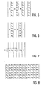
- Figs. 5 to 7 show a number of variants in which the phosphors are distributed across sub-pixels in different ways.
- a pixel 25 comprises three sub-pixels, the green sub-pixel comprising a phosphor layer G m which consists of a mixture of willemite and CBT.
- the invention is of course not limited to the embodiments described hereinbefore.
- the sub-pixels may have, for example, different surface areas, which may be incorporated in the data in the processing unit 14.
- the invention is also applicable to field emission display devices in which the efficiency of given phosphors is also dependent on the luminance to be adjusted.
- the invention relates to a luminescence-based color display device having at least one extra phosphor per pixel, in which, dependent on the color to be displayed and the luminance (brightness), the combination of sub-pixels to be driven is determined.
Priority Applications (1)
| Application Number | Priority Date | Filing Date | Title |
|---|---|---|---|
| EP20000904908 EP1074036B1 (en) | 1999-02-24 | 2000-01-10 | Color display device |
Applications Claiming Priority (4)
| Application Number | Priority Date | Filing Date | Title |
|---|---|---|---|
| EP99200520 | 1999-02-24 | ||
| EP99200520 | 1999-02-24 | ||
| EP20000904908 EP1074036B1 (en) | 1999-02-24 | 2000-01-10 | Color display device |
| PCT/EP2000/000213 WO2000051156A1 (en) | 1999-02-24 | 2000-01-10 | Color display device |
Publications (2)
| Publication Number | Publication Date |
|---|---|
| EP1074036A1 EP1074036A1 (en) | 2001-02-07 |
| EP1074036B1 true EP1074036B1 (en) | 2004-10-27 |
Family
ID=8239913
Family Applications (1)
| Application Number | Title | Priority Date | Filing Date |
|---|---|---|---|
| EP20000904908 Expired - Lifetime EP1074036B1 (en) | 1999-02-24 | 2000-01-10 | Color display device |
Country Status (7)
| Country | Link |
|---|---|
| US (1) | US6388644B1 (ko) |
| EP (1) | EP1074036B1 (ko) |
| JP (1) | JP4776078B2 (ko) |
| KR (3) | KR100898190B1 (ko) |
| DE (1) | DE60015244T2 (ko) |
| TW (1) | TW434628B (ko) |
| WO (1) | WO2000051156A1 (ko) |
Cited By (1)
| Publication number | Priority date | Publication date | Assignee | Title |
|---|---|---|---|---|
| CN101325028B (zh) * | 2002-01-07 | 2011-08-31 | 三星电子株式会社 | 彩色平板显示器的子像素排列和子像素着色设置 |
Families Citing this family (35)
| Publication number | Priority date | Publication date | Assignee | Title |
|---|---|---|---|---|
| TW533447B (en) * | 1999-12-14 | 2003-05-21 | Matsushita Electric Ind Co Ltd | Plasma display apparatus |
| DE10024835A1 (de) * | 2000-05-19 | 2001-11-22 | Philips Corp Intellectual Pty | Plasmabildschirm mit einem Terbium (III)-aktivierten Leuchtstoff |
| JP2002221935A (ja) * | 2000-11-24 | 2002-08-09 | Mitsubishi Electric Corp | 表示装置 |
| US7081928B2 (en) * | 2001-05-16 | 2006-07-25 | Hewlett-Packard Development Company, L.P. | Optical system for full color, video projector using single light valve with plural sub-pixel reflectors |
| JP4566465B2 (ja) * | 2001-06-21 | 2010-10-20 | パナソニック株式会社 | プラズマディスプレイパネル |
| JP4675517B2 (ja) * | 2001-07-24 | 2011-04-27 | 株式会社日立製作所 | プラズマディスプレイ装置 |
| AU2002353139A1 (en) | 2001-12-14 | 2003-06-30 | Clairvoyante Laboratories, Inc. | Improvements to color flat panel display sub-pixel arrangements and layouts with reduced visibility of a blue luminance well |
| US20030117423A1 (en) * | 2001-12-14 | 2003-06-26 | Brown Elliott Candice Hellen | Color flat panel display sub-pixel arrangements and layouts with reduced blue luminance well visibility |
| TWI276886B (en) * | 2002-01-07 | 2007-03-21 | Clairvoyante Inc | Improvements to color flat panel display sub-pixel arrangements and layouts for sub-pixel rendering with increased modulation transfer function response |
| JP3724430B2 (ja) * | 2002-02-04 | 2005-12-07 | ソニー株式会社 | 有機el表示装置およびその制御方法 |
| EP1388818B1 (en) * | 2002-08-10 | 2011-06-22 | Samsung Electronics Co., Ltd. | Method and apparatus for rendering image signal |
| US20040080479A1 (en) * | 2002-10-22 | 2004-04-29 | Credelle Thomas Lioyd | Sub-pixel arrangements for striped displays and methods and systems for sub-pixel rendering same |
| US7230594B2 (en) | 2002-12-16 | 2007-06-12 | Eastman Kodak Company | Color OLED display with improved power efficiency |
| US7397485B2 (en) * | 2002-12-16 | 2008-07-08 | Eastman Kodak Company | Color OLED display system having improved performance |
| US7075242B2 (en) * | 2002-12-16 | 2006-07-11 | Eastman Kodak Company | Color OLED display system having improved performance |
| US7184067B2 (en) * | 2003-03-13 | 2007-02-27 | Eastman Kodak Company | Color OLED display system |
| KR100493165B1 (ko) * | 2002-12-17 | 2005-06-02 | 삼성전자주식회사 | 영상신호 표현 방법 및 장치 |
| KR100589331B1 (ko) * | 2003-02-21 | 2006-06-14 | 삼성에스디아이 주식회사 | 플라즈마 디스플레이 패널 |
| US20040196302A1 (en) * | 2003-03-04 | 2004-10-07 | Im Moon Hwan | Systems and methods for temporal subpixel rendering of image data |
| US7091941B2 (en) | 2003-04-11 | 2006-08-15 | Eastman Kodak Company | Color OLED display with improved power efficiency |
| US7397455B2 (en) * | 2003-06-06 | 2008-07-08 | Samsung Electronics Co., Ltd. | Liquid crystal display backplane layouts and addressing for non-standard subpixel arrangements |
| US7187353B2 (en) * | 2003-06-06 | 2007-03-06 | Clairvoyante, Inc | Dot inversion on novel display panel layouts with extra drivers |
| US20040246280A1 (en) * | 2003-06-06 | 2004-12-09 | Credelle Thomas Lloyd | Image degradation correction in novel liquid crystal displays |
| US7218301B2 (en) * | 2003-06-06 | 2007-05-15 | Clairvoyante, Inc | System and method of performing dot inversion with standard drivers and backplane on novel display panel layouts |
| US8035599B2 (en) | 2003-06-06 | 2011-10-11 | Samsung Electronics Co., Ltd. | Display panel having crossover connections effecting dot inversion |
| US7209105B2 (en) * | 2003-06-06 | 2007-04-24 | Clairvoyante, Inc | System and method for compensating for visual effects upon panels having fixed pattern noise with reduced quantization error |
| US6897876B2 (en) * | 2003-06-26 | 2005-05-24 | Eastman Kodak Company | Method for transforming three color input signals to four or more output signals for a color display |
| US7084567B2 (en) * | 2003-10-20 | 2006-08-01 | .Au Optronics Corporation | Plasma display panel performing high luminance and luminous efficiency |
| JP2005227586A (ja) * | 2004-02-13 | 2005-08-25 | National Univ Corp Shizuoka Univ | 多原色ディスプレイ |
| JP2005227408A (ja) * | 2004-02-10 | 2005-08-25 | National Univ Corp Shizuoka Univ | 多原色表示装置に対する色変換方式 |
| WO2005076252A1 (ja) * | 2004-02-10 | 2005-08-18 | National University Corporation Shizuoka University | 多原色ディスプレイおよび多原色ディスプレイ用色変換方式 |
| US7333080B2 (en) * | 2004-03-29 | 2008-02-19 | Eastman Kodak Company | Color OLED display with improved power efficiency |
| GB0408486D0 (en) * | 2004-04-16 | 2004-05-19 | Koninkl Philips Electronics Nv | Electroluminescent display device |
| KR100927614B1 (ko) * | 2006-03-29 | 2009-11-23 | 삼성에스디아이 주식회사 | 플라즈마 디스플레이 패널용 적색 형광체 및 이로부터형성된 형광막을 구비하는 플라즈마 디스플레이 패널 |
| KR200453510Y1 (ko) * | 2009-02-09 | 2011-05-11 | 윤유원 | 튀김유 정제기 |
Family Cites Families (16)
| Publication number | Priority date | Publication date | Assignee | Title |
|---|---|---|---|---|
| JPS6132894A (ja) * | 1984-07-25 | 1986-02-15 | 松下電器産業株式会社 | カラ−映像表示装置 |
| ATE69332T1 (de) * | 1985-11-21 | 1991-11-15 | Gte Licht Gmbh | Niederdruckbogenentladungslichtquelleneinheit. |
| US4999791A (en) * | 1988-12-23 | 1991-03-12 | Schumann Robert W | Computer graphics color film recording method and apparatus |
| JP2995976B2 (ja) * | 1991-12-20 | 1999-12-27 | 日亜化学工業株式会社 | ランプ用緑色発光蛍光体の製造方法 |
| US5402143A (en) * | 1991-12-23 | 1995-03-28 | Panocorp Display Systems | Color fluorescent liquid crystal display |
| JP3506720B2 (ja) * | 1992-03-02 | 2004-03-15 | 三菱電機株式会社 | 気体放電表示装置 |
| JP3455267B2 (ja) * | 1994-02-14 | 2003-10-14 | パイオニア株式会社 | カラープラズマディスプレイ |
| JPH08179726A (ja) * | 1994-12-20 | 1996-07-12 | Fujitsu General Ltd | プラズマディスプレイパネル |
| JPH0963482A (ja) * | 1995-08-25 | 1997-03-07 | Fujitsu Ltd | Pdpにおける蛍光体層の形成方法 |
| JPH09208611A (ja) * | 1996-02-06 | 1997-08-12 | Japan Synthetic Rubber Co Ltd | 螢光体分散感放射線性組成物 |
| JPH09219154A (ja) * | 1996-02-08 | 1997-08-19 | Japan Synthetic Rubber Co Ltd | 螢光体組成物およびプラズマディスプレイパネル |
| KR100197579B1 (ko) * | 1996-12-03 | 1999-06-15 | 손욱 | 이중층 형광막 및 그의 제조방법 |
| JPH10302666A (ja) * | 1997-04-25 | 1998-11-13 | Toshiba Corp | カラー受像管およびその製造方法 |
| JPH10308183A (ja) * | 1997-05-09 | 1998-11-17 | Sony Corp | カラー陰極線管 |
| DE19827252A1 (de) * | 1997-06-19 | 1999-02-18 | Kasei Optonix | Seltenerdborat-Leuchtstoff |
| JP4151104B2 (ja) * | 1998-03-31 | 2008-09-17 | 株式会社日立製作所 | プラズマディスプレイ |
-
1999
- 1999-12-16 TW TW088122111A patent/TW434628B/zh not_active IP Right Cessation
-
2000
- 2000-01-10 WO PCT/EP2000/000213 patent/WO2000051156A1/en active IP Right Grant
- 2000-01-10 JP JP2000601669A patent/JP4776078B2/ja not_active Expired - Lifetime
- 2000-01-10 EP EP20000904908 patent/EP1074036B1/en not_active Expired - Lifetime
- 2000-01-10 KR KR1020077004712A patent/KR100898190B1/ko active IP Right Grant
- 2000-01-10 DE DE60015244T patent/DE60015244T2/de not_active Expired - Lifetime
- 2000-01-10 KR KR1020007011742A patent/KR20010071169A/ko not_active Application Discontinuation
- 2000-02-22 US US09/510,143 patent/US6388644B1/en not_active Expired - Lifetime
-
2008
- 2008-02-21 KR KR1020087004174A patent/KR100919959B1/ko not_active IP Right Cessation
Cited By (1)
| Publication number | Priority date | Publication date | Assignee | Title |
|---|---|---|---|---|
| CN101325028B (zh) * | 2002-01-07 | 2011-08-31 | 三星电子株式会社 | 彩色平板显示器的子像素排列和子像素着色设置 |
Also Published As
| Publication number | Publication date |
|---|---|
| EP1074036A1 (en) | 2001-02-07 |
| KR20010071169A (ko) | 2001-07-28 |
| DE60015244D1 (de) | 2004-12-02 |
| KR100919959B1 (ko) | 2009-10-01 |
| JP2002538582A (ja) | 2002-11-12 |
| DE60015244T2 (de) | 2006-03-09 |
| KR20080021164A (ko) | 2008-03-06 |
| JP4776078B2 (ja) | 2011-09-21 |
| WO2000051156A1 (en) | 2000-08-31 |
| TW434628B (en) | 2001-05-16 |
| KR100898190B1 (ko) | 2009-05-18 |
| KR20070033480A (ko) | 2007-03-26 |
| US6388644B1 (en) | 2002-05-14 |
Similar Documents
| Publication | Publication Date | Title |
|---|---|---|
| EP1074036B1 (en) | Color display device | |
| JP3529737B2 (ja) | プラズマディスプレイパネルの駆動方法および表示装置 | |
| US6577070B2 (en) | AC type plasma display panel | |
| JP3797084B2 (ja) | プラズマディスプレイ装置 | |
| KR20030036017A (ko) | 플라즈마 디스플레이 표시장치, 발광장치 및 그것을이용한 영상표시 시스템 | |
| US6034655A (en) | Method for controlling white balance in plasma display panel device | |
| JP2003036793A (ja) | プラズマカラースクリーン | |
| US6057643A (en) | Discharge gas mixture for a fluorescent gas-discharge plasma display panel | |
| JP3010658B2 (ja) | プラズマディスプレイパネルと駆動方法 | |
| JP4058299B2 (ja) | プラズマディスプレイパネル表示装置とその駆動方法 | |
| JP2003007215A (ja) | プラズマディスプレイパネル | |
| US6222324B1 (en) | Plasma display panel | |
| JP3476234B2 (ja) | プラズマディスプレイパネル及び駆動方法 | |
| JPH07245062A (ja) | プラズマディスプレイパネル | |
| JP3019025B2 (ja) | カラープラズマディスプレイパネルおよびその駆動方法 | |
| KR100205934B1 (ko) | 칼라 플라즈마 표시소자 | |
| JP3721710B2 (ja) | プラズマディスプレイパネルおよびその階調表示方法 | |
| KR100575631B1 (ko) | 칼러 플라즈마 디스플레이 패널소자 | |
| JP2001229835A (ja) | プラズマディスプレイパネル | |
| JP2001084911A (ja) | プラズマディスプレイ装置 | |
| JP2005032721A (ja) | 自発光型カラーディスプレイ装置およびその駆動方法 | |
| JP2002343258A (ja) | プラズマディスプレイパネル | |
| KR20080049945A (ko) | 플라즈마 디스플레이 패널 | |
| JP2001357785A (ja) | プラズマディスプレイ装置及びそれを用いた表示システム |
Legal Events
| Date | Code | Title | Description |
|---|---|---|---|
| PUAI | Public reference made under article 153(3) epc to a published international application that has entered the european phase |
Free format text: ORIGINAL CODE: 0009012 |
|
| AK | Designated contracting states |
Kind code of ref document: A1 Designated state(s): AT BE CH CY DE DK ES FI FR GB GR IE IT LI LU MC NL PT SE |
|
| 17P | Request for examination filed |
Effective date: 20010228 |
|
| GRAP | Despatch of communication of intention to grant a patent |
Free format text: ORIGINAL CODE: EPIDOSNIGR1 |
|
| GRAS | Grant fee paid |
Free format text: ORIGINAL CODE: EPIDOSNIGR3 |
|
| GRAA | (expected) grant |
Free format text: ORIGINAL CODE: 0009210 |
|
| AK | Designated contracting states |
Kind code of ref document: B1 Designated state(s): DE FR GB NL |
|
| PG25 | Lapsed in a contracting state [announced via postgrant information from national office to epo] |
Ref country code: NL Free format text: LAPSE BECAUSE OF FAILURE TO SUBMIT A TRANSLATION OF THE DESCRIPTION OR TO PAY THE FEE WITHIN THE PRESCRIBED TIME-LIMIT Effective date: 20041027 |
|
| REG | Reference to a national code |
Ref country code: GB Ref legal event code: FG4D |
|
| REG | Reference to a national code |
Ref country code: GB Ref legal event code: 746 Effective date: 20041101 |
|
| REG | Reference to a national code |
Ref country code: IE Ref legal event code: FG4D |
|
| REF | Corresponds to: |
Ref document number: 60015244 Country of ref document: DE Date of ref document: 20041202 Kind code of ref document: P |
|
| NLV1 | Nl: lapsed or annulled due to failure to fulfill the requirements of art. 29p and 29m of the patents act | ||
| PLBE | No opposition filed within time limit |
Free format text: ORIGINAL CODE: 0009261 |
|
| STAA | Information on the status of an ep patent application or granted ep patent |
Free format text: STATUS: NO OPPOSITION FILED WITHIN TIME LIMIT |
|
| ET | Fr: translation filed | ||
| 26N | No opposition filed |
Effective date: 20050728 |
|
| REG | Reference to a national code |
Ref country code: FR Ref legal event code: D6 |
|
| REG | Reference to a national code |
Ref country code: GB Ref legal event code: 732E Free format text: REGISTERED BETWEEN 20100204 AND 20100211 |
|
| REG | Reference to a national code |
Ref country code: FR Ref legal event code: TP |
|
| REG | Reference to a national code |
Ref country code: GB Ref legal event code: 732E Free format text: REGISTERED BETWEEN 20150220 AND 20150225 |
|
| REG | Reference to a national code |
Ref country code: DE Ref legal event code: R082 Ref document number: 60015244 Country of ref document: DE Representative=s name: KLINSKI, ROBERT, DIPL.-ING. DR.-ING., DE |
|
| REG | Reference to a national code |
Ref country code: FR Ref legal event code: TP Owner name: INTELLECTUAL KEYSTONE TECHNOLOGY LLC, US Effective date: 20150401 |
|
| REG | Reference to a national code |
Ref country code: DE Ref legal event code: R081 Ref document number: 60015244 Country of ref document: DE Owner name: INTELLECTUAL KEYSTONE TECHNOLOGY LLC, MCLEAN, US Free format text: FORMER OWNER: SAMSUNG SDI CO., LTD., SUWON, KYONGGI-DO, KR Effective date: 20150408 Ref country code: DE Ref legal event code: R082 Ref document number: 60015244 Country of ref document: DE Representative=s name: KLINSKI, ROBERT, DIPL.-ING. DR.-ING., DE Effective date: 20150408 Ref country code: DE Ref legal event code: R082 Ref document number: 60015244 Country of ref document: DE Representative=s name: VENNER SHIPLEY LLP, GB Effective date: 20150408 |
|
| REG | Reference to a national code |
Ref country code: DE Ref legal event code: R082 Ref document number: 60015244 Country of ref document: DE Representative=s name: VENNER SHIPLEY LLP, GB |
|
| REG | Reference to a national code |
Ref country code: FR Ref legal event code: PLFP Year of fee payment: 17 |
|
| REG | Reference to a national code |
Ref country code: FR Ref legal event code: PLFP Year of fee payment: 18 |
|
| REG | Reference to a national code |
Ref country code: FR Ref legal event code: PLFP Year of fee payment: 19 |
|
| PGFP | Annual fee paid to national office [announced via postgrant information from national office to epo] |
Ref country code: FR Payment date: 20181224 Year of fee payment: 20 Ref country code: GB Payment date: 20181220 Year of fee payment: 20 |
|
| PGFP | Annual fee paid to national office [announced via postgrant information from national office to epo] |
Ref country code: DE Payment date: 20181219 Year of fee payment: 20 |
|
| REG | Reference to a national code |
Ref country code: DE Ref legal event code: R071 Ref document number: 60015244 Country of ref document: DE |
|
| REG | Reference to a national code |
Ref country code: GB Ref legal event code: PE20 Expiry date: 20200109 |
|
| PG25 | Lapsed in a contracting state [announced via postgrant information from national office to epo] |
Ref country code: GB Free format text: LAPSE BECAUSE OF EXPIRATION OF PROTECTION Effective date: 20200109 |