EP1072093B1 - Schaltung zum abschalten einer mosfet-endstufe - Google Patents
Schaltung zum abschalten einer mosfet-endstufe Download PDFInfo
- Publication number
- EP1072093B1 EP1072093B1 EP98947355A EP98947355A EP1072093B1 EP 1072093 B1 EP1072093 B1 EP 1072093B1 EP 98947355 A EP98947355 A EP 98947355A EP 98947355 A EP98947355 A EP 98947355A EP 1072093 B1 EP1072093 B1 EP 1072093B1
- Authority
- EP
- European Patent Office
- Prior art keywords
- line
- mosfet
- monitoring
- output stage
- potential
- Prior art date
- Legal status (The legal status is an assumption and is not a legal conclusion. Google has not performed a legal analysis and makes no representation as to the accuracy of the status listed.)
- Expired - Lifetime
Links
- 238000012544 monitoring process Methods 0.000 claims description 22
- 230000002159 abnormal effect Effects 0.000 claims description 7
- 238000000034 method Methods 0.000 claims 2
- 230000001419 dependent effect Effects 0.000 claims 1
- 230000001681 protective effect Effects 0.000 claims 1
- 238000001514 detection method Methods 0.000 description 29
- 230000006870 function Effects 0.000 description 5
- 230000000694 effects Effects 0.000 description 2
- 230000005855 radiation Effects 0.000 description 2
- 230000006378 damage Effects 0.000 description 1
- 230000005670 electromagnetic radiation Effects 0.000 description 1
- 230000003993 interaction Effects 0.000 description 1
- 230000007257 malfunction Effects 0.000 description 1
- 230000009993 protective function Effects 0.000 description 1
Images


Classifications
-
- H—ELECTRICITY
- H03—ELECTRONIC CIRCUITRY
- H03K—PULSE TECHNIQUE
- H03K17/00—Electronic switching or gating, i.e. not by contact-making and –breaking
- H03K17/08—Modifications for protecting switching circuit against overcurrent or overvoltage
- H03K17/082—Modifications for protecting switching circuit against overcurrent or overvoltage by feedback from the output to the control circuit
- H03K17/0822—Modifications for protecting switching circuit against overcurrent or overvoltage by feedback from the output to the control circuit in field-effect transistor switches
Definitions
- the invention is based on a circuit for switching off a MOSFET output stage according to the preamble of Claim 1.
- EP 0 294 887 describes a circuit arrangement for Driving a MOSFET output stage, with a Switch-off transistor is provided, its function can be overridden.
- EP 0 602 708 discloses a circuit arrangement for Control of a power transistor with means for Monitoring an internal ground line.
- the circuit according to the invention for switching off a MOSFET output stage includes means for controlling the MOSFET POWER STAGE - the following as system logic are referred to - means of monitoring one or several lines - the following as detection logic are referred to, the detection logic being designed in this way is that they are not just the occurrence of abnormal potentials recognizes on the monitored lines, but in this Cases also the MOSFET output stage independent of the system logic off. With the detection logic, therefore, in addition to that provided within the framework of the system logic Shutdown option Another shutdown option realized of which only when abnormal occurs Potentials monitored by the detection logic Lines is used.
- the circuit has a detection logic Bipolar transistor comprising means for comparing the Potential of the monitored line with a Comparison potential. If the discrepancy between the Potential of the monitored line and the Comparison potential exceeds a predetermined level, the MOSFET output stage via the detection logic switched off.
- the detection logic of the circuit according to the invention is like this connected to the MOSFET output stage so that it can be switched off of the MOSFET output stage simply gate and source of the MOSFET output stage shorts.
- the detection logic has means for Monitoring the current between the monitored line and a defined potential.
- the MOSFET power amplifier switched off by the detection logic whenever the Current exceeds or falls below a predetermined value.
- the detection logic is the circuit according to the invention designed that the MOSFET output stage after switching off through the detection logic only after a certain Delay is released again, i.e. again can be switched on. This can cause a high frequency Switching the MOSFET output stage on / off when oscillating potentials on the monitored line, for example caused by EMC radiation can be avoided.
- the detection logic comprises means with which is the switch-off function for the MOSFET output stage when Overvoltages can be overridden. This can cause surges be dismantled via the power amplifier.
- circuit according to the invention in the monitoring of the internal ground potential, i.e. of the ground potential the means for controlling the MOSFET output stage, hereinafter referred to as system logic be designated.
- system logic the means for controlling the MOSFET output stage, hereinafter referred to as system logic.
- FIG. 1 shows the essential components of a circuit according to the invention and their interaction.
- a MOSFET power amplifier here in the form of a Power-Mos 1 is realized, is controlled via a system logic 2, which is the usual Control and protection circuits as well as application-specific functions contains.
- the Power-Mos 1 can through the system logic 2 via the switch-off path I can be turned off by the gate of Power-Mos 1 after Ground, namely to the on-chip ground potential, is switched. comes in this configuration there is an increase in the on-chip ground potential, For example, by EMC radiation or cable break, this is a clear shutdown of the Power-Mos 1 is no longer guaranteed.
- the circuit shown here therefore comprises means 3 for Monitoring the chip-internal ground line 4, which is referred to below as detection logic 3 are referred to.
- Detection logic 3 detects an abnormal potential on the ground line 4, it causes the Power-Mos 1 to be switched off.
- the gate and source of Power-Mos 1 are switched off via switch-off path II shorted.
- the monitoring of the ground line 4 is carried out here by comparison the potential of the ground line 4 with a reference signal, namely the potential of an external ground connection 5. Is the potential of the monitored ground line 4 by a certain amount above the reference potential, then the Power-Mos 1 is switched off.
- the detection logic 3 is also designed so that the Power-Mos 1 after a switch-off by the detection logic 3 only after a certain time Delay is released. This enables high-frequency on / off switching of the Power-Mos 1 due to oscillating potentials on the Avoid on-chip ground line 4.
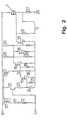
- FIG. 2 now shows the circuitry implementation of a detection logic, with which the chip-internal ground line 4 is monitored. This line connection is identified by 6 in FIG.
- the elements are between the positive supply 9 and the chip mass 4 MOSFET 10, resistor 11 and diode 12 arranged. These form together with the MOSFET 13 a current mirror, via which a current is fed in at point 14 becomes. Between point 14 and the source of the MOSFET output stage 1 and the load output 15 are the elements Resistor 16, MOSFET 17 and protection diode 18. The voltage between the Point 14 and the load output 15 determine the switching state of a MOSFET 19, whose drain connection with a pull-up resistor 20 and the gate of a MOSFET 21 is connected. The MOSFET 21 is between the gate and Source of the MOSFET output stage 1.
- the MOSFET 17 is driven via a bipolar transistor 22 and a voltage divider through the resistors 23 and 24 and the diode 25 is formed.
- the base terminal of the bipolar transistor 22 is with the potential to be monitored, here the ground line 4, connected.
- Circuit can also be monitored by multiple lines Transistors 22 are connected in parallel. The base connections of these transistors 22 must then with the different lines to be monitored get connected.
- the control of the MOSFET 17 via the bipolar transistor 22 and the voltage divider in the form of resistors 23 and 24 and the diode 25 is dimensioned so that the MOSFET 17 can be switched on quickly, but due to a Rectifier effect is only switched off with a delay. This is the resistance 23 dimensioned much smaller than the resistor 24.
- the MOSFET 21 switched off in the event of a high supply voltage, so that overvoltages can be degraded via the MOSFET output stage 1. Moreover can then respond to a protection circuit against voltage pulses.
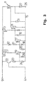
- circuit arrangement shown in FIG. 3 differs from that in FIG Figure 2 shown circuit arrangement essentially only by the placement of the current mirror. By shifting the current mirror behind the bipolar transistor 22 is here in contrast to that shown in Figure 2 Switching no quiescent current required.
- Figure 4 illustrates that the circuit arrangement shown in Figure 2 is not is only suitable for monitoring the chip-internal ground line 4, but can also be used to monitor other lines 32. This could e.g. the connection shown in dashed lines in Figure 1 to a lamp driver 8, which is identified in Figure 1 with 7.
- the exemplary embodiments discussed above show that with the Circuit proposed according to the invention in addition to that of the system logic implemented shutdown path an additional system logic independent Switch-off option for a MOSFET output stage is available.
- This additional switch-off option should only be used if critical on a line monitored by a detection logic Potentials arise.
- the detection logic ensures a quick shutdown the MOSFET output stage.
- the detection logic can be designed in this way be that a delay in the release of the MOSFET output stage after a shutdown is realized by the detection logic. This rectifier effect the detection logic prevents active operation of the MOSFET output stage, if oscillating potentials occur on the monitored line.
- the detection logic can be designed so that its shutdown function for the MOSFET power amplifier is overridden if Overvoltage pulses occur on the supply lines.
Landscapes
- Electronic Switches (AREA)
- Semiconductor Integrated Circuits (AREA)
- Logic Circuits (AREA)
- Metal-Oxide And Bipolar Metal-Oxide Semiconductor Integrated Circuits (AREA)
- Amplifiers (AREA)
Description
- Fig. 1
- den prinzipiellen Aufbau einer erfindungsgemäßen Schaltung zum Abschalten einer MOSFET-Endstufe,
- Fig. 2
- ein Ausführungsbeispiel einer Detektionslogik, mit der die chipinterne Masseleitung überwacht wird,
- Fig. 3
- ein weiteres Ausführungsbeispiel einer Detektionslogik, mit der die chipinteme Masseleitung überwacht wird, und
- Fig. 4
- ein Ausführungsbeispiel einer Detektionslogik, mit der ein anderes Signal überwacht wird.
Claims (10)
- Schaltung zum Abschalten einer MOSFET-Endstufe (1), insbesondere eines High-Side-PowerMos, beim Auftreten anormaler Potentiale auf mindestens einer überwachten Leitung, wobei mindestens eine Einrichtung (2) zum Steuern der MOSFET-Endstufe (1), insbesondere eine Ansteuerlogik mit einer Schutzschaltung gegen Übertemperatur und/oder Überlastung, und mindestens eine weitere Einrichtung (3) zum Überwachen der Leitung vorgesehen sind, wobei die MOSFET-Endstufe (1) unabhängig von der mindestens einen Einrichtung (2) zum Steuern der MOSFET-Endstufe (1) auch über die mindestens eine weitere Einrichtung (3) zum Überwachen der Leitung ausschaltbar ist, wobei die Leitung eine elektrische Verbindung zwischen einem Pol der Versorgungsspannung der Einrichtung (2), insbesondere chipinternem Massepotential oder Versorgungsspannungspotential, und der mindestens einen Einrichtung (2) bildet und durch die mindestens eine weitere Einrichtung (3) die Schaltung vor Fehlfunktionen der mindestens einen Einrichtung (2) geschützt wird, wobei
die weitere Einrichtung (3) zum Überwachen der mindestens einen Leitung (4) Mittel zum Vergleichen des Potentials der überwachten Leitung (4) mit einem Vergleichspotential umfaßt und die weitere Einrichtung (3) zum Überwachen der Leitung (4) die MOSFET-Endstufe (1) ausschaltet, wenn die Abweichung zwischen dem Potential der überwachten Leitung (4) und dem Vergleichspotential ein vorbestimmtes Maß überschreitet, dadurch gekennzeicknet, daß
die Mittel zum Überwachen der mindestens
einen Leitung (4, 32) mindestens einen Bipolartransistor (22) umfassen und der Basisanschluß des Bipolartransistors (22) mit der überwachten Leitung (4, 32) verbunden ist und der Emitter des Bipolartransistors (22) über mindestens einen elektrischen Widerstand (23, 24) mit dem Vergleichspotential verbunden ist. - Schaltung nach Anspruch 1, dadurch gekennzeichnet, daß die MOSFET-Endstufe (1) über die weitere Einrichtung (3) zum Überwachen der Leitung (4) ausgeschaltet wird, indem Gate und Source der MOSFET-Endstufe (1) kurzgeschlossen werden (Abschaltpfad II).
- Schaltung nach einem der Ansprüche 1 bis 2, dadurch gekennzeichnet, daß die weitere Einrichtung (3) zum Überwachen der mindestens einen Leitung (4) Mittel umfassen, mit denen das Wiedereinschalten der MOSFET-Endstufe (1) nach einem Ausschalten durch die weitere Einrichtung (3) zum Überwachen der Leitung (4) verzögert wird.
- Schaltung nach einem der Ansprüche 1 bis 3, dadurch gekennzeichnet, daß die weitere Einrichtung (3) zum Überwachen der mindestens einen Leitung (4) Mittel zum Überwachen des Stroms zwischen der überwachten Leitung (4) und einem definierten Potential umfassen und daß die weitere Einrichtung (3) zum Überwachen der Leitung (4) die MOSFET-Endstufe (1) ausschaltet, wenn der Strom einen vorbestimmten Wert über- bzw. unterschreitet.
- Schaltung nach einem der Ansprüche 1 bis 4, dadurch gekennzeichnet, daß die weitere Einrichtung (3) zum Überwachen der mindestens einen Leitung (4) Mittel umfaßt zum Außerkraftsetzen der Ausschaltfunktion für die MOSFET-Endstufe (1) beim Auftreten von Überspannungen.
- Schaltung nach einem der Ansprüche 1 bis 5, dadurch gekennzeichnet, daß die Mittel zum Überwachen der mindestens einen Leitung (4) einen ersten MOSFET (21) umfassen, über den Gate und Source der MOSFET-Endstufe (1) kurzschließbar sind.
- Schaltung nach einem der Ansprüche 1 bis 6, wobei mehrere Leitungen überwacht werden, dadurch gekennzeichnet, daß die Mittel zum Überwachen jeder Leitung mindestens einen Bipolartransistor umfassen und daß die Bipolartransistoren parallel geschaltet sind.
- Schaltung nach einem der Ansprüche 1 bis 7, dadurch gekennzeichnet, daß der Emitteranschluß des Bipolartransistors (22) über eine Spannungsteileranordnung (23, 24, 25) mit einem zweiten MOSFET (17) verbunden ist, wobei der Schaltzustand des zweiten MOSFET (17) den Schaltzustand des ersten MOSFET (21) beeinflußt, und daß die Spannungsteileranordnung (23, 24, 25) so dimensioniert ist, daß der zweite MOSFET (17) schnell einschaltbar aber nur verzögert ausschaltbar ist.
- Schaltung nach Anspruch 8, dadurch gekennzeichnet, daß zwischen der überwachtend Leitung (4, 32) und einem definierten Potential ein dritter MOSFET (10) angeordnet ist, wobei der Schaltzustand des dritten MOSFET (10) vom Strom zwischen der überwachten Leitung (4, 32) und dem definierten Potential abhängig ist und den Schaltzustand des ersten MOSFET (21) beeinflußt.
- Verwendung einer Schaltung nach einem der Ansprüche 1 bis 11 zur Überwachung einer chipinternen Masseleitung (4).
Applications Claiming Priority (3)
| Application Number | Priority Date | Filing Date | Title |
|---|---|---|---|
| DE19735541 | 1997-08-16 | ||
| DE19735541A DE19735541A1 (de) | 1997-08-16 | 1997-08-16 | Schaltung zum Abschalten einer MOSFET-Endstufe |
| PCT/DE1998/002131 WO1999009651A2 (de) | 1997-08-16 | 1998-07-28 | Schaltung zum abschalten einer mosfet-endstufe |
Publications (2)
| Publication Number | Publication Date |
|---|---|
| EP1072093A1 EP1072093A1 (de) | 2001-01-31 |
| EP1072093B1 true EP1072093B1 (de) | 2002-05-08 |
Family
ID=7839161
Family Applications (1)
| Application Number | Title | Priority Date | Filing Date |
|---|---|---|---|
| EP98947355A Expired - Lifetime EP1072093B1 (de) | 1997-08-16 | 1998-07-28 | Schaltung zum abschalten einer mosfet-endstufe |
Country Status (4)
| Country | Link |
|---|---|
| EP (1) | EP1072093B1 (de) |
| AU (1) | AU9431298A (de) |
| DE (2) | DE19735541A1 (de) |
| WO (1) | WO1999009651A2 (de) |
Families Citing this family (1)
| Publication number | Priority date | Publication date | Assignee | Title |
|---|---|---|---|---|
| DE10356089B4 (de) * | 2003-12-01 | 2005-11-03 | Siemens Ag | Schaltungsanordnung und Verfahren zum Steuern eines induktiven Verbrauchers |
Family Cites Families (6)
| Publication number | Priority date | Publication date | Assignee | Title |
|---|---|---|---|---|
| DE3539646C2 (de) * | 1985-11-08 | 1994-02-17 | Asea Brown Boveri | Schaltungsanordnung zum Schutz gegen Überlast |
| DE4142666C2 (de) * | 1991-12-21 | 1996-02-08 | Vdo Schindling | Schaltungsanordnung mit einem Halbleiterschalter zum Schalten einer Last |
| US5245526A (en) * | 1992-02-07 | 1993-09-14 | Power Integrations, Inc. | Below ground current sensing with current input to control threshold |
| DE4236334A1 (de) * | 1992-10-28 | 1994-05-05 | Bosch Gmbh Robert | Monolithisch integriertes MOS-Endstufenbauteil mit einer Überlast-Schutzeinrichtung |
| US5418673A (en) * | 1992-12-14 | 1995-05-23 | North American Philips Corporation | Control electrode disable circuit for power transistor |
| JP3982842B2 (ja) * | 1993-08-18 | 2007-09-26 | 株式会社ルネサステクノロジ | 半導体装置 |
-
1997
- 1997-08-16 DE DE19735541A patent/DE19735541A1/de not_active Ceased
-
1998
- 1998-07-28 WO PCT/DE1998/002131 patent/WO1999009651A2/de not_active Ceased
- 1998-07-28 DE DE59804103T patent/DE59804103D1/de not_active Expired - Lifetime
- 1998-07-28 AU AU94312/98A patent/AU9431298A/en not_active Abandoned
- 1998-07-28 EP EP98947355A patent/EP1072093B1/de not_active Expired - Lifetime
Also Published As
| Publication number | Publication date |
|---|---|
| EP1072093A1 (de) | 2001-01-31 |
| WO1999009651A3 (de) | 2000-12-07 |
| WO1999009651A2 (de) | 1999-02-25 |
| AU9431298A (en) | 1999-03-08 |
| DE59804103D1 (de) | 2002-06-13 |
| DE19735541A1 (de) | 1999-02-18 |
Similar Documents
| Publication | Publication Date | Title |
|---|---|---|
| DE4402095C2 (de) | Elektrostatische Entladeschutzschaltung mit dynamischer Triggerung | |
| DE10158790B4 (de) | Halbleiterschutzschaltung | |
| DE69011189T2 (de) | Treiber für Hochvolt-Halbbrücken-Schaltkreise. | |
| DE69221771T2 (de) | Leistungs-MOS-Einrichtung mit Schutzschaltung gegen Überstrom | |
| DE102005039371B4 (de) | Halbleitervorrichtung | |
| DE10344572A1 (de) | Gateansteuerungseinrichtung zur Reduktion einer Stoßspannung und einem Schaltverlust | |
| WO2009027348A2 (de) | Schaltungsanordnung zum schutz vor elektrostatischen entladungen und verfahren zum betreiben einer solchen | |
| DE10005864A1 (de) | Stromversorgungssteuereinheit und Stromversorgungssteuerverfahren | |
| DE19600808A1 (de) | Überspannungsklemmen- und Entsättigungsdetektionsschaltkreis | |
| EP0043489A1 (de) | Schalter mit in Serie geschalteten MOS-FET | |
| DE112013004659T5 (de) | Halbleiteransteuerungsvorrichtung | |
| DE69329484T2 (de) | Steuerelektroden-Abschaltkreis für einen Leistungstransistor | |
| DE112018003410T5 (de) | Kurzschlussschutzschaltung für ein Halbleiterschaltelement | |
| WO2021176003A1 (de) | Treiberschaltung für ein niederinduktives leistungsmodul sowie ein niederinduktives leistungsmodul mit erhöhter kurzschlussfestigkeit | |
| DE68924107T2 (de) | Steuerschaltung für die Begrenzungsspannung einer durch eine Leistungsvorrichtung in spannungsseitiger Treiberkonfiguration getriebenen induktiven Last. | |
| DE60309675T2 (de) | Leistungsschaltkreis mit gesteuertem Sperrstrom | |
| EP0384937A1 (de) | Schutzschaltung für einen Leistungs-MOSFET | |
| EP0361211B1 (de) | Schutzschaltung für einen Leistungshalbleiterbaustein | |
| EP0013710A1 (de) | Gegentakt-Treiberschaltung, deren Ausgang direkt mit den Ausgängen weiterer Treiberschaltungen verknüpfbar ist | |
| WO2011101356A1 (de) | Überspannungsschutz für einen halbleiterschalter | |
| DE102006021847B4 (de) | Schaltungsanordnung zum Schutz vor elektrostatischen Entladungen | |
| EP0393224B1 (de) | Schaltungsanordnung zur Temperaturüberwachung von in einem Halbleiterschaltkreis integrierten Leistungsschalttransistoren | |
| DE102009007818A1 (de) | Schaltungsanordnung mit einer Schaltbrücke aus NMOS-Transistoren und mit einer Verpolschutzeinrichtung | |
| EP4254797A2 (de) | Vorrichtung und verfahren zur verhinderung eines substratstroms in einem ic-halbleitersubstrat | |
| DE10211099B4 (de) | Vorrichtung zur Ansteuerung einer elektrischen Last |
Legal Events
| Date | Code | Title | Description |
|---|---|---|---|
| PUAI | Public reference made under article 153(3) epc to a published international application that has entered the european phase |
Free format text: ORIGINAL CODE: 0009012 |
|
| 17P | Request for examination filed |
Effective date: 20000316 |
|
| AK | Designated contracting states |
Kind code of ref document: A1 Designated state(s): DE FR IT |
|
| GRAG | Despatch of communication of intention to grant |
Free format text: ORIGINAL CODE: EPIDOS AGRA |
|
| 17Q | First examination report despatched |
Effective date: 20010724 |
|
| GRAG | Despatch of communication of intention to grant |
Free format text: ORIGINAL CODE: EPIDOS AGRA |
|
| GRAH | Despatch of communication of intention to grant a patent |
Free format text: ORIGINAL CODE: EPIDOS IGRA |
|
| GRAH | Despatch of communication of intention to grant a patent |
Free format text: ORIGINAL CODE: EPIDOS IGRA |
|
| GRAA | (expected) grant |
Free format text: ORIGINAL CODE: 0009210 |
|
| AK | Designated contracting states |
Kind code of ref document: B1 Designated state(s): DE FR IT |
|
| REF | Corresponds to: |
Ref document number: 59804103 Country of ref document: DE Date of ref document: 20020613 |
|
| ET | Fr: translation filed | ||
| PLBE | No opposition filed within time limit |
Free format text: ORIGINAL CODE: 0009261 |
|
| STAA | Information on the status of an ep patent application or granted ep patent |
Free format text: STATUS: NO OPPOSITION FILED WITHIN TIME LIMIT |
|
| 26N | No opposition filed |
Effective date: 20030211 |
|
| PGFP | Annual fee paid to national office [announced via postgrant information from national office to epo] |
Ref country code: FR Payment date: 20070718 Year of fee payment: 10 |
|
| REG | Reference to a national code |
Ref country code: FR Ref legal event code: ST Effective date: 20090331 |
|
| PG25 | Lapsed in a contracting state [announced via postgrant information from national office to epo] |
Ref country code: FR Free format text: LAPSE BECAUSE OF NON-PAYMENT OF DUE FEES Effective date: 20080731 |
|
| PGFP | Annual fee paid to national office [announced via postgrant information from national office to epo] |
Ref country code: IT Payment date: 20090728 Year of fee payment: 12 |
|
| PGFP | Annual fee paid to national office [announced via postgrant information from national office to epo] |
Ref country code: DE Payment date: 20100924 Year of fee payment: 13 |
|
| PG25 | Lapsed in a contracting state [announced via postgrant information from national office to epo] |
Ref country code: IT Free format text: LAPSE BECAUSE OF NON-PAYMENT OF DUE FEES Effective date: 20100728 |
|
| PG25 | Lapsed in a contracting state [announced via postgrant information from national office to epo] |
Ref country code: DE Free format text: LAPSE BECAUSE OF NON-PAYMENT OF DUE FEES Effective date: 20130201 |
|
| REG | Reference to a national code |
Ref country code: DE Ref legal event code: R119 Ref document number: 59804103 Country of ref document: DE Effective date: 20130201 |