EP1069682B1 - Circuit tampon commutable - Google Patents
Circuit tampon commutable Download PDFInfo
- Publication number
- EP1069682B1 EP1069682B1 EP00305781A EP00305781A EP1069682B1 EP 1069682 B1 EP1069682 B1 EP 1069682B1 EP 00305781 A EP00305781 A EP 00305781A EP 00305781 A EP00305781 A EP 00305781A EP 1069682 B1 EP1069682 B1 EP 1069682B1
- Authority
- EP
- European Patent Office
- Prior art keywords
- frequency
- circuit
- signal
- supplied
- oscillator
- Prior art date
- Legal status (The legal status is an assumption and is not a legal conclusion. Google has not performed a legal analysis and makes no representation as to the accuracy of the status listed.)
- Expired - Lifetime
Links
Images


Classifications
-
- H—ELECTRICITY
- H03—ELECTRONIC CIRCUITRY
- H03J—TUNING RESONANT CIRCUITS; SELECTING RESONANT CIRCUITS
- H03J5/00—Discontinuous tuning; Selecting predetermined frequencies; Selecting frequency bands with or without continuous tuning in one or more of the bands, e.g. push-button tuning, turret tuner
- H03J5/24—Discontinuous tuning; Selecting predetermined frequencies; Selecting frequency bands with or without continuous tuning in one or more of the bands, e.g. push-button tuning, turret tuner with a number of separate pretuned tuning circuits or separate tuning elements selectively brought into circuit, e.g. for waveband selection or for television channel selection
- H03J5/242—Discontinuous tuning; Selecting predetermined frequencies; Selecting frequency bands with or without continuous tuning in one or more of the bands, e.g. push-button tuning, turret tuner with a number of separate pretuned tuning circuits or separate tuning elements selectively brought into circuit, e.g. for waveband selection or for television channel selection used exclusively for band selection
- H03J5/244—Discontinuous tuning; Selecting predetermined frequencies; Selecting frequency bands with or without continuous tuning in one or more of the bands, e.g. push-button tuning, turret tuner with a number of separate pretuned tuning circuits or separate tuning elements selectively brought into circuit, e.g. for waveband selection or for television channel selection used exclusively for band selection using electronic means
-
- H—ELECTRICITY
- H03—ELECTRONIC CIRCUITRY
- H03B—GENERATION OF OSCILLATIONS, DIRECTLY OR BY FREQUENCY-CHANGING, BY CIRCUITS EMPLOYING ACTIVE ELEMENTS WHICH OPERATE IN A NON-SWITCHING MANNER; GENERATION OF NOISE BY SUCH CIRCUITS
- H03B5/00—Generation of oscillations using amplifier with regenerative feedback from output to input
- H03B5/08—Generation of oscillations using amplifier with regenerative feedback from output to input with frequency-determining element comprising lumped inductance and capacitance
- H03B5/12—Generation of oscillations using amplifier with regenerative feedback from output to input with frequency-determining element comprising lumped inductance and capacitance active element in amplifier being semiconductor device
- H03B5/1231—Generation of oscillations using amplifier with regenerative feedback from output to input with frequency-determining element comprising lumped inductance and capacitance active element in amplifier being semiconductor device the amplifier comprising one or more bipolar transistors
-
- H—ELECTRICITY
- H03—ELECTRONIC CIRCUITRY
- H03K—PULSE TECHNIQUE
- H03K5/00—Manipulating of pulses not covered by one of the other main groups of this subclass
- H03K5/00006—Changing the frequency
-
- H—ELECTRICITY
- H03—ELECTRONIC CIRCUITRY
- H03L—AUTOMATIC CONTROL, STARTING, SYNCHRONISATION OR STABILISATION OF GENERATORS OF ELECTRONIC OSCILLATIONS OR PULSES
- H03L7/00—Automatic control of frequency or phase; Synchronisation
- H03L7/06—Automatic control of frequency or phase; Synchronisation using a reference signal applied to a frequency- or phase-locked loop
- H03L7/08—Details of the phase-locked loop
- H03L7/099—Details of the phase-locked loop concerning mainly the controlled oscillator of the loop
Definitions
- the present invention relates to a frequency characteristic switchable buffer circuit, and more particularly, to a frequency characteristic switchable buffer circuit for outputting a selected frequency signal component in a state in which a not selected frequency signal component is sufficiently attenuated by providing signals of a first frequency and a second frequency, which are selectively supplied, with excellent frequency selecting characteristics, respectively.
- DCS digital cellular system
- GSM global system for mobile communications
- DCS is a mobile communication system in which frequencies of 1805 MHz to 1880 MHz are allocated as a base station frequency, frequencies of 1710 MHz to 1785 MHz are allocated as a mobile station frequency, a 1700 MHz band is allocated as oscillation frequencies of a voltage-controlled oscillator (VCO) of portable telephone sets, 374 channels are used, and a Gaussian minimum shift keying (GMSK) is used as a modulation system.
- VCO voltage-controlled oscillator
- GMSK Gaussian minimum shift keying
- GSM Global System for Mobile communications
- GSM Global System for Mobile communications
- frequencies of 925 MHz to 960 MHz are allocated as a base station frequency
- frequencies of 880 MHz to 915 MHz are allocated as a mobile station frequency
- a 900 MHz band is allocated as oscillation frequencies of a voltage-controlled oscillator (VCO) of portable telephone sets
- 124 channels are used
- the Gaussian minimum shift keying (GMSK) is used as a modulation system.
- a receiver with a buffer in which a parallel resonant circuit at the output and a low-pass filter at the input are switched to operate in two frequency bands is known from the document US-5-758-276.
- Both DCS and GSM employ GMSK as the modulation system thereof and are different from each other only in that they use different frequencies allocated thereto.
- GMSK modulation system
- This portable telephone set is provided with a switching type oscillator which includes two voltage-controlled oscillators, that is, a first voltage-controlled oscillator for oscillating a first frequency of the 1700 MHz band, a second voltage-controlled oscillator for oscillating a second frequency of the 900 MHz band and a switching circuit so that the portable telephone set can separately use the two voltage-controlled oscillators by controlling the switching circuit of the switching type oscillator.
- the portable telephone set which can be used in both of DCS and GSM, carries out mobile communication through DCS
- the first voltage-controlled oscillator is switched to an operating state and the second voltage-controlled oscillator is switched to a non-operating state by the switching circuit and an oscillation signal of a first frequency is output from the first voltage-controlled oscillator.
- the portable telephone set which can be used in both of DCS and GSM
- the second voltage-controlled oscillator is switched to an operating state and the first voltage-controlled oscillator is switched to a non-operating state by the switching circuit and an oscillation signal of a second frequency is output from the second voltage-controlled oscillator.
- the oscillation signal of the first frequency and the oscillation signal of the second frequency are selectively amplified by a frequency characteristic switchable buffer circuit and then supplied to a circuit where it is used.
- the frequency characteristic switchable buffer circuit which is used at that time includes a parallel resonant circuit (frequency selection circuit).
- a parallel resonant circuit frequency selection circuit.
- a first switching voltage or a second switching voltage is supplied to the parallel resonant circuit so that the frequency selecting characteristics thereof are switched.
- the first switching voltage is supplied to the parallel resonant circuit, it selects the oscillation signal of the first frequency and causes the first voltage-controlled oscillator to output it
- the second switching voltage is supplied to the parallel resonant circuit, it selects the oscillation signal of the second frequency and causes the second voltage-controlled oscillator to output it.
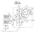
- Fig. 6 is a circuit diagram showing an example of an arrangement of a conventional frequency characteristic switchable buffer circuit which is used in a portable telephone set which is can be used in both of DCS and GSM.
- the conventional frequency characteristic switchable buffer circuit 50 includes a transistor 51, a parallel resonant circuit (frequency selection circuit) 52, coupling capacitors 53 and 54, base bias resistors 55 and 56, an emitter resistor 57, a bypass capacitor 58, a one-circuit two-contacts changeover switch 59, a switching voltage setting resistors 60 and 61, a bypass capacitor 62, a buffer resistor 63, a signal input terminal 64, a signal output terminal 65, and a power supply terminal 66.
- These circuit elements 51 to 66 are connected as shown in Fig. 6.
- the parallel resonant circuit 52 is composed of a first inductor 52 1 , a second inductor 52 2 , a first capacitor 52 3 , a second capacitor 52 4 , a third capacitor 52 5 , and a switching diode 52 6 , and these circuit elements 52 1 to 52 6 are connected as shown in Fig. 6.
- a first voltage-controlled oscillator 67 for oscillating a first frequency in this case, a frequency of a 1700 MHz band
- a second voltage-controlled oscillator 68 for oscillating a second frequency in this case, a frequency of a 900 MHz band
- a power supply 69 disposed in the former stage of the frequency characteristic switchable buffer circuit 50.
- These circuit elements 67 to 70 are connected as shown in Fig. 6.
- the changeover switches 59 and 70 are switched in association with each other in response to a control signal which will be described later.
- the conventional frequency characteristic switchable buffer circuit 50 arranged as described above will operate as described below.
- the respective movable contacts of the changeover switches 59 and 70 are switched from the positions shown by solid lines to the positions shown by dotted lines shown in Fig. 6 in response to a first control signal supplied from a controller (not shown).
- a controller not shown
- the first voltage-controlled oscillator 67 is connected to the power supply 69 and put into an operating state and a signal of the first frequency (frequency of the 1700 MHz band) is supplied from the first voltage-controlled oscillator 67, whereas the second voltage-controlled oscillator 68 is isolated from the power supply 69 and put into a non-operating state.
- a first positive switching voltage is supplied to the parallel resonant circuit 52 so that the parallel resonant circuit 52 performs a parallel resonance at the first frequency (frequency of the 1700 MHz band) as described below.
- the signal of the first frequency (frequency of the 1700 MHz band) output from the first voltage-controlled oscillator 67 is supplied to the signal input terminal 64 and then is amplified by the emitter-grounded transistor 51, only the signal of the first frequency (frequency of the 1700 band) is selectively amplified by the parallel resonant circuit 52 which is connected to the transistor 51 as a load thereon and in parallel resonance with the first frequency (frequency of the 1700 MHz band). Then, the thus amplified signal of the first frequency (frequency of the 1700 band) is supplied from the signal output terminal 65 to the circuit where it is used.
- the respective movable contacts of the changeover switches 59 and 70 are switched to the positions shown by the solid lines in Fig. 6 in response to a second control signal supplied from the controller in the same manner.
- the second voltage-controlled oscillator 68 is connected to the power supply 69 and put into an operating state and a signal of the second frequency (frequency of the 900 MHz band) is supplied from the second voltage-controlled oscillator 68, whereas the first voltage-controlled oscillator 67 is isolated from the power supply 69 and put into a non-operating state.
- a second ground switching voltage is supplied to the parallel resonant circuit 52 so that the parallel resonant circuit 52 performs a parallel resonance at the second frequency (frequency of the 900 MHz band) as described below.
- the signal of the second frequency (frequency of the 900 MHz band) output from the second voltage-controlled oscillator 68 is supplied to the signal input terminal 64 and then amplified by the emitter-grounded transistor 51, only the signal of the second frequency (frequency of the 900 MHz band) is selectively amplified by the parallel resonant circuit 52 which is connected to the transistor 51 as a load thereon and in parallel resonance with the second frequency (frequency of the 900 MHz band). Then, the thus amplified signal of the second frequency (frequency of the 900 MHz band) is supplied from the signal output terminal 65 to the circuit where it is used.
- the switching diode 52 6 is turned off in response to the second ground switching voltage supplied to the parallel resonant circuit 52, whereby the connecting point where the second capacitor 52 4 is connected to the third capacitor 52 5 is isolated from ground.
- a parallel resonant frequency which is approximate equal to the second frequency (frequency of the 900 MHz band) is set to the parallel resonant circuit 52 by a first parallel connecting circuit, which is composed of the first inductor 52 1 and the first capacitor 52 3 , and by a second parallel connecting circuit, which is composed of the second inductor 52 2 which is connected in series to the first parallel connecting circuit and of the second capacitor 52 4 and the third capacitor 52 5 which are connected in series to the first parallel connecting circuit.
- the second parallel connecting circuit exhibits a minute capacitor at the second frequency (frequency of the 900 MHz band) and the parallel resonant circuit 52 is arranged as an equivalent circuit which is composed of a series circuit including the first inductor 52 1 and the minute capacitor and of the first capacitor 52 3 connected in parallel to the first inductor 52 1 , whereby a parallel resonant frequency of the parallel resonant circuit 52 can easily be set to the second frequency (frequency of the 900 MHz band).
- the parallel resonant circuit 52 when the parallel resonant circuit 52 is caused to perform a parallel resonance with the signal of the first frequency (frequency of the 1700 MHz band) by supplying the first positive switching voltage to the parallel resonant circuit 52, the switching diode 52 6 is turned on in response to the first positive switching voltage supplied to the parallel resonant circuit 52, whereby the connecting point where the second capacitor 52 4 is connected to the third capacitor 52 5 is connected to ground.
- a parallel resonant frequency which is approximate equal to the first frequency (frequency of the 1700 MHz band) is set to the parallel resonant circuit 52 by the second inductor 52 2 and by the second capacitor 52 4 and the third capacitor 52 5 which are connected in parallel to the second inductor 52 2 .
- the parallel connecting circuit including the second capacitor 52 4 and the third capacitor 52 5 exhibit a synthetic capacitor and the parallel resonant circuit 52 is arranged as an equivalent capacitor composed of the second inductor 52 2 and the synthetic capacitor which are connected thereto in parallel therewith. Accordingly, a parallel resonant frequency of the parallel resonant circuit 52 can be easily set to the first frequency (frequency of the 1700 MHz band)
- Fig. 7 is a characteristic view showing an example of characteristics between gain and frequency in the conventional frequency characteristic switchable buffer circuit 50 shown in Fig. 6.
- Fig. 7 the abscissa shows frequency (unit: GHz) and the ordinate shows gain (unit: dB).
- a curve (solid line) a shows characteristics when the buffer circuit 50 performs a parallel resonance at the first frequency of the 1.7 GHz (1700 MHz band), whereas a curve b shows characteristics when the buffer circuit 50 is tuned for the second frequency of the 0.9 GHz (900 MHz band).
- the buffer circuit 50 when the signal of the first frequency (frequency of the 1700 MHz band) is selected as an amplifying signal, the buffer circuit 50 has a large gain with respect to the signal of the first frequency, whereas when the signal of the second frequency (frequency of the 1700 MHz band) is selected as the amplifying signal, the buffer circuit 50 has a large gain with respect to the signal of the second frequency.
- the buffer circuit 50 can take out the signal of the first frequency which has a large signal amplitude.
- the signal of the second frequency frequency of 900 MHz band
- the buffer circuit 50 can take out the signal of the second frequency which has a large signal amplitude in the same manner.
- the conventional frequency characteristic switchable buffer circuit 50 cannot obtain a so large amount of attenuation with respect to a signal on the side of a frequency which is higher than the first frequency. Accordingly, there is an increased possibility that a signal of a frequency which is spurious to the first frequency is output simultaneously with the output of the signal of the first frequency. Further, when the signal of the second frequency (frequency of 900 MHz band) is selected, the buffer circuit 50 cannot obtain a so large amount of attenuation of the harmonics component of the signal of the second frequency. Accordingly, there is an increased possibility that a signal of a spurious frequency is output simultaneously with the output of the signal of the second frequency.
- An object of the present invention which was made in view of the above technological background, is to provide a frequency characteristic switchable buffer circuit capable of increasing an amount of attenuation of a signal of a spurious frequency when a signal of a first frequency is selected and capable of increasing an amount of attenuation of a signal of a spurious frequency when a signal of a second frequency is selected.
- a frequency characteristic switchable buffer circuit of the present invention has a first arrangement in which the buffer circuit includes an amplifier stage, a parallel resonant circuit which acts as an output load on the amplifier stage, a frequency trap circuit connected between the input of the amplifier stage and a reference potential, and a frequency switching voltage generator for selectively generating a first switching voltage and a second switching voltage, wherein the parallel resonant circuit performs a parallel resonance at a first frequency when the first switching voltage is supplied and performs a parallel resonance at a second frequency which is different from the first frequency when the second switching voltage is supplied, the frequency trap circuit is composed of a series circuit including a diode and a capacitor and performs a series resonance at the second frequency when the first switching voltage is supplied and performs a series resonance at the first frequency when the second switching voltage is supplied.
- the first switching voltage is supplied to the parallel resonant circuit, and the parallel resonant circuit is caused to perform a parallel resonance at the first frequency so as to selectively output a signal of the first frequency.
- the first switching voltage is supplied also to the frequency trap circuit so that the frequency trap circuit is caused to perform a series resonance at a frequency which is lower than the first frequency so as to form a trap to the low frequency as well as when a trap is generated to the side of a frequency which is higher than the first frequency by the rebound of the formation of the above trap, the signal component of the spurious frequency of the signal of the first frequency is attenuated by these traps.
- the second switching voltage is supplied to the parallel resonant circuit, the parallel resonant circuit is caused to perform a parallel resonance at the second frequency so as to selectively output a signal of the second frequency.
- the second switching voltage is supplied also to the frequency trap circuit so that the frequency trap circuit is caused to perform a series resonance at a frequency in the vicinity of 1700 MHz so as to generate a trap to the frequency in the vicinity of 1700 MHz
- the signal component of the spurious frequency of the second frequency signal is attenuated by the trap.
- an amount of attenuation of the signal component of the spurious frequency of the signal of the first frequency can be increased.
- an inductor is connected in series to the series circuit including the diode and the capacitor and in which an additional capacitor is connected in parallel to the diode.
- the frequency trap circuit When the first switching voltage is supplied to the frequency trap circuit so as to make the diode conductive as well as when the frequency trap circuit is caused to perform a series resonance at a frequency in the vicinity of 900 MHz through the capacitor and the diode by adjusting a capacitance value of the capacitor and an inductance value of the inductor, not only the signal component of the spurious frequency of the first frequency is attenuated but also a trap is generated on the side of a frequency which is higher than the first frequency by the rebound of the attenuation, and the thus generated trap attenuates the signal component of the spurious frequency of the first frequency.
- an amount of attenuation of the signal of the spurious frequency of the signal of the second frequency can be greatly increased as compared with an amount of attenuation of the signal in the first arrangement, whereby the first frequency signal and the second frequency signal in which almost no spurious signal component is contained can be selectively output.
- the first frequency be supplied from a first oscillator and the second frequency be supplied from a second oscillator, the first oscillator and the second oscillator be alternately switched to an operating state and to a non-operating state, and when the first oscillator is in the operating state, the frequency switching voltage generator be switched to generate the first switching voltage, and when the second oscillator is in the operating state, the frequency switching voltage generator be switched to generate the second switching voltage.
- the first oscillator since the first oscillator generates the first frequency and the second oscillator generates the second frequency, it is possible to set the first frequency and the second frequency in an arbitrary frequency range. As a result, a range of a technology, to which the frequency characteristic switchable buffer circuit is applied, can be increased.
- the second frequency and the first frequency have a relationship of a basic wave frequency and its harmonic frequency
- the second frequency is directly supplied from an oscillator and the first frequency is supplied from a harmonic oscillator to which the second frequency is imposed
- the frequency switching voltage generator is switched to output the first switching voltage
- the frequency switching voltage generator is switched to output the second switching voltage
- the first frequency and the second frequency can be selectively supplied to the frequency characteristic switchable buffer circuit only by a single oscillator, whereby a manufacturing cost can be reduced.
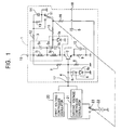
- Fig. 1 is a circuit arrangement diagram showing a first embodiment of a frequency characteristic switchable buffer circuit wherein shown is an example in which the buffer circuit is used in a portable telephone set which can be used in both of DCS and GSM.
- the frequency characteristic switchable buffer circuit 1 of the first embodiment includes a transistor 2, a parallel resonant circuit (frequency selection circuit) 3, coupling capacitors 4 and 5, a frequency trap circuit 6, base bias resistors 7 and 8, an emitter resistor 9, a bypass capacitor 10, a one-circuit two-contacts changeover switch 11, a switching voltage setting resistors 12 and 13, a bypass capacitor 14, buffer resistors 15 and 16, a signal input terminal 17, a signal output terminal 18, and a power supply terminal 19.
- These circuit elements 1 to 19 are connected as shown in Fig. 1.
- the parallel resonant circuit 3 includes a first inductor 3 1 , a second inductor 3 2 , a first capacitor 3 3 , a second capacitor 3 4 , a third capacitor 3 5 , and a first switching diode 3 6 .
- the frequency trap circuit 6 includes a fourth capacitor 6 1 , and a second switching diode 6 2 . These circuit elements 3 1 to 3 6 and 6 1 and 6 2 are connected as shown in Fig. 1.
- an inductance of the first inductor 3 1 is selected so that it is larger than an inductance of the second inductor 3 2 of the parallel resonant circuit 3.
- a capacitance of the third capacitor 3 5 is selected so that it is considerably larger than a capacitance of the second capacitor 3 4 , for example, so that the capacitance of the second capacitor 3 4 is set to about 2 pF when the capacitance of the third capacitor 3 5 is 1000 pF.
- a first voltage-controlled oscillator 20 for oscillating a first frequency in this case, a frequency of a 1700 MHz band
- a second voltage-controlled oscillator 21 for oscillating a second frequency in this case, a frequency of the 900 MHz band
- a power supply 22 disposed in the former stage of the frequency characteristic switchable buffer circuit 1 are a first voltage-controlled oscillator 20 for oscillating a first frequency, in this case, a frequency of a 1700 MHz band
- a second voltage-controlled oscillator 21 for oscillating a second frequency in this case, a frequency of the 900 MHz band
- a power supply 22 a one-circuit two-contacts changeover switch 23.
- These circuit elements 20 to 23 are connected as shown in Fig. 1. In this case, the changeover switches 11 and 23 are switched in association with each other in response to a control signal which will be described later.
- the frequency characteristic switchable buffer circuit 1 of the first embodiment (hereinafter, referred to as the buffer circuit 1 of the first embodiment) is arranged similarly to the conventional frequency characteristic switchable buffer circuit 50 shown in Fig. 6 (hereinafter, referred to as the conventional buffer circuit 50) except the following arrangement. That is, the buffer circuit 1 of the first embodiment is provided with the frequency trap circuit 6 and selectively supplies a first switching voltage or a second switching voltage to the second switching diode 6 2 of the frequency trap circuit 6 in relation to the provision of the frequency trap circuit 6, whereas the conventional buffer circuit 50 is not provided with the frequency trap circuit 6.
- the parallel resonant circuit 3 of the buffer circuit 1 of the first embodiment is arranged similarly to the parallel resonant circuit 52 of the conventional buffer circuit 50.
- the operation which is performed when the first switching voltage or the second switching voltage is supplied to the parallel resonant circuit 3 of the buffer circuit 1 of the first embodiment is the same as operation performed when the first switching voltage or the second switching voltage is supplied to the parallel resonant circuit 52 of the conventional buffer circuit 50 which was described above.
- the description of the operation of the conventional buffer circuit 50 when the first switching voltage or the second switching voltage is supplied to the parallel resonant circuit 52 of the buffer circuit 50 will be invoked to the description of the operation of the buffer circuit 1 of the first embodiment, and the description of the operation of the buffer circuit 1 when the first switching voltage or the second switching voltage is supplied to the parallel resonant circuit 3 of the buffer circuit 1 is omitted.
- the frequency characteristic switchable buffer circuit 1 of the first embodiment arranged as described above will operate as described below.
- the respective movable contacts of the changeover switches 11 and 23 are switched from the positions shown by solid lines to the positions shown by dotted lines shown in Fig. 1 in response to a first control signal supplied from a controller (not shown).
- a controller not shown
- the first voltage-controlled oscillator 20 is connected to the power supply 22 and put into an operating state and a signal of the first frequency (frequency of the 1700 MHz band) is supplied from the first voltage-controlled oscillator 20, whereas the second voltage-controlled oscillator 21 is isolated from the power supply 69 and put into a non-operating state.
- a first positive switching voltage is supplied to the parallel resonant circuit 3 so that the parallel resonant circuit 3 performs a parallel resonance at the first frequency as described above.
- the first positive switching voltage is supplied to the frequency trap circuit 6 so that the frequency trap circuit 6 performs a series resonance at the second frequency (frequency of 900 MHz band as described below).
- the signal of the first frequency output from the first voltage-controlled oscillator 20 is supplied to the signal input terminal 17 and then amplified by the emitter-grounded transistor 2, only the signal of the first frequency is selectively amplified by the parallel resonant circuit 3 which is connected to the transistor 2 as a collector load thereof and performs a parallel resonance at the first frequency. Then, the thus amplified signal of the first frequency is supplied to a circuit where it is used through the signal output terminal 18. At that time, the frequency trap circuit 6, which performs a series resonance at a frequency (for example, frequency of the 900 MHz band) which is lower than the first frequency (frequency of the 1700 MHz band), is connected between the base of the transistor 2 and the ground.
- a frequency for example, frequency of the 900 MHz band
- the first frequency frequency of the 1700 MHz band
- the frequency trap circuit 6 when the frequency trap circuit 6 is caused to perform a series resonance at the low frequency (frequency of the 900 MHz band), a trap resulting from the rebound of the series resonance is generated on the side of a frequency which is higher than the first frequency (frequency of the 1700 MHz band), whereby the signal component of a spurious frequency contained in the signal of the first frequency is sufficiently attenuated.
- the signal output terminal 18 only the signal of the first frequency which does not contain the signal component of the spurious frequency can be supplied to the signal output terminal 18.
- the respective movable contacts of the changeover switches 11 and 23 are switched to the positions shown by the solid lines in Fig. 1 in response to a second control signal supplied from the controller in the same manner.
- the second voltage-controlled oscillator 21 is connected to the power supply 22 and put into an operating state and a signal of the second frequency (frequency of the 900 MHz band) is supplied from the second voltage-controlled oscillator 21, whereas the first voltage-controlled oscillator 20 is isolated from the power supply 22 and put into a non-operating state.
- a second ground switching voltage is supplied to the parallel resonant circuit 3 so that the parallel resonant circuit 3 performs a parallel resonance at the second frequency as described below.
- the second ground switching voltage is supplied to the frequency trap circuit 6 so that the frequency trap circuit 6 performs a series resonance at the frequency of the 1700 MHz band.
- the signal of the second frequency output from the second voltage-controlled oscillator 21 is supplied to the signal input terminal 17 and then amplified by the emitter-grounded transistor 2, only the signal of the second frequency is selectively amplified by the parallel resonant circuit 3 which is connected to the transistor 2 as a collector load thereof and performs a parallel resonance at the second frequency. Then, the thus amplified signal of the second frequency is supplied to the circuit where it is used through the signal output terminal 18.
- the frequency trap circuit 6, which performs a series resonance at the first frequency (frequency of the 1700 MHz band) is connected between the base of the transistor 2 and the ground, the spurious signal component contained in the signal of the second frequency is sufficiently attenuated by the frequency trap circuit 6. As a result, it is possible to supply only the signal of the second frequency which does not contain the spurious signal component.
- Figs. 2A and 2B show equivalent circuit diagrams when the first or second switching signal is supplied to the frequency trap circuit 6 shown in Fig. 1.
- the second switching diode 6 2 is turned on, whereby only the lead wire inductor 6 3 of the lead wire of the second switching diode 6 2 which acts as the second switching diode 6 2 remains as a circuit element and connected in series to the fourth capacitor 61.
- the frequency trap circuit 6 is arranged as a series circuit composed of the fourth capacitor 6 1 and the lead wire inductor 6 3 as shown in Fig. 2A.
- the series circuit when the series circuit is caused to perform a series resonance at a frequency (for example, frequency of the 900 MHz band) which is lower than the first frequency (frequency of the 1700 MHz band) by selecting a capacitance value of the fourth capacitor 6 1 and an inductance value of the lead wire inductor 6 3 , a trap is generated on the side of a frequency which is higher than the first frequency (frequency of the 1700 MHz band) by the rebound of the above resonance, and the thus generated trap greatly attenuates the spurious high-frequency signal component of the first frequency.
- a frequency for example, frequency of the 900 MHz band
- the first frequency frequency of the 1700 MHz band
- the second switching diode 6 2 is turned off, whereby a series circuit composed of the lead wire inductor 6 3 of the lead wire of the second switching diode 6 2 which acts as the second switching diode 6 2 and the junction capacitor 6 4 of the semiconductor junction of the lead wire inductor 6 3 remains as a circuit element and connected in series to the fourth capacitor 6 1 .
- the frequency trap circuit 6 is composed of the series circuit including the fourth capacitor 6 1 , the lead wire inductor 6 3 , and the junction capacitor 6 4 as shown in Fig. 2B.
- the series circuit is caused to perform a series resonance at the first frequency (frequency of 1700 MHz band) by selecting a capacitance value of the fourth capacitor 6 1 , an inductance value of the lead wire inductor 6 3 , and a capacitance value of the junction capacitor 6 4 , the spurious high-frequency signal component of the second frequency (frequency of the 900 MHz band) can be greatly attenuated.
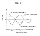
- Fig. 3 is a characteristic view showing characteristics between gain and frequency which can be obtained by the buffer circuit 1 of the first embodiment shown in Fig. 1.
- Fig. 3 the abscissa shows frequency (unit: GHz) and the ordinate shows gain (unit: dB).
- a curve (solid line) a shows characteristics when the parallel resonant circuit 3 of the buffer circuit 1 performs a parallel resonance at the first frequency of the 1.7 GHz band (frequency of the 1700 MHz band) and when a rebound trap is generated by the frequency trap circuit 6 on the side of a frequency which is higher than the first frequency (frequency of the 1700 MHz band).
- a curve (dotted line) b 1 shows characteristics when the parallel resonant circuit 3 of the buffer circuit 1 performs a parallel resonance at the second frequency of the 0.9 GHz band (frequency of the 900 MHz band) and when the frequency trap circuit 6 performs a parallel resonance at the frequency of the 1.7 GHz band (frequency of the 1700 MHz band).
- the buffer circuit 1 of the first embodiment not only can greatly increase an amount of attenuation of the signal component of the spurious frequency of the first frequency when the signal of the first frequency (frequency of the 1700 MHz band) is selected but also can greatly increase an amount of attenuation of the signal component of the frequency of the 1700 MHz band when the signal of the second frequency (frequency of the 900 MHz band) is selected. Therefore, the buffer circuit 1 can selectively output the signal of the first frequency and the signal of the second frequency in which almost no spurious signal component is contained.
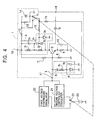
- Fig. 4 is a circuit arrangement diagram showing a second embodiment of the frequency characteristic switchable buffer circuit according to the present invention and shows an example in which a frequency trap circuit 6' is arranged differently from the frequency trap circuit 6 of the first embodiment.
- the second embodiment shows an example in which a buffer circuit is used in a portable telephone set which can be used in both of DCS and GSM similarly to the buffer circuit 1 of the first embodiment.
- the frequency trap circuit 6' in the buffer circuit 1 of the second embodiment includes a third inductor 6 5 and a fifth capacitor (added capacitor) 6 6 , in addition to the fourth capacitor 6 1 and the second switching diode 6 2 .
- the third inductor 6 5 is connected in series to the fourth capacitor 6 1 and the second switching diode 6 2
- the fifth capacitor 6 6 is connected in parallel to the second switching diode 6 2
- a first switching signal or a second switching signal is supplied to a node where the second switching diode 6 2 is connected to the third inductor 6 5 .
- the buffer circuit 1 of the second embodiment is arranged similarly to the buffer circuit 1 of the first embodiment except the frequency trap circuit 6'.
- the buffer circuit 1 of the second embodiment arranged as described above will operate as described below.
- the operation of the buffer circuit 1 of the second embodiment other than the frequency trap circuit 6' is the same as that of the buffer circuit 1 of the first embodiment, only the operation executed by the frequency trap circuit 6' will be described here, and the description of the operation of the components other than the frequency trap circuit 6' will be omitted.
- the second switching diode 6 2 is turned on, whereby only the lead wire indictor 6 3 of the lead wire of the second switching diode 6 2 which acts as the second switching diode 6 2 remains as a circuit element and is connected in series to the fourth capacitor 6 1 and the third inductor 6 5 . Note that since an inductance value of the lead wire inductor 6 3 is considerably smaller than an inductance value of the third inductor 6 5 , it may be ignored in this case.
- the frequency trap circuit 6' is arranged as a series circuit composed of the fourth capacitor 6 1 and the third inductor 6 5 . Accordingly, when the series circuit is caused to perform a series resonance at a frequency (for example, frequency of the 900 MHz band) which is lower than the first frequency (frequency of the 1700 MHz band) by selecting a capacitance value of the fourth capacitor 6 1 and an inductance value of the third inductor 6 5 , a frequency component of the 900 MHz band is trapped so that the frequency component of the 900 MHz band can be greatly attenuated as well as a trap also is generated on the side of a frequency which is higher than the first frequency (frequency of 1700 MHz band) by the rebound of the attenuation, and the thus generated trap can greatly attenuate the spurious high-frequency signal component of the first frequency.
- a frequency for example, frequency of the 900 MHz band
- the third inductor 6 5 a frequency component of the 900 MHz band is trapped so that the frequency component of the
- the second switching diode 62 is turned off, whereby a series circuit composed of the lead wire indictor 6 3 of the lead wire of the second switching diode 6 2 which acts as the second switching diode 6 2 and the junction capacitor 6 4 of the semiconductor junction of the lead wire indictor 6 3 remains as a circuit element and connected in series to the fourth capacitor 61 and the third inductor 6 5 .
- an inductance value of the lead wire inductor 6 3 is considerably smaller than that of the third inductor 65, it may be ignored in this case.
- a capacitance value of the junction capacitor 6 4 of the semiconductor junction is considerably smaller than that of the fifth capacitor 6 6 , it may be ignored in this case.
- the frequency trap circuit 6 is arranged as a series circuit including the fourth capacitor 6 1 , the third inductor 6 5 and the fifth capacitor 6 6 .
- the series circuit is caused to perform a series resonance at the first frequency (frequency of the 1700 MHz band) by selecting respective capacitance values of the fourth and fifth capacitors 6 1 and 6 6 and an inductance value of the third inductor 6 5 , the frequency component of the 1700 MHz band is trapped and a spurious high-frequency signal component of the second frequency (frequency of the 900 MHz band) can be greatly attenuated.
- the buffer circuit 1 of the second embodiment exhibits characteristics between gain and frequency as shown by a curve (dot-dash-line) b 2 of Fig. 3. That is, in the buffer circuit 1 of the second embodiment, a curve a , which shows characteristics between gain and frequency with respect to the first frequency, shows the same characteristics as those shown by the curve a of the buffer circuit 1 of the first embodiment, and the curves b 1 and b 2 , which show characteristics between gain and frequency with respect to the second frequency, show the same characteristics as those shown by the curve b 1 of the buffer circuit 1 of the first embodiment except the characteristics in the vicinity of the first frequency (frequency of the 1700 MHz band). More specifically, as to the characteristics in the vicinity of the first frequency (frequency of the 1700 MHz band), an amount of attenuation is greatly increased as shown by the curve b 2 as compared with that shown in the curve b 1 .
- the buffer circuit 1 of the second embodiment not only can greatly increase an amount of attenuation of the signal component of the spurious frequency of the first frequency when the signal of the first frequency (frequency of the 1700 MHz band) is selected but also can greatly increase an amount of attenuation of the signal component of the frequency of the 1700 MHz band as compared with the buffer circuit 1 of the first embodiment when the signal of the second frequency (frequency of the 900 MHz band) is selected. Therefore, the buffer circuit 1 can selectively output the signal of the first frequency and the signal of the second frequency in which almost no spurious signal component is contained.
- the frequency characteristic switchable buffer circuit 1 in the portable telephone set which can be used in both of DCS and GSM, an oscillation signal output from the first voltage-controlled oscillator 20 has a frequency of the 1700 MHz band, and an oscillation signal output from the second voltage-controlled oscillator 21 has a frequency of the 900 MHz band.
- the frequency characteristic switchable buffer circuit 1 in the present invention is limited to the case in which it is used for the portable telephone set described above and may be used for any other similar devices. In such a case, respective oscillation frequencies of the first and second voltage-controlled oscillators 20 and 21 are not limited to the above frequency bands and any other frequency bands may be used so long as they are suitably discrete from each other.
- the two oscillators in the present invention are not limited thereto and oscillators which generate oscillation signals of a fixed frequency band may be used.
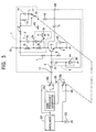
- Fig. 5 is a circuit arrangement diagram showing a third embodiment of the frequency characteristic switchable buffer circuit according to the present invention and shows an example in which a second frequency and a first frequency satisfy a basic wave frequency and its secondary harmonic frequency.
- the frequency characteristic switchable buffer circuit 1 according to the third embodiment is arranged similarly to the buffer circuit 1 according to the first embodiment.
- the front stage of the frequency characteristic switchable buffer circuit 1 according to the third embodiment includes a single voltage-controlled oscillator 24, a second harmonic generator 25, an associating changeover switch 26 composed of two sets of one-circuit two-contacts changeover switches 26 1 and 26 2 , and a power supply 22.
- the front stage of the buffer circuit 1 of the third embodiment is arranged differently from that of the frequency characteristic switchable buffer circuit 1 according to the first embodiment including the first and second voltage-controlled oscillators 20 and 21.
- a changeover switch 11 and the associating changeover switch 26 are switched in association with each other in response to a first or second control signal supplied from a controller (not shown).
- the power supply 22 connected to the second harmonic generator 25 is isolated therefrom by the changeover switch 26 2 , the power supply 22 is connected to only the voltage-controlled oscillator 24, whereby an oscillation signal of the basic wave frequency, for example, an oscillation signal of a second frequency of the 900 MHz is output from the voltage-controlled oscillator 24 and supplied to a signal input terminal 17 of the frequency characteristic switchable buffer circuit 1 through the changeover switches 26 1 .
- the power supply 22 also is connected to the second harmonic generator 25 through the changeover switch 26 2 , whereby the second harmonic generator 25 is put into an operating state.
- the second harmonic generator 25 responds to the basic wave frequency, for example, to the oscillation signal of the second frequency of the 900 MHz band, which is supplied from the voltage-controlled oscillator 24, and outputs its secondary harmonic, for example, an oscillation signal of a first frequency of the 1700 MHz band and the oscillation signal is supplied to the signal input terminal 17 of the frequency characteristic switchable buffer circuit 1 through the changeover switch 26 1 .
- the operation which is performed when the oscillation signal of the second frequency of the 900 MHz band is supplied to the signal input terminal 17 of the frequency characteristic switchable buffer circuit 1 according to the third embodiment is the same as the operation which is performed when the oscillation signal of the second frequency of the 900 MHz band is supplied to the signal input terminal 17 of the frequency characteristic switchable buffer circuit 1 according to the first embodiment.
- the frequency characteristic switchable buffer circuit 1 also not only can greatly increase a amount of attenuation of the signal component of a spurious frequency to the first frequency when the signal of the first frequency (frequency of the 1700 MHz band) is selected but also can greatly increase an amount of attenuation of the signal component of the frequency of the 1700 MHz band which is the spurious frequency of the signal of the second frequency (frequency of the 900 MHz band) when the signal of the second frequency is selected. Therefore, the buffer circuit 1 can selectively output the signal of the first frequency and the signal of the second frequency in which almost no spurious signal component is contained.
- the single oscillator in the present invention is not limited thereto and a single oscillator for generating an oscillation signal of a fixed frequency band may be used.
- the first switching voltage is supplied to the parallel resonant circuit, and the parallel resonant circuit is caused to perform a parallel resonance at the first frequency so as to selectively output a signal of the first frequency.
- the first switching voltage is supplied also to the frequency trap circuit so that the frequency trap circuit is caused to perform a series resonance at a frequency which is lower than the first frequency so as to form a trap to the low frequency as well as when a trap is generated to the side of a frequency which is higher than the first frequency by the rebound of the formation of the above trap, the signal component of the spurious frequency of the signal of the first frequency is attenuated by these traps.
- the second switching voltage is supplied to the parallel resonant circuit, and the parallel resonant circuit is caused to perform a parallel resonance at the second frequency so as to selectively output a signal of the second frequency.
- the second switching voltage is supplied also to the frequency trap circuit so that the frequency trap circuit is caused to perform a series resonance at a frequency in the vicinity of 1700 MHz so as to generate a trap to the frequency in the vicinity of 1700 MHz
- the signal component of the spurious frequency of the second frequency is attenuated by the trap.
- an amount of attenuation of the signal component of the spurious frequency of the signal of the first frequency can be increased.
- an amount of attenuation of the signal component of the spurious frequency of the signal of the second frequency also can be increased. Accordingly, there can be obtained an effect that the first frequency signal and the second frequency signal in which almost no spurious signal component is contained can be selectively output.
Landscapes
- Physics & Mathematics (AREA)
- Nonlinear Science (AREA)
- Inductance-Capacitance Distribution Constants And Capacitance-Resistance Oscillators (AREA)
- Amplifiers (AREA)
- Transceivers (AREA)
- Mobile Radio Communication Systems (AREA)
- Tone Control, Compression And Expansion, Limiting Amplitude (AREA)
Claims (7)
- Circuit tampon à commutation de courbe de réponse en fréquence, comprenant :un étage amplificateur (2, 7, 8) ;un circuit résonant parallèle (3) qui sert de charge de sortie sur ledit étage amplificateur ;un circuit réjecteur de fréquence (6) connecté entre l'entrée dudit étage amplificateur et un potentiel de référence ; etun générateur de tension de commutation de fréquence (11, 12, 13) permettant de générer de manière sélective une première tension de commutation et une deuxième tension de commutation,dans lequel ledit circuit résonant parallèle effectue une résonance parallèle, à une première fréquence, lorsque la première tension de commutation est fournie et effectue une résonance parallèle, à une deuxième fréquence, qui diffère de la première fréquence, lorsque la deuxième tension de commutation est fournie, ledit circuit réjecteur de fréquence est composé d'un circuit série comportant une diode (62) et un condensateur (61), et effectue une résonance série à la deuxième fréquence lorsque la première tension de commutation est fournie, et effectue une résonance série à la première fréquence lorsque la deuxième tension de commutation est fournie.
- Circuit tampon à commutation de courbe de réponse en fréquence selon la revendication 1, dans lequel ledit circuit réjecteur de fréquence est agencé de telle sorte qu'une bobine d'induction (65) est connectée en série au circuit série comportant la diode et le condensateur, et un deuxième condensateur (66) est connecté en parallèle à la diode.
- Circuit tampon à commutation de courbe de réponse en fréquence selon la revendication 1 ou 2, dans lequel la première fréquence est fournie par un premier oscillateur (20) et la deuxième fréquence est fournie par un deuxième oscillateur (21), le premier oscillateur et le deuxième oscillateur sont commutés en alternance dans un état opérationnel et dans un état non opérationnel, lorsque le premier oscillateur se trouve dans l'état opérationnel, ledit générateur de tension de commutation de fréquence est commuté pour générer la première tension de commutation, et lorsque le deuxième oscillateur est dans l'état opérationnel, ledit générateur de tension de commutation de fréquence est commuté pour générer la deuxième tension de commutation.
- Circuit tampon à commutation de courbe de réponse en fréquence selon la revendication 3, dans lequel le premier oscillateur et le deuxième oscillateur sont des oscillateurs commandés en tension.
- Circuit tampon à commutation de courbe de réponse en fréquence selon la revendication 3 ou 4, dans lequel le premier oscillateur sort un signal d'oscillation de la première fréquence d'une bande de 1 700 MHz utilisée dans une communication mobile DSC 1800, et le deuxième oscillateur sort un signal d'oscillation de la deuxième fréquence d'une bande de 900 MHz utilisée dans une communication mobile GSM.
- Circuit tampon à commutation de courbe de réponse en fréquence selon la revendication 1 ou 2, dans lequel la deuxième fréquence et la première fréquence présentent une relation en termes de fréquence d'ondes de base et sa fréquence harmonique, la deuxième fréquence est directement fournie par un oscillateur (24) et la première fréquence est fournie par un oscillateur harmonique (25) auquel est imposée la deuxième fréquence, lorsque la première fréquence est fournie par l'oscillateur, ledit générateur de tension de commutation de fréquence est commuté pour sortir la première tension de commutation, et lorsque la deuxième fréquence est fournie par l'oscillateur harmonique, ledit générateur de tension de commutation de fréquence est commuté pour sortir la deuxième tension de commutation.
- Circuit tampon à commutation de courbe de réponse en fréquence selon la revendication 6, dans lequel l'oscillateur est un oscillateur commandé en tension.
Applications Claiming Priority (4)
| Application Number | Priority Date | Filing Date | Title |
|---|---|---|---|
| JP19800499 | 1999-07-12 | ||
| JP19800499 | 1999-07-12 | ||
| JP2000017368 | 2000-01-26 | ||
| JP2000017368A JP3848512B2 (ja) | 1999-07-12 | 2000-01-26 | 周波数特性が切替可能なバッファ回路 |
Publications (3)
| Publication Number | Publication Date |
|---|---|
| EP1069682A2 EP1069682A2 (fr) | 2001-01-17 |
| EP1069682A3 EP1069682A3 (fr) | 2003-08-13 |
| EP1069682B1 true EP1069682B1 (fr) | 2006-05-31 |
Family
ID=26510718
Family Applications (1)
| Application Number | Title | Priority Date | Filing Date |
|---|---|---|---|
| EP00305781A Expired - Lifetime EP1069682B1 (fr) | 1999-07-12 | 2000-07-07 | Circuit tampon commutable |
Country Status (6)
| Country | Link |
|---|---|
| EP (1) | EP1069682B1 (fr) |
| JP (1) | JP3848512B2 (fr) |
| KR (1) | KR100360360B1 (fr) |
| CN (1) | CN1134192C (fr) |
| DE (1) | DE60028300T2 (fr) |
| TW (1) | TW457763B (fr) |
Families Citing this family (1)
| Publication number | Priority date | Publication date | Assignee | Title |
|---|---|---|---|---|
| CN113111527A (zh) * | 2021-04-20 | 2021-07-13 | 华北电力大学 | 一种单机水电系统切换型频率振荡的近似解析方法 |
Family Cites Families (3)
| Publication number | Priority date | Publication date | Assignee | Title |
|---|---|---|---|---|
| DE1286081B (de) * | 1964-07-08 | 1969-01-02 | Telefunken Patent | Hochfrequenzverstaerker mit einem Transistor |
| JPH09298477A (ja) * | 1995-06-29 | 1997-11-18 | Sony Corp | 短波受信機およびローパスフィルタ |
| JPH10163750A (ja) * | 1996-11-27 | 1998-06-19 | Tdk Corp | 電圧制御発振器 |
-
2000
- 2000-01-26 JP JP2000017368A patent/JP3848512B2/ja not_active Expired - Fee Related
- 2000-06-27 TW TW089112645A patent/TW457763B/zh not_active IP Right Cessation
- 2000-07-07 DE DE60028300T patent/DE60028300T2/de not_active Expired - Fee Related
- 2000-07-07 EP EP00305781A patent/EP1069682B1/fr not_active Expired - Lifetime
- 2000-07-11 CN CNB001207032A patent/CN1134192C/zh not_active Expired - Fee Related
- 2000-07-11 KR KR1020000039539A patent/KR100360360B1/ko not_active Expired - Fee Related
Also Published As
| Publication number | Publication date |
|---|---|
| KR100360360B1 (ko) | 2002-11-13 |
| DE60028300T2 (de) | 2007-05-24 |
| EP1069682A3 (fr) | 2003-08-13 |
| KR20010029921A (ko) | 2001-04-16 |
| EP1069682A2 (fr) | 2001-01-17 |
| CN1134192C (zh) | 2004-01-07 |
| JP3848512B2 (ja) | 2006-11-22 |
| CN1280451A (zh) | 2001-01-17 |
| JP2001085955A (ja) | 2001-03-30 |
| TW457763B (en) | 2001-10-01 |
| DE60028300D1 (de) | 2006-07-06 |
Similar Documents
| Publication | Publication Date | Title |
|---|---|---|
| US6538521B2 (en) | Voltage controlled oscillator | |
| US6366166B1 (en) | Double pass band amplifier circuit and a radio frequency reception head | |
| JP3643259B2 (ja) | バッファ用高周波同調増幅器 | |
| US6288615B1 (en) | Switch-type oscillating circuit for providing isolation between first and second oscillating circuits | |
| EP1092264A4 (fr) | Oscillateur en mode de commutation | |
| EP0961400A2 (fr) | Amplificateur tampon | |
| EP1069682B1 (fr) | Circuit tampon commutable | |
| US6876401B2 (en) | FM-broadcast-receivable television tuner for preventing adjacent-channel interference | |
| US6294961B1 (en) | Selectable voltage-controlled oscillation circuit | |
| US6380813B1 (en) | Frequency-characteristic switchable buffer circuit | |
| KR0137913B1 (ko) | 캐패시터 스위칭 전압제어 발진기 | |
| US20020050866A1 (en) | Voltage controlled oscillator and communication device using the same | |
| US5859573A (en) | Circuit for separating the output of an oscillator from the other parts of a mobile communication system | |
| KR20020084776A (ko) | 다중밴드용 전압제어 발진기 | |
| EP1111771A2 (fr) | Oscillateur commande en tension utilisé en deux gammes de fréquence | |
| JPH104315A (ja) | 高周波発振回路 | |
| US7696833B2 (en) | Oscillator | |
| JP3677396B2 (ja) | 高周波回路 | |
| JP2003198418A (ja) | 高周波スイッチ回路 | |
| JP2005304085A (ja) | 電圧制御発振器 | |
| KR100309227B1 (ko) | 듀얼 밴드 무선단말기의 위상동기루프회로 | |
| JP2006013733A (ja) | 電圧制御発振器 | |
| JPH09252220A (ja) | 電圧制御発振器 | |
| JP2005277882A (ja) | 電圧制御型発振器 | |
| JP2003101345A (ja) | 周波数シフト型電圧制御発振回路 |
Legal Events
| Date | Code | Title | Description |
|---|---|---|---|
| PUAI | Public reference made under article 153(3) epc to a published international application that has entered the european phase |
Free format text: ORIGINAL CODE: 0009012 |
|
| AK | Designated contracting states |
Kind code of ref document: A2 Designated state(s): AT BE CH CY DE DK ES FI FR GB GR IE IT LI LU MC NL PT SE |
|
| AX | Request for extension of the european patent |
Free format text: AL;LT;LV;MK;RO;SI |
|
| PUAL | Search report despatched |
Free format text: ORIGINAL CODE: 0009013 |
|
| AK | Designated contracting states |
Designated state(s): AT BE CH CY DE DK ES FI FR GB GR IE IT LI LU MC NL PT SE |
|
| AX | Request for extension of the european patent |
Extension state: AL LT LV MK RO SI |
|
| RIC1 | Information provided on ipc code assigned before grant |
Ipc: 7H 03F 3/191 B Ipc: 7H 03J 5/24 A |
|
| 17P | Request for examination filed |
Effective date: 20030807 |
|
| AKX | Designation fees paid |
Designated state(s): DE FI FR SE |
|
| GRAP | Despatch of communication of intention to grant a patent |
Free format text: ORIGINAL CODE: EPIDOSNIGR1 |
|
| GRAS | Grant fee paid |
Free format text: ORIGINAL CODE: EPIDOSNIGR3 |
|
| GRAA | (expected) grant |
Free format text: ORIGINAL CODE: 0009210 |
|
| AK | Designated contracting states |
Kind code of ref document: B1 Designated state(s): DE FI FR SE |
|
| PG25 | Lapsed in a contracting state [announced via postgrant information from national office to epo] |
Ref country code: FI Free format text: LAPSE BECAUSE OF FAILURE TO SUBMIT A TRANSLATION OF THE DESCRIPTION OR TO PAY THE FEE WITHIN THE PRESCRIBED TIME-LIMIT Effective date: 20060531 |
|
| REF | Corresponds to: |
Ref document number: 60028300 Country of ref document: DE Date of ref document: 20060706 Kind code of ref document: P |
|
| PG25 | Lapsed in a contracting state [announced via postgrant information from national office to epo] |
Ref country code: SE Free format text: LAPSE BECAUSE OF FAILURE TO SUBMIT A TRANSLATION OF THE DESCRIPTION OR TO PAY THE FEE WITHIN THE PRESCRIBED TIME-LIMIT Effective date: 20060831 |
|
| ET | Fr: translation filed | ||
| PLBE | No opposition filed within time limit |
Free format text: ORIGINAL CODE: 0009261 |
|
| STAA | Information on the status of an ep patent application or granted ep patent |
Free format text: STATUS: NO OPPOSITION FILED WITHIN TIME LIMIT |
|
| 26N | No opposition filed |
Effective date: 20070301 |
|
| PGFP | Annual fee paid to national office [announced via postgrant information from national office to epo] |
Ref country code: DE Payment date: 20070924 Year of fee payment: 8 |
|
| PGFP | Annual fee paid to national office [announced via postgrant information from national office to epo] |
Ref country code: FR Payment date: 20070622 Year of fee payment: 8 |
|
| PG25 | Lapsed in a contracting state [announced via postgrant information from national office to epo] |
Ref country code: DE Free format text: LAPSE BECAUSE OF NON-PAYMENT OF DUE FEES Effective date: 20090203 |
|
| REG | Reference to a national code |
Ref country code: FR Ref legal event code: ST Effective date: 20090331 |
|
| PG25 | Lapsed in a contracting state [announced via postgrant information from national office to epo] |
Ref country code: FR Free format text: LAPSE BECAUSE OF NON-PAYMENT OF DUE FEES Effective date: 20080731 |