EP1069603A1 - Fertigungseinrichtung - Google Patents
Fertigungseinrichtung Download PDFInfo
- Publication number
- EP1069603A1 EP1069603A1 EP99937830A EP99937830A EP1069603A1 EP 1069603 A1 EP1069603 A1 EP 1069603A1 EP 99937830 A EP99937830 A EP 99937830A EP 99937830 A EP99937830 A EP 99937830A EP 1069603 A1 EP1069603 A1 EP 1069603A1
- Authority
- EP
- European Patent Office
- Prior art keywords
- slit
- baffle plate
- tapered surface
- process chamber
- exhaust passage
- Prior art date
- Legal status (The legal status is an assumption and is not a legal conclusion. Google has not performed a legal analysis and makes no representation as to the accuracy of the status listed.)
- Withdrawn
Links
Images


Classifications
-
- H—ELECTRICITY
- H01—ELECTRIC ELEMENTS
- H01J—ELECTRIC DISCHARGE TUBES OR DISCHARGE LAMPS
- H01J37/00—Discharge tubes with provision for introducing objects or material to be exposed to the discharge, e.g. for the purpose of examination or processing thereof
- H01J37/32—Gas-filled discharge tubes
- H01J37/32431—Constructional details of the reactor
- H01J37/32798—Further details of plasma apparatus not provided for in groups H01J37/3244 - H01J37/32788; special provisions for cleaning or maintenance of the apparatus
- H01J37/32816—Pressure
- H01J37/32834—Exhausting
- H01J37/32844—Treating effluent gases
-
- H—ELECTRICITY
- H01—ELECTRIC ELEMENTS
- H01J—ELECTRIC DISCHARGE TUBES OR DISCHARGE LAMPS
- H01J37/00—Discharge tubes with provision for introducing objects or material to be exposed to the discharge, e.g. for the purpose of examination or processing thereof
- H01J37/32—Gas-filled discharge tubes
- H01J37/32431—Constructional details of the reactor
- H01J37/32798—Further details of plasma apparatus not provided for in groups H01J37/3244 - H01J37/32788; special provisions for cleaning or maintenance of the apparatus
- H01J37/32816—Pressure
- H01J37/32834—Exhausting
-
- H—ELECTRICITY
- H01—ELECTRIC ELEMENTS
- H01J—ELECTRIC DISCHARGE TUBES OR DISCHARGE LAMPS
- H01J37/00—Discharge tubes with provision for introducing objects or material to be exposed to the discharge, e.g. for the purpose of examination or processing thereof
- H01J37/32—Gas-filled discharge tubes
- H01J37/32431—Constructional details of the reactor
- H01J37/32623—Mechanical discharge control means
- H01J37/32633—Baffles
-
- Y—GENERAL TAGGING OF NEW TECHNOLOGICAL DEVELOPMENTS; GENERAL TAGGING OF CROSS-SECTIONAL TECHNOLOGIES SPANNING OVER SEVERAL SECTIONS OF THE IPC; TECHNICAL SUBJECTS COVERED BY FORMER USPC CROSS-REFERENCE ART COLLECTIONS [XRACs] AND DIGESTS
- Y02—TECHNOLOGIES OR APPLICATIONS FOR MITIGATION OR ADAPTATION AGAINST CLIMATE CHANGE
- Y02C—CAPTURE, STORAGE, SEQUESTRATION OR DISPOSAL OF GREENHOUSE GASES [GHG]
- Y02C20/00—Capture or disposal of greenhouse gases
- Y02C20/30—Capture or disposal of greenhouse gases of perfluorocarbons [PFC], hydrofluorocarbons [HFC] or sulfur hexafluoride [SF6]
-
- Y—GENERAL TAGGING OF NEW TECHNOLOGICAL DEVELOPMENTS; GENERAL TAGGING OF CROSS-SECTIONAL TECHNOLOGIES SPANNING OVER SEVERAL SECTIONS OF THE IPC; TECHNICAL SUBJECTS COVERED BY FORMER USPC CROSS-REFERENCE ART COLLECTIONS [XRACs] AND DIGESTS
- Y02—TECHNOLOGIES OR APPLICATIONS FOR MITIGATION OR ADAPTATION AGAINST CLIMATE CHANGE
- Y02P—CLIMATE CHANGE MITIGATION TECHNOLOGIES IN THE PRODUCTION OR PROCESSING OF GOODS
- Y02P70/00—Climate change mitigation technologies in the production process for final industrial or consumer products
- Y02P70/50—Manufacturing or production processes characterised by the final manufactured product
Definitions
- the present invention relates to a process apparatus for performing a process, such as etching, on an object such as a semiconductor wafer.
- a magnetron-type plasma process apparatus that is generally known comprises a gas-tight process vessel, an upper electrode provided in the vessel, a lower electrode provided in the vessel and opposing the upper electrode, and a magnet surrounding a plasma region provided between the upper and lower electrodes.
- the object is mounted on the lower electrode. Then, the process gas is introduced into the process vessel.
- the process vessel is evacuated, whereby a low-pressure atmosphere is maintained in the vessel. Thereafter, high-frequency power is supplied to the lower electrode, thereby generating plasma in the process vessel.
- a plasma process apparatus of this type has a baffle plate, which partitions the process vessel into a process chamber and an exhaust passage.
- An object to be processed is placed in the process chamber.
- the exhaust passage communicates with an evacuation mechanism.
- the baffle plate is provided between the side of the lower electrode and the inner surface of the process vessel and surrounds the lower electrode.
- the baffle plate has a plurality of slits that extend in the radial direction, connecting the process chamber and the exhaust passage. (The chamber and the passage communicate with each other through these slits.)
- the baffle plate partitions the plasma region while the process is undergoing. This increases the density of plasma in the process chamber.
- the conductance between the process chamber and the exhaust passage is maintained in a prescribed condition since the gas is guided from the chamber into the passage through the slits.
- the gas can be exhausted from the process chamber in a stable condition.
- the baffle plate has the function of holding the reaction product made by the process, thus reducing the amount in which the reduction product flows into the exhaust passage.
- the reaction product deposits on that surface of the baffle plate which is exposed to the process chamber (i.e., the surface of the plate facing the chamber).
- the amount of deposition is proportional to the time of process. If the product deposits on the rims of the slits though which the gas flows from the process chamber, the slits will become narrower. Consequently, the pressure in the process chamber will rise. This impairs the uniformity of etching in the plane of the object (i.e., in-plane uniformity) or decrease the etching rate.
- the maintenance of the baffle plate is effected at regular intervals, by either washing the plate or replacing it with a new one. If the process generates deposit in large quantities, however, the maintenance must be carried out more frequently. In this case, the throughput of the process will decrease.
- the object of the invention is to provide a novel, improved process apparatus in which the slits of the baffle plate are hardly narrowed with deposit on the chamber side, an atmosphere of a prescribed pressure can therefore be maintained in the process chamber for a long time (that is, the process time can be lengthened without changing the process conditions), and the maintenance cycle of the baffle plate can be thereby extended to enhance the throughput of the process.
- a process apparatus includes an airtight process vessel, an exhaust system for exhausting gas from the process vessel, and a baffle plate for partitioning the process vessel into a process chamber for processing an object and an exhaust passage communicating with the exhaust system.
- the baffle plate has a plurality of slits through which the process chamber and the exhaust passage communicate with each other, and each of the slits has a tapered surface on an inner surface toward the process chamber, the tapered surface being formed to not less than 1/4 of a depth of the slit.
- angle ⁇ between the tapered surface and a perpendicular crossing an open end of the slit at right angles fall within a range from 5° to 30° (5° ⁇ ⁇ ⁇ 30° ).
- each slit has an enlarged opening facing the exhaust passage, extending from an opening rim of the slit, which faces the exhaust passage, toward the process chamber, and having an inside diameter which is larger than the minimum inside diameter of a process-chamber-side portion of the slit on which the tapered surface is formed, it is preferable that the tapered surface and the enlarged opening be each formed to 1/4 to 1/2 of the depth of the slit and angle ⁇ between the tapered surface and a perpendicular crossing an open end of the slit at right angles fall within a range from 30° to 60° (30° ⁇ ⁇ ⁇ 60° ).
- width W1 of an opening of the slit, which faces the process chamber, and width W2 of an opening of the slit, which faces the exhaust passage, are set so as to satisfy a condition of 1 ⁇ W2/W1 ⁇ 1.4.
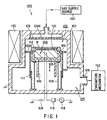
- FIG. 1 shows a magnetron-type plasma etching apparatus that is a process apparatus according to the present invention.
- the etching apparatus 100 has a process vessel 102 made of aluminum and connected to the ground.
- An oxide aluminum film has been formed on the process vessel 102 by means of, for example, anodic oxidation.
- a lower electrode 104 is arranged in the process vessel 102.
- the lower electrode 104 serves as a susceptor that has a mounting surface on which an object to be processed, e.g., a semiconductor wafer W (hereinafter referred to as "wafer”), may be mounted.
- a semiconductor wafer W hereinafter referred to as "wafer
- the lower electrode 104 is covered, except for the mounting surface, with an insulating member 105 made of, for example, ceramics, and a conductive member 107 made of, for example, aluminum.
- the lower electrode 104 can be moved up and down as lifting shafts 106 are driven.
- Bellows 109 made of, for example, stainless steel are provided between the conductive member 107 and the process vessel 102.
- the conductive member 107 and process vessel 102 contact the bellows 109, with no aluminum film interposed between them and the bellows 109 (or with an aluminum film removed). Therefore, the conductive member 107 is connected to the ground by the bellows 109 and the process vessel 102.
- a bellows cover 111 is provided, surrounding the conductive member 107 and bellows 109.
- an electrostatic chuck 110 connected to a high-voltage DC power supply 108 is provided on the mounting surface of the lower electrode 104.
- An insulating focus ring 112 is arranged, surrounding the electrostatic chuck 110.
- a high-frequency power supply 118 for outputting high-frequency power is connected to a matching device 116, which in turn is connected to the lower electrode 104.
- An upper electrode 126 is provided on the inner surface of the process vessel 102, which opposes the mounting surface of the lower electrode 104.
- the upper electrode 126 has a number of gas outlet holes 126a.
- the gas outlet holes 126a communicate with a gas-supplying source 150 that supplies process gas.
- the process gas supplied from the gas-supplying source 150 is therefore introduced into a process chamber 122 through the gas outlet holes 126a.
- An exhaust pipe 128 is connected, at one end, to a lower port of the process vessel 102 and, at the other end, to an evacuation mechanism 152.
- a magnet 130 is arranged outside the process vessel 102, for confining plasma generated between the lower electrode 104 and the upper electrode 126.
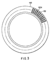
- a baffle plate 120 is arranged beside the lower electrode 104, partitioning the interior of the process vessel into the process chamber 122 for processing the wafer and the exhaust passage 124 communicating with the exhaust pipe 128.
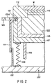
- the baffle plate 120 is located between the circumferential surface of the lower electrode 104 and the inner surface of the process vessel 102 and surrounds the lower electrode 104. More specifically, the baffle plate 120 is clamped between the focus ring 112 and the conductive member 107. As shown in FIG. 2, the plate 120 is secured to the top of the conductive member 107 by electrically conductive screws 121.
- the baffle plate 120 is made of electrically conductive material such as aluminum and has a surface oxidized by anodic oxidation.
- the baffle plate 120 and the conductive member 107 contact each other, with no aluminum oxide film interposed between them. In other words, the aluminum oxide film has been removed from that part of the plate 120 which contacts the conductive member 107.
- the baffle plate 120 is therefore connected to the ground by the conductive member 107, bellows 109 and process vessel 102 and remains at almost the same potential (ground potential) as the inner wall of the process vessel 102.
- the baffle plate 120 and the inner wall of the vessel 102 which is located above the baffle plate 120, function as counter electrodes of the lower electrode 104. Plasma can, therefore, be confined in a space above the baffle plate 120, that is, within the process chamber 122.
- the baffle plate 120 is shaped almost like a ring.
- the plate 120 has a thickness that falls within the range from 1 mm to 20 mm. In the present embodiment, the plate 120 is 3 mm thick.
- the baffle plate 120 has a plurality of slits, e.g., 360 slits 120a arranged on the entire circumferential surface of the plate 120 in order to cause the process chamber 122 and exhaust passage 124 to communicate with each other when the baffle plate 120 is mounted on the lower electrode 104. More precisely, the slits 120a extend in radial directions of the baffle plate 120. The number of slits 120a can be changed to any value, ranging from 180 to 540, in accordance with the process apparatus to which the baffle plate 120 is applied.
- the slits 120a (arranged in the radial directions of the baffle plate 120) have a length that falls within the range from 35 mm to 45 mm. In the present embodiment, the length is set to 41 mm.
- the slits 120a have a width that falls within the range from 0.5 mm to 2.5 mm. In the present embodiment, the width is set to 1.6 mm.
- the area of the opening of each slit 120a, which faces the process chamber 122, is 25% to 75% of that of the surface (top) of the baffle plate 120 which faces the chamber 122. In the present embodiment, it is set to 54%.
- FIG. 1 illustrates, when the baffle plate 120 is arranged between the side of the lower electrode 104 and the inner surface of the process vessel 102, only the minimum gap, which does not prevent the lower electrode 104 from moving up and down, is formed between the outer surface of the baffle plate 120 and the inner surface of the process vessel 102.
- the gas in the process chamber 122 is therefore exhausted from the exhaust passage 124 into an exhaust pipe 128 only through the slits 120a of the baffle plate 120.
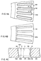
- each of the slits 120a has a tapered surface 132 toward the process chamber 122.
- the tapered surface 132 extends in the radial direction of the baffle plate 120 on either side of the slit 120a and inclines from the rim of the slit 120a, which faces the process chamber 122, toward the exhaust passage 124 in which direction the opening of the slit 120a is narrowed.
- the taper depth h is set to three fourths of the slit depth H.
- the angle (hereinafter referred to as "taper angle") ⁇ between the tapered surface 132 and a perpendicular 136 (a line crossing the open ends 132a and 134 at right angles) falls within the range from 5° to 30° (5° ⁇ ⁇ ⁇ 30° ). In the present embodiment, the angle ⁇ is set to 10° .
- FIG. 6 shows an example of deposit a deposited on a conventional baffle plate X.
- each slit S has a tapered surface T toward the process chamber, and the tapered surface T is formed by chamfering in order to prevent the rim of the slit S from being damaged due to a plasma atmosphere.
- the taper depth h of the taper surface T is about one sixth of the slit depth H, while the taper angle ⁇ of the tapered surface T is 45° . Therefore, the deposit a greatly juts into the slit S and the inside diameter R1 of the slit S is shortened in a short time (FIG.
- FIG. 6 shows the condition in which the inside diameter R1 of the slit S is decreased to R2 by the deposit a ).
- the flow rate of gas passing through the slit S lowers in a relatively short time, and the pressure in the process chamber rises in a relatively short time.
- the uniformity of etching in the plane of a wafer W in-plane uniformity
- the etching rate decreases in a short time, too. Consequently, the maintenance of the baffle plate X must be carried out more frequently, and the throughput of the process will decrease.
- FIG. 5 shows an example of a deposit a deposited on the baffle plate 120 of the present embodiment. If, as shown, the taper depth h is not less than half the slit depth H and the taper angle ⁇ ranges from 5° to 30° (5° ⁇ ⁇ ⁇ 30° ), the deposit a is deposited gradually from the top of the tapered surface 132. The opening of the slit 120a, which faces the process chamber 122, is hardly narrowed by the deposit a , and it takes a considerably long time to make the inside diameter of the slit 120a smaller than the prescribed value R1.
- the gas in the process chamber 122 is allowed to pass through the slit 120a without resistance for a long time, and a given pressure is maintained in the process chamber 122 for a long time (the process time can be lengthened more than the conventional one without changing any process conditions). Consequently, the uniformity of etching in the plane of the wafer W (in-plane uniformity) is maintained for a long time, as is the high etching rate.
- the maintenance cycle of the baffle plate 120 can be extended to enhance the throughput of the process (by securing a long time for which the baffle plate 120 can be processed continuously without maintenance or exchange). The following are experimental data to support the advantages of the baffle plate 120 of the present invention.
- the experiment was performed under the same process (etching) conditions when two baffle plates to be compared were attached separately to the same plasma etching apparatus 100 (see FIG. 1).
- the conventional baffle plate X is the same as the baffle plate 120 except for taper depth h and taper angle ⁇ .
- FIG. 7 shows variations in pressure in process chamber 122 with process time.
- the time required until the pressure atmosphere reaches 65 mTorr therefore corresponds to continuous process time.
- the pressure atmosphere in the process chamber 122 arrived at 65 mTorr in about 85 hours.
- the pressure atmosphere arrived at 65 mTorr in about 40 hours.
- the continuous process time can be extended more greatly than using the conventional baffle plate X. If, in particular, the baffle plate 120 is used, the continuous process time can be extended two or more times as long as that in the case of the conventional baffle plate.
- FIG. 8 shows variations in etching rate with process time.
- the etching process could be performed at a high etching rate of about 270 nm per minute if the process time did not exceed about 100 hours.
- the etching process could be performed at the same etching rate as that of the present invention if the process time did not exceed about 40 hours; however, the etching rate lowered abruptly immediately after the process time exceeded 40 hours.
- baffle plate 120 If the baffle plate 120 is used, a desired uniform etching rate can be achieved even after a lapse of process time which is two or more times as long as that in the case of the conventional baffle plate X.
- the in-plane uniformity of ⁇ 5% could be obtained if the process time did not exceed about 80 hours.
- the conventional baffle plate X was used, the same in-plane uniformity as that of the present invention could be obtained if the process time did not exceed about 20 hours; however, the value of the in-plane uniformity increased when the process time exceeded 20 hours and it increased abruptly immediately after the process time exceeded 40 hours.
- baffle plate 120 If the baffle plate 120 is used, prescribed in-plane-uniformity can be achieved even after a lapse of process time which is four or more times as long as that in the case of the conventional baffle plate X.
- the taper depth h of the tapered surface 132 is set not less than half the slit depth H and the taper angle ⁇ falls within the range from 5° to 30° (5° ⁇ ⁇ ⁇ 30° ). Since the depth of the taper surface 132 is considerably greater (1/2 or more of the slit depth H in substance), the area of the tapered surface can be enlarged more greatly than that of the conventional baffle plate X, keeping the conductance of the process chamber 122 and exhaust passage 124 in prescribed conditions. Since, moreover, the taper angle ⁇ falls within the range from 5° to 30° (5° ⁇ ⁇ 30° ), a deposit is formed effectively on the tapered surface 132.
- a deposit such as a reaction product is formed on the baffle plate 120 in sequence from the top of the tapered surface 132, and the openings of the slits 120a, which face the process chamber 122, are hardly narrowed by the deposit.
- gas in the process chamber 122 can be caused to pass through the slits 120a for a long time without resistance and a given process pressure is maintained in the process chamber 122 for a long time (it is possible to extend time required until a pressure atmosphere of the process chamber 122 increases due to clogging of the slits 120a).
- the process time can be extended longer than that in the prior art without changing process conditions.
- the in-plane uniformity and etching rate of the wafer W can be maintained high for a long time, and the maintenance cycle of the baffle plate 120 can be extended more greatly than that in the prior art to improve the throughput of the process.
- each slit 120a is not increased but the slit 120a has a large tapered surface 132 with a given depth and angle which opposes the process chamber 122.
- the process time can be extended without exercising an influence on the conductance in the process chamber 122 and exhaust passage 124.
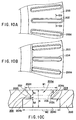
- FIGS. 10A to 10C illustrate a modification to the baffle plate of the embodiment described above.
- a plurality of slits 200a are arranged on the entire circumferential surface of the plate 200 in order to cause the process chamber 122 and exhaust passage 124 to communicate with each other when the baffle plate 200 is mounted on the lower electrode 104. More specifically, the slits 200a extend in radial directions of the baffle plate 200. As shown in FIGS. 10A and 10C, each of the slits 200a has a tapered surface 202 toward the process chamber 122. As illustrated in FIGS. 10B and 10C, an enlarged opening 204 is provided toward the exhaust passage 124 of the slits 200a.
- the tapered surface 202 extends in the radial direction of the baffle plate 200 on either side of the slit 200a and inclines from the rim of the slit 200a, which faces the process chamber 122, toward the exhaust passage 124 in which direction the opening of the slit 200a is narrowed.
- the distance between an open end 202a of the slit 200a, which opposes the process chamber 122, and a region 202b surrounded by the lower rim 202c of the tapered surface 202, i.e., the taper depth h1 is substantially 1/4 to 1/2 of the distance between the open end 202a and the other open end 204a of the slit 200a (enlarged opening 204), which opposes the exhaust passage 124, i.e., the slit depth H.
- the taper depth h1 is set to one third of the slit depth H.
- the angle between the tapered surface 202 and a perpendicular 206 i.e., the taper angle ⁇ falls within the range from 30° to 60° (30° ⁇ ⁇ ⁇ 60° ) in substance. In the present modification, the angle ⁇ is set to 45° .
- the enlarged opening 204 is shaped almost like a trench and formed along the radial direction of the baffle plate 200 alongside the exhaust passage 124 of the slit 200a.
- the distance h2 between the open end 204a of the opening 204, which opposes the exhaust passage 124, and a region 204b surrounded by a bottom rim 204c of the opening 204 (hereinafter referred to as "enlarged opening depth") is 1/4 to 1/2 of the slit depth H in substance.
- the distance h2 is set to 1/2 of the slit depth H.
- the area of the open end 204a of the enlarged opening 204 is set larger than that of the region 202b of the lower rim 202c of the tapered surface 202.
- the width W1 of the slit 200a, which faces the process chamber 122, and the width W2 of the slit 200a, which faces the exhaust passage 124, are set so as to satisfy the condition of 1 ⁇ W2/W1 ⁇ 1.4 in substance.
- W2/W1 is set at 1.2.
- the baffle plate 200 having the above-described structure was applied to the etching apparatus 100 shown in FIG. 1 and the wafer W (which is identical with that used in the above experiments) was processed by etching under the same process conditions as those of the above experiments. It was 60 hours or longer before the pressure atmosphere in the process chamber 122 reached 65 mTorr. Even when the same experiments were carried out by changing only the taper angle ⁇ of the tapered surface to 30° , 40° , 50° and 60° , it was 60 hours or longer before the pressure atmosphere in the process chamber 122 reached 65 mTorr in each case.
- the continuous process time can be extended more greatly than using the conventional baffle plate X. Further, even when the same experiments were performed by changing only the value of W2/W1 to 1 and 1.4, it was 60 hours or longer before the pressure atmosphere in the process chamber 122 reached 65 mTorr in either case. If, therefore, W2/W1 is properly set within the range from 1 to 1.4 in substance in the baffle plate 200 having the enlarged opening 204, the continuous process time can be extended more greatly than using the conventional baffle plate X.
- the taper depth h1 of the tapered surface 202 is 1/4 to 1/2 of the slit depth H and the taper angle ⁇ falls within the range from 30° to 60° (30° ⁇ ⁇ ⁇ 60° ).
- the depth of the tapered surface 202 is therefore considerably greater, the area of the tapered surface can be enlarged more greatly than that of the conventional baffle plate X, keeping the conductance of the process chamber 122 and exhaust passage 124 in prescribed conditions. Since, moreover, the taper angle ⁇ falls within the range from 30° to 60° (30° ⁇ ⁇ ⁇ 60° ), a deposit is formed effectively on the tapered surface 202.
- a deposit such as a reaction product is formed on the baffle plate 200 in sequence from the top of the tapered surface 202, and the openings of the slits 200a, which face the process chamber 122, are hardly narrowed by the deposit.
- gas in the process chamber 122 can be caused to pass through the slits 200a for a long time without resistance and a given process pressure is maintained in the process chamber 122 for a long time.
- the process time can be extended longer than that in the prior art without changing process conditions. Consequently, the in-plane uniformity and etching rate of the wafer W can be maintained high for a long time, and the maintenance cycle of the baffle plate 200 can be extended more greatly than that in the prior art to improve the throughput of the process.
- the baffle plate 200 of the present modification has the enlarged opening 204 having a large opening area toward the exhaust passage 124 of the slit 200a and the depth h2 of the enlarged opening is set to 1/4 to 1/2 of the slit depth H in substance. Consequently, a small-diameter portion in the slit 200a on which a deposit is easily formed, can be decreased, and time can be extended further until the process chamber 122 increases in pressure. Since, in the present modification, the area of the open end 204a of the enlarged opening 204 is set larger than that of the region 202b surrounded by the lower rim 202c of the tapered surface 202, gas can be uniformly guided to the exhaust passage 124 through the slits 200 without any disturbance.
- the width W1 of the slit 200a, which faces the process chamber 122, and the width W2 of the slit 200a, which faces the exhaust passage 124, are set so as to satisfy the condition of 1 ⁇ W2/W1 ⁇ 1.4 in substance. Therefore, time can be extended further until the opening of the slit 200a is narrowed by the deposit, without exercising an influence on the conductance in the process chamber 122 and exhaust passage 124.
- the conductance in the process chamber 122 and exhaust passage 124 can thus be maintained in a desired condition even though the slit 200a is provided with the tapered surface 202 and enlarged opening 204.
- the width of the slit 120a is constant on both the inner and outer sides of the baffle plate 120; however, it can be varied as shown in FIG. 11.
- width W4 on the outer side is set greater than width W3 on the inner side.
- corner portions are formed at the upper rim (opening rim) of the tapered surface 132 (202), the lower rim 132c (202c) of the tapered surface 132 (202), the bottom of the enlarged opening 204, and the open end 204a of the opening 204; however, these corner portions can be chamfered.
- the wafer is processed by etching by C 4 F 8 , CO and Ar.
- the present invention can be applied to another process apparatus such as a plasma CVD apparatus and a process of another object such as an LCD glass substrate.
Landscapes
- Physics & Mathematics (AREA)
- Engineering & Computer Science (AREA)
- Plasma & Fusion (AREA)
- Chemical & Material Sciences (AREA)
- Analytical Chemistry (AREA)
- Drying Of Semiconductors (AREA)
Applications Claiming Priority (5)
| Application Number | Priority Date | Filing Date | Title |
|---|---|---|---|
| JP7343398 | 1998-03-06 | ||
| JP7343398 | 1998-03-06 | ||
| JP17961698 | 1998-06-11 | ||
| JP17961698A JP4217299B2 (ja) | 1998-03-06 | 1998-06-11 | 処理装置 |
| PCT/JP1999/001055 WO1999045584A1 (en) | 1998-03-06 | 1999-03-04 | Processing apparatus |
Publications (2)
| Publication Number | Publication Date |
|---|---|
| EP1069603A1 true EP1069603A1 (de) | 2001-01-17 |
| EP1069603A4 EP1069603A4 (de) | 2007-01-10 |
Family
ID=26414574
Family Applications (1)
| Application Number | Title | Priority Date | Filing Date |
|---|---|---|---|
| EP99937830A Withdrawn EP1069603A4 (de) | 1998-03-06 | 1999-03-04 | Fertigungseinrichtung |
Country Status (5)
| Country | Link |
|---|---|
| US (1) | US6733620B1 (de) |
| EP (1) | EP1069603A4 (de) |
| JP (1) | JP4217299B2 (de) |
| KR (1) | KR100536313B1 (de) |
| WO (1) | WO1999045584A1 (de) |
Cited By (11)
| Publication number | Priority date | Publication date | Assignee | Title |
|---|---|---|---|---|
| WO2004030015A3 (en) * | 2002-09-30 | 2004-06-03 | Tokyo Electron Ltd | Method and apparatus for an improved baffle plate in a plasma processing system |
| WO2005048322A3 (en) * | 2003-11-12 | 2005-11-24 | Tokyo Electron Ltd | Method and apparatus for improved baffle plate |
| US7137353B2 (en) | 2002-09-30 | 2006-11-21 | Tokyo Electron Limited | Method and apparatus for an improved deposition shield in a plasma processing system |
| US7147749B2 (en) | 2002-09-30 | 2006-12-12 | Tokyo Electron Limited | Method and apparatus for an improved upper electrode plate with deposition shield in a plasma processing system |
| US7163585B2 (en) | 2002-09-30 | 2007-01-16 | Tokyo Electron Limited | Method and apparatus for an improved optical window deposition shield in a plasma processing system |
| US7166200B2 (en) | 2002-09-30 | 2007-01-23 | Tokyo Electron Limited | Method and apparatus for an improved upper electrode plate in a plasma processing system |
| US7204912B2 (en) | 2002-09-30 | 2007-04-17 | Tokyo Electron Limited | Method and apparatus for an improved bellows shield in a plasma processing system |
| US7282112B2 (en) | 2002-09-30 | 2007-10-16 | Tokyo Electron Limited | Method and apparatus for an improved baffle plate in a plasma processing system |
| US7291566B2 (en) | 2003-03-31 | 2007-11-06 | Tokyo Electron Limited | Barrier layer for a processing element and a method of forming the same |
| WO2008021654A3 (en) * | 2006-08-11 | 2008-07-31 | Tokyo Electron Ltd | Exhaust assembly for a plasma processing system and method |
| US7585384B2 (en) | 2003-04-17 | 2009-09-08 | Applied Materials, Inc. | Apparatus and method to confine plasma and reduce flow resistance in a plasma reactor |
Families Citing this family (64)
| Publication number | Priority date | Publication date | Assignee | Title |
|---|---|---|---|---|
| TW514996B (en) * | 1999-12-10 | 2002-12-21 | Tokyo Electron Ltd | Processing apparatus with a chamber having therein a high-corrosion-resistant sprayed film |
| JP4592856B2 (ja) * | 1999-12-24 | 2010-12-08 | 東京エレクトロン株式会社 | バッフル板及びガス処理装置 |
| JP4602532B2 (ja) * | 2000-11-10 | 2010-12-22 | 東京エレクトロン株式会社 | プラズマ処理装置 |
| KR100689810B1 (ko) * | 2001-04-11 | 2007-03-08 | 삼성전자주식회사 | 반도체장치 제조용 식각장치의 배플 |
| US20030092278A1 (en) * | 2001-11-13 | 2003-05-15 | Fink Steven T. | Plasma baffle assembly |
| US20040129218A1 (en) * | 2001-12-07 | 2004-07-08 | Toshiki Takahashi | Exhaust ring mechanism and plasma processing apparatus using the same |
| JP4061062B2 (ja) * | 2001-12-13 | 2008-03-12 | ローム株式会社 | 半導体発光素子の製法および酸化炉 |
| JP2003224077A (ja) * | 2002-01-30 | 2003-08-08 | Tokyo Electron Ltd | プラズマ処理装置、電極部材、バッフル板の製造方法、処理装置、および、表面処理方法 |
| KR20030090305A (ko) * | 2002-05-22 | 2003-11-28 | 동경엘렉트론코리아(주) | 플라즈마 발생장치의 가스 배기용 배플 플레이트 |
| US7494560B2 (en) * | 2002-11-27 | 2009-02-24 | International Business Machines Corporation | Non-plasma reaction apparatus and method |
| US7780786B2 (en) | 2002-11-28 | 2010-08-24 | Tokyo Electron Limited | Internal member of a plasma processing vessel |
| US7560376B2 (en) | 2003-03-31 | 2009-07-14 | Tokyo Electron Limited | Method for adjoining adjacent coatings on a processing element |
| KR100563818B1 (ko) * | 2003-08-01 | 2006-03-28 | 동부아남반도체 주식회사 | 플라즈마 에칭 챔버의 배플 플레이트를 위한 치구 |
| JP2005260011A (ja) * | 2004-03-12 | 2005-09-22 | Hitachi High-Technologies Corp | ウエハ処理装置およびウエハ処理方法 |
| US7552521B2 (en) | 2004-12-08 | 2009-06-30 | Tokyo Electron Limited | Method and apparatus for improved baffle plate |
| US7601242B2 (en) | 2005-01-11 | 2009-10-13 | Tokyo Electron Limited | Plasma processing system and baffle assembly for use in plasma processing system |
| US20070028838A1 (en) * | 2005-07-29 | 2007-02-08 | Craig Bercaw | Gas manifold valve cluster |
| US7718030B2 (en) * | 2005-09-23 | 2010-05-18 | Tokyo Electron Limited | Method and system for controlling radical distribution |
| CN100416757C (zh) * | 2005-12-07 | 2008-09-03 | 北京北方微电子基地设备工艺研究中心有限责任公司 | 等离子体刻蚀装置排气环 |
| US8141514B2 (en) * | 2006-03-23 | 2012-03-27 | Tokyo Electron Limited | Plasma processing apparatus, plasma processing method, and storage medium |
| US8104428B2 (en) * | 2006-03-23 | 2012-01-31 | Tokyo Electron Limited | Plasma processing apparatus |
| US20080100427A1 (en) * | 2006-10-25 | 2008-05-01 | Siemens Vdo Automotive Corporation | Configurable protocol identification device |
| JP2009200184A (ja) * | 2008-02-20 | 2009-09-03 | Tokyo Electron Ltd | プラズマ処理装置及びプラズマ処理装置のバッフル板 |
| US8075728B2 (en) * | 2008-02-28 | 2011-12-13 | Applied Materials, Inc. | Gas flow equalizer plate suitable for use in a substrate process chamber |
| US7987814B2 (en) * | 2008-04-07 | 2011-08-02 | Applied Materials, Inc. | Lower liner with integrated flow equalizer and improved conductance |
| JP5102706B2 (ja) * | 2008-06-23 | 2012-12-19 | 東京エレクトロン株式会社 | バッフル板及び基板処理装置 |
| US8597462B2 (en) | 2010-05-21 | 2013-12-03 | Lam Research Corporation | Movable chamber liner plasma confinement screen combination for plasma processing apparatuses |
| CN103377979B (zh) * | 2012-04-30 | 2016-06-08 | 细美事有限公司 | 调节板和具有该调节板的用于处理基板的装置 |
| CN103578906B (zh) * | 2012-07-31 | 2016-04-27 | 细美事有限公司 | 用于处理基板的装置 |
| US9132436B2 (en) | 2012-09-21 | 2015-09-15 | Applied Materials, Inc. | Chemical control features in wafer process equipment |
| US10256079B2 (en) | 2013-02-08 | 2019-04-09 | Applied Materials, Inc. | Semiconductor processing systems having multiple plasma configurations |
| JP6438320B2 (ja) * | 2014-06-19 | 2018-12-12 | 東京エレクトロン株式会社 | プラズマ処理装置 |
| US11637002B2 (en) | 2014-11-26 | 2023-04-25 | Applied Materials, Inc. | Methods and systems to enhance process uniformity |
| JP6423706B2 (ja) * | 2014-12-16 | 2018-11-14 | 東京エレクトロン株式会社 | プラズマ処理装置 |
| US20160225652A1 (en) | 2015-02-03 | 2016-08-04 | Applied Materials, Inc. | Low temperature chuck for plasma processing systems |
| US9741593B2 (en) | 2015-08-06 | 2017-08-22 | Applied Materials, Inc. | Thermal management systems and methods for wafer processing systems |
| US10504700B2 (en) | 2015-08-27 | 2019-12-10 | Applied Materials, Inc. | Plasma etching systems and methods with secondary plasma injection |
| US10504754B2 (en) | 2016-05-19 | 2019-12-10 | Applied Materials, Inc. | Systems and methods for improved semiconductor etching and component protection |
| US9865484B1 (en) | 2016-06-29 | 2018-01-09 | Applied Materials, Inc. | Selective etch using material modification and RF pulsing |
| US10546729B2 (en) | 2016-10-04 | 2020-01-28 | Applied Materials, Inc. | Dual-channel showerhead with improved profile |
| US11276559B2 (en) | 2017-05-17 | 2022-03-15 | Applied Materials, Inc. | Semiconductor processing chamber for multiple precursor flow |
| US11276590B2 (en) | 2017-05-17 | 2022-03-15 | Applied Materials, Inc. | Multi-zone semiconductor substrate supports |
| JP7176860B6 (ja) | 2017-05-17 | 2022-12-16 | アプライド マテリアルズ インコーポレイテッド | 前駆体の流れを改善する半導体処理チャンバ |
| US10297458B2 (en) | 2017-08-07 | 2019-05-21 | Applied Materials, Inc. | Process window widening using coated parts in plasma etch processes |
| KR101939225B1 (ko) * | 2017-08-11 | 2019-04-11 | 피에스케이 주식회사 | 배플 어셈블리 및 이를 갖는 기판 처리 장치 |
| US11328909B2 (en) | 2017-12-22 | 2022-05-10 | Applied Materials, Inc. | Chamber conditioning and removal processes |
| US10964512B2 (en) | 2018-02-15 | 2021-03-30 | Applied Materials, Inc. | Semiconductor processing chamber multistage mixing apparatus and methods |
| US10319600B1 (en) | 2018-03-12 | 2019-06-11 | Applied Materials, Inc. | Thermal silicon etch |
| JP6575641B1 (ja) * | 2018-06-28 | 2019-09-18 | 株式会社明電舎 | シャワーヘッドおよび処理装置 |
| JP7259227B2 (ja) * | 2018-08-03 | 2023-04-18 | 富士電機株式会社 | 溶解装置 |
| US11049755B2 (en) | 2018-09-14 | 2021-06-29 | Applied Materials, Inc. | Semiconductor substrate supports with embedded RF shield |
| US11062887B2 (en) | 2018-09-17 | 2021-07-13 | Applied Materials, Inc. | High temperature RF heater pedestals |
| US11417534B2 (en) | 2018-09-21 | 2022-08-16 | Applied Materials, Inc. | Selective material removal |
| US11682560B2 (en) | 2018-10-11 | 2023-06-20 | Applied Materials, Inc. | Systems and methods for hafnium-containing film removal |
| JP7278172B2 (ja) * | 2018-10-23 | 2023-05-19 | 東京エレクトロン株式会社 | 基板処理装置 |
| US11121002B2 (en) | 2018-10-24 | 2021-09-14 | Applied Materials, Inc. | Systems and methods for etching metals and metal derivatives |
| US11437242B2 (en) | 2018-11-27 | 2022-09-06 | Applied Materials, Inc. | Selective removal of silicon-containing materials |
| TWI843856B (zh) * | 2019-05-28 | 2024-06-01 | 美商應用材料股份有限公司 | 用於改善的流量均勻性的泵送襯墊 |
| USD931241S1 (en) | 2019-08-28 | 2021-09-21 | Applied Materials, Inc. | Lower shield for a substrate processing chamber |
| EP4120804A4 (de) * | 2020-03-11 | 2023-11-22 | Kokusai Electric Corp. | Substratbehandlungsvorrichtung, herstellungsverfahren für eine halbleitervorrichtung und programm |
| KR102725133B1 (ko) * | 2020-10-30 | 2024-10-31 | 램 리써치 코포레이션 | 마모 보상 (wear compensating) 한정 링 (confinement ring) |
| JP7586598B2 (ja) * | 2021-01-08 | 2024-11-19 | 東京エレクトロン株式会社 | 排気リングアセンブリ及びプラズマ処理装置 |
| KR102877140B1 (ko) * | 2021-04-29 | 2025-10-28 | 삼성전자주식회사 | 플라즈마 한정 링, 이를 포함하는 반도체 제조 장비 및 이를 이용한 반도체 소자 제조 방법 |
| JP7624373B2 (ja) * | 2021-10-27 | 2025-01-30 | 東京エレクトロン株式会社 | プラズマ処理装置及びインナーチャンバ |
Family Cites Families (15)
| Publication number | Priority date | Publication date | Assignee | Title |
|---|---|---|---|---|
| JPS5982958A (ja) * | 1982-11-02 | 1984-05-14 | Nippon Kokan Kk <Nkk> | スラリ−噴霧用回転円盤 |
| JPS63141318A (ja) * | 1986-12-04 | 1988-06-13 | Oki Electric Ind Co Ltd | 試料処理用ガス排気装置 |
| JPH04358518A (ja) * | 1991-02-25 | 1992-12-11 | Babcock Hitachi Kk | 脱硫剤吹込み装置 |
| JP3061346B2 (ja) * | 1994-03-07 | 2000-07-10 | 東京エレクトロン株式会社 | 処理装置 |
| US5589002A (en) * | 1994-03-24 | 1996-12-31 | Applied Materials, Inc. | Gas distribution plate for semiconductor wafer processing apparatus with means for inhibiting arcing |
| JP3171222B2 (ja) * | 1994-06-14 | 2001-05-28 | 日本電気株式会社 | マイクロ波プラズマ処理装置 |
| US5441568A (en) * | 1994-07-15 | 1995-08-15 | Applied Materials, Inc. | Exhaust baffle for uniform gas flow pattern |
| US5605637A (en) | 1994-12-15 | 1997-02-25 | Applied Materials Inc. | Adjustable dc bias control in a plasma reactor |
| US5891350A (en) * | 1994-12-15 | 1999-04-06 | Applied Materials, Inc. | Adjusting DC bias voltage in plasma chambers |
| JP3122617B2 (ja) * | 1996-07-19 | 2001-01-09 | 東京エレクトロン株式会社 | プラズマ処理装置 |
| US5904800A (en) * | 1997-02-03 | 1999-05-18 | Motorola, Inc. | Semiconductor wafer processing chamber for reducing particles deposited onto the semiconductor wafer |
| US6051100A (en) * | 1997-10-24 | 2000-04-18 | International Business Machines Corporation | High conductance plasma containment structure |
| KR100265288B1 (ko) * | 1998-04-22 | 2000-10-02 | 윤종용 | 반도체소자 제조용 식각장치의 배플 |
| US6159333A (en) * | 1998-10-08 | 2000-12-12 | Applied Materials, Inc. | Substrate processing system configurable for deposition or cleaning |
| US6178919B1 (en) * | 1998-12-28 | 2001-01-30 | Lam Research Corporation | Perforated plasma confinement ring in plasma reactors |
-
1998
- 1998-06-11 JP JP17961698A patent/JP4217299B2/ja not_active Expired - Fee Related
-
1999
- 1999-03-04 EP EP99937830A patent/EP1069603A4/de not_active Withdrawn
- 1999-03-04 WO PCT/JP1999/001055 patent/WO1999045584A1/ja not_active Ceased
- 1999-03-04 KR KR10-2000-7009890A patent/KR100536313B1/ko not_active Expired - Fee Related
-
2000
- 2000-09-06 US US09/655,705 patent/US6733620B1/en not_active Expired - Fee Related
Cited By (16)
| Publication number | Priority date | Publication date | Assignee | Title |
|---|---|---|---|---|
| US7204912B2 (en) | 2002-09-30 | 2007-04-17 | Tokyo Electron Limited | Method and apparatus for an improved bellows shield in a plasma processing system |
| US7282112B2 (en) | 2002-09-30 | 2007-10-16 | Tokyo Electron Limited | Method and apparatus for an improved baffle plate in a plasma processing system |
| US7137353B2 (en) | 2002-09-30 | 2006-11-21 | Tokyo Electron Limited | Method and apparatus for an improved deposition shield in a plasma processing system |
| US7147749B2 (en) | 2002-09-30 | 2006-12-12 | Tokyo Electron Limited | Method and apparatus for an improved upper electrode plate with deposition shield in a plasma processing system |
| US7163585B2 (en) | 2002-09-30 | 2007-01-16 | Tokyo Electron Limited | Method and apparatus for an improved optical window deposition shield in a plasma processing system |
| US7166200B2 (en) | 2002-09-30 | 2007-01-23 | Tokyo Electron Limited | Method and apparatus for an improved upper electrode plate in a plasma processing system |
| KR100702296B1 (ko) * | 2002-09-30 | 2007-03-30 | 동경 엘렉트론 주식회사 | 플라즈마 처리 시스템에서 개선된 배플판을 위한 장치 및방법 |
| US7166166B2 (en) | 2002-09-30 | 2007-01-23 | Tokyo Electron Limited | Method and apparatus for an improved baffle plate in a plasma processing system |
| WO2004030015A3 (en) * | 2002-09-30 | 2004-06-03 | Tokyo Electron Ltd | Method and apparatus for an improved baffle plate in a plasma processing system |
| US7291566B2 (en) | 2003-03-31 | 2007-11-06 | Tokyo Electron Limited | Barrier layer for a processing element and a method of forming the same |
| US7585384B2 (en) | 2003-04-17 | 2009-09-08 | Applied Materials, Inc. | Apparatus and method to confine plasma and reduce flow resistance in a plasma reactor |
| US7754997B2 (en) | 2003-04-17 | 2010-07-13 | Applied Materials, Inc. | Apparatus and method to confine plasma and reduce flow resistance in a plasma |
| WO2005048322A3 (en) * | 2003-11-12 | 2005-11-24 | Tokyo Electron Ltd | Method and apparatus for improved baffle plate |
| US7461614B2 (en) | 2003-11-12 | 2008-12-09 | Tokyo Electron Limited | Method and apparatus for improved baffle plate |
| WO2008021654A3 (en) * | 2006-08-11 | 2008-07-31 | Tokyo Electron Ltd | Exhaust assembly for a plasma processing system and method |
| US8012305B2 (en) | 2006-08-11 | 2011-09-06 | Tokyo Electron Limited | Exhaust assembly for a plasma processing system |
Also Published As
| Publication number | Publication date |
|---|---|
| JP4217299B2 (ja) | 2009-01-28 |
| WO1999045584A1 (en) | 1999-09-10 |
| KR20010041677A (ko) | 2001-05-25 |
| JPH11317397A (ja) | 1999-11-16 |
| KR100536313B1 (ko) | 2005-12-12 |
| US6733620B1 (en) | 2004-05-11 |
| EP1069603A4 (de) | 2007-01-10 |
Similar Documents
| Publication | Publication Date | Title |
|---|---|---|
| EP1069603A1 (de) | Fertigungseinrichtung | |
| EP1594161B1 (de) | Plasmaverarbeitungsvorrichtung, elektrodenplatte für eine plasmaverarbeitungsvorrichtung und elektrodenplattenherstellungsverfahren | |
| US6344420B1 (en) | Plasma processing method and plasma processing apparatus | |
| US5885356A (en) | Method of reducing residue accumulation in CVD chamber using ceramic lining | |
| JP3192370B2 (ja) | プラズマ処理装置 | |
| TW323387B (de) | ||
| US4512841A (en) | RF Coupling techniques | |
| US4600464A (en) | Plasma etching reactor with reduced plasma potential | |
| EP0637055B1 (de) | Plasma-Behandlungsgerät | |
| CN100401450C (zh) | 中空阳极等离子体反应器与方法 | |
| US20090314435A1 (en) | Plasma processing unit | |
| JPH06128749A (ja) | マイクロ波プラズマ処理方法及び装置 | |
| JPH07335626A (ja) | プラズマ処理装置およびプラズマ処理方法 | |
| EP0093316A2 (de) | Vorrichtung zur reaktiven Ionenätzung | |
| JP2002280377A (ja) | 基板処理装置 | |
| JPH07153743A (ja) | プラズマ処理装置 | |
| JPH08153682A (ja) | プラズマcvd装置 | |
| JP3113836B2 (ja) | プラズマ処理装置 | |
| JPH0684851A (ja) | プラズマエッチング方法およびプラズマ処理装置 | |
| JPS59163827A (ja) | プラズマエツチング装置 | |
| EP2063462A1 (de) | Vorrichtung und verfahren zur trockenätzung | |
| JP3282326B2 (ja) | プラズマ処理装置 | |
| JP2004047500A (ja) | プラズマ処理装置およびその初期化方法 | |
| JPH04211118A (ja) | マイクロ波プラズマ処理装置 | |
| JPH09312284A (ja) | バッチ式アッシング装置 |
Legal Events
| Date | Code | Title | Description |
|---|---|---|---|
| PUAI | Public reference made under article 153(3) epc to a published international application that has entered the european phase |
Free format text: ORIGINAL CODE: 0009012 |
|
| 17P | Request for examination filed |
Effective date: 20000929 |
|
| AK | Designated contracting states |
Kind code of ref document: A1 Designated state(s): DE FR GB IT NL |
|
| A4 | Supplementary search report drawn up and despatched |
Effective date: 20061201 |
|
| 17Q | First examination report despatched |
Effective date: 20081016 |
|
| RIN1 | Information on inventor provided before grant (corrected) |
Inventor name: OZAWA, JUN1 Inventor name: SAIGUSA, HIDEHITO8 Inventor name: OKAYAMA, NOBUYUKI1672-7, SHIMOJOMINAMIWARI Inventor name: SUGIYAMA, NORIKAZU3 |
|
| RIC1 | Information provided on ipc code assigned before grant |
Ipc: H01J 37/32 20060101AFI20151019BHEP |
|
| GRAP | Despatch of communication of intention to grant a patent |
Free format text: ORIGINAL CODE: EPIDOSNIGR1 |
|
| INTG | Intention to grant announced |
Effective date: 20151210 |
|
| STAA | Information on the status of an ep patent application or granted ep patent |
Free format text: STATUS: THE APPLICATION IS DEEMED TO BE WITHDRAWN |
|
| 18D | Application deemed to be withdrawn |
Effective date: 20160421 |