EP1069419B1 - Pressure sensor and method of manufacturing the same - Google Patents
Pressure sensor and method of manufacturing the same Download PDFInfo
- Publication number
- EP1069419B1 EP1069419B1 EP00250241A EP00250241A EP1069419B1 EP 1069419 B1 EP1069419 B1 EP 1069419B1 EP 00250241 A EP00250241 A EP 00250241A EP 00250241 A EP00250241 A EP 00250241A EP 1069419 B1 EP1069419 B1 EP 1069419B1
- Authority
- EP
- European Patent Office
- Prior art keywords
- glass base
- bonding
- sensor
- glass
- electrodes
- Prior art date
- Legal status (The legal status is an assumption and is not a legal conclusion. Google has not performed a legal analysis and makes no representation as to the accuracy of the status listed.)
- Expired - Lifetime
Links
Images

Classifications
-
- G—PHYSICS
- G01—MEASURING; TESTING
- G01L—MEASURING FORCE, STRESS, TORQUE, WORK, MECHANICAL POWER, MECHANICAL EFFICIENCY, OR FLUID PRESSURE
- G01L9/00—Measuring steady of quasi-steady pressure of fluid or fluent solid material by electric or magnetic pressure-sensitive elements; Transmitting or indicating the displacement of mechanical pressure-sensitive elements, used to measure the steady or quasi-steady pressure of a fluid or fluent solid material, by electric or magnetic means
-
- G—PHYSICS
- G01—MEASURING; TESTING
- G01L—MEASURING FORCE, STRESS, TORQUE, WORK, MECHANICAL POWER, MECHANICAL EFFICIENCY, OR FLUID PRESSURE
- G01L19/00—Details of, or accessories for, apparatus for measuring steady or quasi-steady pressure of a fluent medium insofar as such details or accessories are not special to particular types of pressure gauges
- G01L19/0061—Electrical connection means
- G01L19/0069—Electrical connection means from the sensor to its support
-
- G—PHYSICS
- G01—MEASURING; TESTING
- G01L—MEASURING FORCE, STRESS, TORQUE, WORK, MECHANICAL POWER, MECHANICAL EFFICIENCY, OR FLUID PRESSURE
- G01L19/00—Details of, or accessories for, apparatus for measuring steady or quasi-steady pressure of a fluent medium insofar as such details or accessories are not special to particular types of pressure gauges
- G01L19/14—Housings
- G01L19/147—Details about the mounting of the sensor to support or covering means
-
- H—ELECTRICITY
- H01—ELECTRIC ELEMENTS
- H01L—SEMICONDUCTOR DEVICES NOT COVERED BY CLASS H10
- H01L2224/00—Indexing scheme for arrangements for connecting or disconnecting semiconductor or solid-state bodies and methods related thereto as covered by H01L24/00
- H01L2224/01—Means for bonding being attached to, or being formed on, the surface to be connected, e.g. chip-to-package, die-attach, "first-level" interconnects; Manufacturing methods related thereto
- H01L2224/42—Wire connectors; Manufacturing methods related thereto
- H01L2224/47—Structure, shape, material or disposition of the wire connectors after the connecting process
- H01L2224/48—Structure, shape, material or disposition of the wire connectors after the connecting process of an individual wire connector
- H01L2224/4805—Shape
- H01L2224/4809—Loop shape
- H01L2224/48091—Arched
Definitions
- the present invention relates to an electrostatic capacitive or piezoelectric pressure sensor and a method of manufacturing the same and, more particularly, to a bonding structure and bonding method for a sensor chip and sensor package employed when electrodes of the sensor chip are extracted from the lower side of the sensor chip.
- an electrostatic capacitive pressure sensor As a conventional pressure sensor, an electrostatic capacitive pressure sensor is known.
- the electrostatic capacitive pressure sensor has a substrate with a recess, a diaphragm supported on a substrate at its periphery and arranged on the recess, a stationary electrode formed on the bottom surface of the recess, and a movable electrode formed on the diaphragm to oppose the stationary electrode.
- the pressure sensor having this arrangement when the diaphragm deforms upon reception of an external pressure, the distance between the movable and stationary electrodes changes to change the electrostatic capacitance between them. The pressure applied to the diaphragm is measured on the basis of this change in electrostatic capacitance.
- JP-A-11 064 137 discloses a semiconductor pressure sensor with high pressure and low pressure strain gauges connected to an external signal processing circuit through lead pins. Therefore, a highly precise measurement extending from a low pressure area to high pressure area can be performed by electrically connecting a lead pin to the electrode part of a silicon substrate by a conductive material provided within a through-hole of an insulation base which is air-tightly bonded to a stem.
- the insulation base is fixed on the stem, the stem must be provided with through-bores as well.
- the lead members have to traverse the stem causing a more complex manufacturing process.
- different expansion coefficients of the heterogeneous materials generate stress during its manufacturing and thus, production of these pressure sensors results in a smaller yield.
- US-A- 4 703 658 shows a pressure transducers comprising a silicon capacitive pressure transducer in which a silicon diaphragm is anodically bonded to a relatively rigid metallized glass substrate base and wherein either metallized vias or embedded pins in the base may be utilized to provide the electrical output connections of the transducer.
- JP-A-10 325 772 presents a semiconductor pressure sensor working on the basis of n-type silicon substrates and p-type piezoresistances which are able to detect high pressure.
- the structure comprises a metal base on which a sensor with a glass cap is bonded.
- This construction requires a metal base including through holes in which the corresponding leads are fixed by a hermetic seal material. These through holes with the insulation lead to enlarged dimensions of the pressure sensor. In addition many steps are necessary in order to manufacture this semiconductor sensor where thermal stress is likely to occur.
- US-A-5 200 363 discloses an electronic compound with at least one silicon chip which is provided with electronic switching elements.
- the silicon chip is bonded to a glass support with through-bores and forms a unit with it. This unit is applied to a housing having connector pins for the electrical contact with the silicon ship.
- the connector pins extend into the through-bores which are filled with conductive paste so that electrical contact between the silicon chip and the connector pins is provided.
- a piezoelectric pressure sensor As another pressure sensor, a piezoelectric pressure sensor is known.
- the piezoelectric pressure sensor has, in place of an electrode, a strain gauge with a piezoresistive effect on a semiconductor diaphragm.
- the strain gauge is deformed by a pressure applied to the diaphragm.
- the pressure is measured by detecting a change in resistance of the strain gauge produced by the piezoresistive effect.
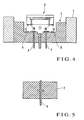
- a sensor chip 23 is mounted on a cylindrical glass base 22 in a cylindrical metal package 21 sealed by a corrosion-resistant diaphragm 24, and a sealed liquid 25 such as silicone oil is sealed in the metal package 21.
- the pressure is transmitted to the sensor chip 23 by this structure.
- the electrical connection between the sensor chip 23 and the outside is realized by connecting electrode extraction pins 26 hermetically sealed with glass and electrodes formed on the upper surface of the sensor chip 23 with wires 27.
- the sealed liquid may be eliminated.
- corrosion of the sensor chip and physical impact applied to the sensor chip pose problems. For this reason, electrodes and wires cannot be formed on the upper surface of the chip, and the electrodes are extracted from the lower side of the sensor chip.
- the electrodes cannot be extracted from the lower side of the sensor chip. More specifically, when the sensor chip extends to the lower surface of the metal package and the electrodes are extracted from the lower side of the sensor chip, stress is likely to occur in the bonding portion between the sensor chip and the seal surface of the package. For this reason, the diaphragm of the sensor chip needs to be set away from the seal surface, leading to an increase in size of the sensor.
- the measuring method shown in Fig. 6 realizes this by mounting the sensor chip 23 on the glass base 22 and bonding the glass base 22 to the metal package 21. With this method, the number of manufacturing steps increases. Also, the number of bonding surfaces increases, thereby degrading the yield.
- a sensor comprises a cylindrical sensor package, a cylindrical glass base hermetically bonded only on its perimeter is a state filled to an inner surface of the sensor package to close a space in the sensor package, a sensor chip mounted on the glass base and having electrodes and a metal bonding portion on a surface thereof opposing the glass base, the bonding portion being die-bonded to a surface of the glass base, and lead members arranged to oppose the electrodes and buried to extend through the glass base, one end of each of the lead members exposed from the surface of the glass surface being electrically bonded to a corresponding one of the electrodes.
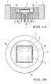
- Fig. 1A shows a pressure sensor according to an embodiment of the present invention
- Fig. 1B shows the pressure sensor shown in Fig. 1A
- a cylindrical sensor package 1 is made of corrosion-resistant metal such as stainless steel.
- a thick disk-like glass base 2 is fitted on the inner wall of the sensor package 1.
- the glass base 2 has a square recess 2a at its central portion, and a support 2b on the bottom surface of the recess 2a to support a sensor chip (to be described later).
- a sensor chip 3 is mounted on the support 2b of the glass base 2.
- Electrode extraction pins (to be referred to as electrode pins hereinafter) 4 are buried in the glass base 2 to extend through the support 2b, and serve as lead members.
- a metal plate 5 is buried slightly inside the support 2b of the glass base 2 to correspond to the periphery of the sensor chip 3.
- An atmospheric pressure introduction pipe 6 is buried in the glass base 2 to extend through the central portion of the support 2b.
- the electrode pins 4 respectively have heads 4a to be exposed from the support 2b of the glass base 2.
- the metal plate 5 is made of an Fe-Cr alloy, Fe-Ni-Cr alloy, Fe-Ni alloy, Fe-Ni-Co alloy, Ni-group alloy, or the like, and forms a square frame.
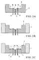
- a method of manufacturing the pressure sensor described above will be described with reference to Figs. 2A to 2C, Figs. 3A to 3F, and Fig. 4. First, how to fabricate the package on which the sensor chip 3 is to be mounted will be described.
- the thick disk-like (bottomed cylindrical) glass base 2 with a recess 2a is molded.
- the electrode pins 4, the metal plate 5 having the square shape, and the atmospheric pressure introduction pipe 6 are buried in the support 2b of the glass base 2 by integral molding.
- the electrode pins 4 are buried such that their heads 4a are exposed from the support 2b of the glass base 2 and their distal ends project from the lower side of the glass base 2.
- the glass base 2 is inserted in the sensor package 1 and heated.
- the glass base 2 is thus fused so that it is hermetically bonded to the sensor package 1.
- solder coating is performed to form solder portions 7 on the heads 4a of the electrode pins 4 and the metal plate 5. Fabrication of the sensor package 1 is ended in this manner.
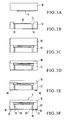
- a conductive thin film is formed on the lower surface of a sapphire first substrate 10 on the diaphragm side and patterned to form a movable electrode 11 with a predetermined shape.
- a recess 13 is formed in the center of the upper surface of a sapphire second substrate 12 by wet or dry etching, and through holes 14 for electrode leads are formed in the recess 13, so that the recess 13 and the outside communicate with each other through the through holes 14.
- a conductive thin film is formed at the center of the bottom surface of the recess 13 and patterned to form a stationary electrode 15 with a predetermined shape.
- the conductive thin films on the substrates 10 and 12 can be formed by CVD (Chemical Vapor Deposition), vacuum deposition, sputtering, or the like.
- the first and second substrates 10 and 12 are overlaid in tight contact with each other, are loaded in a vacuum furnace, and are heated in vacuum, so that they are tightly bonded to each other.
- the first substrate 10 is polished to a predetermined thickness to form a diaphragm. This diaphragm surface may be formed by etching back the first substrate 10 in accordance with wet etching, dry etching, or the like.
- a bonding portion 16 comprised of a metal film is formed along the periphery of the lower surface of the second substrate 12 by vacuum deposition to have a square frame-like shape.
- solder coating is performed to form a solder portion 17 on the bonding portion 16. During solder coating, solder also fills the through holes 14, so that electrodes 18 connected to the movable electrode 11 and electrodes 19 connected tc the stationary electrode 15 are formed inside the bonding portion 16.
- the bonding portion 16 need not form a square frame, but a plurality of bonding portions 16 may be formed at predetermined intervals.
- preplaced brazing in a solder furnace is performed. In this manner, fabrication of the sensor chip 3 is ended.
- the sensor chip 3 and glass base 2 are aligned such that the bonding portion 16 of the sensor chip 3, and the electrodes 18 and 19 of the sensor chip 3 substantially, respectively oppose the metal plate 5 of the glass base 2 and the heads 4a of the electrode pins 4 of the glass base 2.
- the aligned sensor chip 3 is placed on the glass base 2.
- the sensor chip 3 and glass base 2 are then heated to fuse solder, thereby soldering them with each other. In this manner, fabrication of the pressure sensor is ended.
- the glass base 2 is seal-bonded to the inner wall of the sensor package 1 to close the space in the sensor package 1, heat stress from the sensor package 1 can be canceled by the whole glass base 2. Since the electrode pins 4 are buried during fabrication of the glass base 2, the electrodes 18 and 19 of the sensor chip 3 can be connected to the heads 4a of the electrode pins 4 by only fixing the sensor chip 3 to the glass base 2.
- the number of manufacturing steps increases by one. According to the above embodiment, since the electrode pins 4 and metal plate 5 are buried in the glass base 2 by integral molding during fabrication of the glass base 2, the number of steps does not increase.
- the distances d1 and d2 between the electrode extraction pins, and the insulating distance cannot be decreased.
- this conventional problem does not exist basically, and the pressure sensor can be downsized.
- this electrical bond may be attained by brazing or conductive glass bonding. While soldering is performed for die bonding of the bonding portion 16 and the surface of the glass base 2, this die bonding may be attained by brazing or glass encapsulation. To fix the sensor chip 3 and to extract the electrodes simultaneously, electrical bonding and die bonding described above must be performed in accordance with the same bonding method. When the metal plate 5 is to be buried in the surface of the glass base 2 opposing the bonding portion 16, it can be achieved by only soldering and brazing among the bonding methods described above.
- the material of the glass base 2 includes sapphire glass.
- the electrode extraction pins and electrodes are bonded by soldering, and the bonding portion and the surface of the glass base are bonded by soldering, so that the sensor chip can be fixed and the electrodes can be extracted simultaneously.
- the manufacturing steps are simplified, thereby improving the yield.
- the resultant pressure sensor can be more downsized than a conventional pressure sensor in which electrode extraction pins are fixed to a metal sensor package with a glass hermetic seal. Since the center-collared pins can be used as the electrode extraction pins, a higher pressure resistance of the pins can be ensured in the longitudinal direction, largely contributing to an increase in pressure resistance of the package.
- the electrode extraction pins and the metal plate can be buried simultaneously during molding of the glass base, no soldering metallizing portion need be formed on the glass base, and the number of manufacturing steps does not increase. Also, a larger fixing force than that obtained by metallizing can be expected.
Applications Claiming Priority (2)
| Application Number | Priority Date | Filing Date | Title |
|---|---|---|---|
| JP20369699 | 1999-07-16 | ||
| JP20369699A JP3619065B2 (ja) | 1999-07-16 | 1999-07-16 | 圧力センサ |
Publications (3)
| Publication Number | Publication Date |
|---|---|
| EP1069419A2 EP1069419A2 (en) | 2001-01-17 |
| EP1069419A3 EP1069419A3 (en) | 2004-03-31 |
| EP1069419B1 true EP1069419B1 (en) | 2007-01-03 |
Family
ID=16478342
Family Applications (1)
| Application Number | Title | Priority Date | Filing Date |
|---|---|---|---|
| EP00250241A Expired - Lifetime EP1069419B1 (en) | 1999-07-16 | 2000-07-15 | Pressure sensor and method of manufacturing the same |
Country Status (6)
| Country | Link |
|---|---|
| US (1) | US6450039B1 (zh) |
| EP (1) | EP1069419B1 (zh) |
| JP (1) | JP3619065B2 (zh) |
| KR (1) | KR100372340B1 (zh) |
| CN (1) | CN1125975C (zh) |
| DE (1) | DE60032676T2 (zh) |
Cited By (2)
| Publication number | Priority date | Publication date | Assignee | Title |
|---|---|---|---|---|
| US10549982B2 (en) | 2016-02-15 | 2020-02-04 | Stmicroelectronics S.R.L. | Pressure sensor encapsulated in elastomeric material, and system including the pressure sensor |
| CN112798157A (zh) * | 2020-12-28 | 2021-05-14 | 西安赛尔电子材料科技有限公司 | 一种压力传感器基座及其制作方法 |
Families Citing this family (33)
| Publication number | Priority date | Publication date | Assignee | Title |
|---|---|---|---|---|
| DE10134360A1 (de) * | 2001-07-14 | 2003-02-06 | Endress & Hauser Gmbh & Co Kg | Drucksensor |
| JP2003045903A (ja) * | 2001-08-01 | 2003-02-14 | Fujitsu Ten Ltd | ダイボンド装置 |
| KR100411475B1 (ko) * | 2001-09-24 | 2003-12-18 | 주식회사코닉스 | 정전 용량식 압력센서의 제조방법 및 이를 이용한 압력검출 장치 |
| US6907789B2 (en) * | 2002-05-06 | 2005-06-21 | Honeywell International Inc. | Sensor package |
| EP1707931B1 (en) | 2005-03-31 | 2013-03-27 | STMicroelectronics Srl | Analog data-input device provided with a microelectromechanical pressure sensor |
| US20070013014A1 (en) * | 2005-05-03 | 2007-01-18 | Shuwen Guo | High temperature resistant solid state pressure sensor |
| US7628309B1 (en) | 2005-05-03 | 2009-12-08 | Rosemount Aerospace Inc. | Transient liquid phase eutectic bonding |
| US7538401B2 (en) * | 2005-05-03 | 2009-05-26 | Rosemount Aerospace Inc. | Transducer for use in harsh environments |
| US7183620B2 (en) * | 2005-06-21 | 2007-02-27 | Kulite Semiconductor Products, Inc. | Moisture resistant differential pressure sensors |
| EP1762925B1 (en) * | 2005-09-09 | 2016-12-21 | STMicroelectronics Srl | Analog input device with integrated pressure sensor and electronic apparatus equipped with said input device. |
| JP5139766B2 (ja) * | 2007-10-15 | 2013-02-06 | 日本電波工業株式会社 | 圧電デバイス及び圧電デバイスの製造方法 |
| KR101447114B1 (ko) * | 2008-12-30 | 2014-10-06 | 삼성전자주식회사 | 접촉힘 센서 패키지 |
| JP2010217170A (ja) * | 2009-02-17 | 2010-09-30 | Seiko Epson Corp | 複合センサー、電子機器 |
| US7921721B2 (en) * | 2009-04-09 | 2011-04-12 | Kulite Semiconductor Products, Inc. | Leadless oil filled pressure transducer |
| US8209857B2 (en) * | 2009-06-19 | 2012-07-03 | The Regents Of The University Of Michigan | Method of making a thin film device |
| US8237171B2 (en) * | 2010-02-09 | 2012-08-07 | Microsemi Corporation | High voltage high package pressure semiconductor package |
| US8587107B2 (en) * | 2010-02-09 | 2013-11-19 | Microsemi Corporation | Silicon carbide semiconductor |
| US8141429B2 (en) | 2010-07-30 | 2012-03-27 | Rosemount Aerospace Inc. | High temperature capacitive static/dynamic pressure sensors and methods of making the same |
| KR101247744B1 (ko) | 2011-04-28 | 2013-03-26 | (주)에스팩솔루션 | 몰딩형 반도체 압력센서모듈 제조방법 |
| EP2579013A1 (de) * | 2011-10-07 | 2013-04-10 | Technische Universität Darmstadt | Erfindung betreffend druckbeaufschlagte Stromdurchführungen |
| US8516897B1 (en) * | 2012-02-21 | 2013-08-27 | Honeywell International Inc. | Pressure sensor |
| US20140319677A1 (en) * | 2012-06-08 | 2014-10-30 | Hoya Corporation Usa | Submount for electronic, optoelectronic, optical, or photonic components |
| US9046426B1 (en) * | 2012-06-15 | 2015-06-02 | The United States Of America As Represented By The Administrator Of National Aeronautics And Space Administration | Modular apparatus and method for attaching multiple devices |
| US8943895B2 (en) | 2012-09-07 | 2015-02-03 | Dynisco Instruments Llc | Capacitive pressure sensor |
| US8984952B2 (en) | 2012-09-07 | 2015-03-24 | Dynisco Instruments Llc | Capacitive pressure sensor |
| US9103738B2 (en) | 2012-09-07 | 2015-08-11 | Dynisco Instruments Llc | Capacitive pressure sensor with intrinsic temperature compensation |
| US9557237B2 (en) * | 2013-11-18 | 2017-01-31 | Sensata Technologies, Inc. | MEMS pressure sensor field shield layout for surface charge immunity in oil filled packaging |
| US9316552B2 (en) * | 2014-02-28 | 2016-04-19 | Measurement Specialties, Inc. | Differential pressure sensing die |
| CN106687804A (zh) * | 2014-07-24 | 2017-05-17 | 斯佩克传感器有限责任公司 | 电化学传感器和封装以及相关方法 |
| WO2017019549A1 (en) * | 2015-07-24 | 2017-02-02 | Spec Sensors, Llc | Electrochemical sensors and packaging and related methods |
| CN106323539B (zh) * | 2016-09-23 | 2022-07-22 | 上海立格仪表有限公司 | 一种传感器基座 |
| IT201700073763A1 (it) * | 2017-07-05 | 2019-01-05 | St Microelectronics Srl | Sensore capacitivo di pressione per il monitoraggio di strutture edilizie, in particolare di calcestruzzo |
| US11435249B2 (en) * | 2018-06-12 | 2022-09-06 | Dwyer Instruments, Inc. | Electrostatic discharge resistant pressure sensor |
Family Cites Families (6)
| Publication number | Priority date | Publication date | Assignee | Title |
|---|---|---|---|---|
| US4665754A (en) * | 1985-04-08 | 1987-05-19 | Honeywell Inc. | Pressure transducer |
| US4703658A (en) * | 1986-06-18 | 1987-11-03 | Motorola, Inc. | Pressure sensor assembly |
| DE4040821A1 (de) * | 1990-12-20 | 1992-06-25 | Bosch Gmbh Robert | Elektronisches bauelement und verfahren zu dessen aufbau |
| US5581226A (en) * | 1994-11-02 | 1996-12-03 | Motorola, Inc. | High pressure sensor structure and method |
| JPH10325772A (ja) * | 1997-05-27 | 1998-12-08 | Nissan Motor Co Ltd | 半導体圧力センサおよびその製造方法 |
| JPH1164137A (ja) * | 1997-08-25 | 1999-03-05 | Hitachi Ltd | 半導体圧力センサ |
-
1999
- 1999-07-16 JP JP20369699A patent/JP3619065B2/ja not_active Expired - Lifetime
-
2000
- 2000-07-10 US US09/613,820 patent/US6450039B1/en not_active Expired - Lifetime
- 2000-07-14 KR KR10-2000-0040588A patent/KR100372340B1/ko not_active IP Right Cessation
- 2000-07-14 CN CN00120256A patent/CN1125975C/zh not_active Expired - Fee Related
- 2000-07-15 EP EP00250241A patent/EP1069419B1/en not_active Expired - Lifetime
- 2000-07-15 DE DE60032676T patent/DE60032676T2/de not_active Expired - Lifetime
Cited By (3)
| Publication number | Priority date | Publication date | Assignee | Title |
|---|---|---|---|---|
| US10549982B2 (en) | 2016-02-15 | 2020-02-04 | Stmicroelectronics S.R.L. | Pressure sensor encapsulated in elastomeric material, and system including the pressure sensor |
| US11254561B2 (en) | 2016-02-15 | 2022-02-22 | Stmicroelectronics S.R.L. | Pressure sensor encapsulated in elastomeric material, and system including the pressure sensor |
| CN112798157A (zh) * | 2020-12-28 | 2021-05-14 | 西安赛尔电子材料科技有限公司 | 一种压力传感器基座及其制作方法 |
Also Published As
| Publication number | Publication date |
|---|---|
| DE60032676D1 (de) | 2007-02-15 |
| CN1125975C (zh) | 2003-10-29 |
| KR20010029946A (ko) | 2001-04-16 |
| EP1069419A2 (en) | 2001-01-17 |
| JP3619065B2 (ja) | 2005-02-09 |
| US6450039B1 (en) | 2002-09-17 |
| EP1069419A3 (en) | 2004-03-31 |
| CN1281140A (zh) | 2001-01-24 |
| JP2001033329A (ja) | 2001-02-09 |
| DE60032676T2 (de) | 2007-11-08 |
| KR100372340B1 (ko) | 2003-02-17 |
Similar Documents
| Publication | Publication Date | Title |
|---|---|---|
| EP1069419B1 (en) | Pressure sensor and method of manufacturing the same | |
| US5801313A (en) | Capacitive sensor | |
| US4838088A (en) | Pressure transducer and method for fabricating same | |
| EP1860417B1 (en) | A pressure sensor having a chamber and a method for fabricating the same | |
| US7057247B2 (en) | Combined absolute differential transducer | |
| US7080560B2 (en) | Semiconductor pressure sensor | |
| US5344523A (en) | Overpressure-protected, polysilicon, capacitive differential pressure sensor and method of making the same | |
| US8230746B2 (en) | Combined type pressure gauge, and manufacturing method of combined type pressure gauge | |
| JPH0533732B2 (zh) | ||
| US20070275495A1 (en) | Method for fabricating a pressure sensor using SOI wafers | |
| JPS62500545A (ja) | 脆性ダイヤフラムを使用した圧力感知セル | |
| US8181530B2 (en) | Leadless oil filled pressure transducer | |
| JPS61176832A (ja) | トランスジユーサ・インサート、その製造方法、および機械的変動測定センサ | |
| EP2873958B1 (en) | Capacitive pressure sensors for high temperature applications | |
| JP4539413B2 (ja) | 静電容量型センサの構造 | |
| JP3316555B2 (ja) | 圧力センサ | |
| KR100636823B1 (ko) | Mems 소자 패키지 및 그 제조방법 | |
| JP2002267559A (ja) | 静電容量式圧力センサ、センサ素子およびセンサ素子の製造方法 | |
| JP2519393B2 (ja) | 半導体力学量センサの製造方法 | |
| CN113447171B (zh) | 一种压力计芯片及其制造工艺 | |
| JPH08254474A (ja) | 半導体式センサ | |
| CN113465794B (zh) | 一种双空腔压力计芯片及其制造工艺 | |
| US6236095B1 (en) | Carrier structure for semiconductor transducers | |
| JPH1022512A (ja) | 静電容量型圧力センサ | |
| CN115594145A (zh) | 电容式压力传感器及其制作方法 |
Legal Events
| Date | Code | Title | Description |
|---|---|---|---|
| PUAI | Public reference made under article 153(3) epc to a published international application that has entered the european phase |
Free format text: ORIGINAL CODE: 0009012 |
|
| AK | Designated contracting states |
Kind code of ref document: A2 Designated state(s): AT BE CH CY DE DK ES FI FR GB GR IE IT LI LU MC NL PT SE |
|
| AX | Request for extension of the european patent |
Free format text: AL;LT;LV;MK;RO;SI |
|
| PUAL | Search report despatched |
Free format text: ORIGINAL CODE: 0009013 |
|
| AK | Designated contracting states |
Kind code of ref document: A3 Designated state(s): AT BE CH CY DE DK ES FI FR GB GR IE IT LI LU MC NL PT SE |
|
| AX | Request for extension of the european patent |
Extension state: AL LT LV MK RO SI |
|
| RIC1 | Information provided on ipc code assigned before grant |
Ipc: 7G 01L 9/12 A Ipc: 7G 01L 9/04 B Ipc: 7G 01L 9/00 B |
|
| 17P | Request for examination filed |
Effective date: 20040527 |
|
| AKX | Designation fees paid |
Designated state(s): DE FR GB NL |
|
| GRAP | Despatch of communication of intention to grant a patent |
Free format text: ORIGINAL CODE: EPIDOSNIGR1 |
|
| GRAS | Grant fee paid |
Free format text: ORIGINAL CODE: EPIDOSNIGR3 |
|
| GRAA | (expected) grant |
Free format text: ORIGINAL CODE: 0009210 |
|
| AK | Designated contracting states |
Kind code of ref document: B1 Designated state(s): DE FR GB NL |
|
| PG25 | Lapsed in a contracting state [announced via postgrant information from national office to epo] |
Ref country code: NL Free format text: LAPSE BECAUSE OF FAILURE TO SUBMIT A TRANSLATION OF THE DESCRIPTION OR TO PAY THE FEE WITHIN THE PRESCRIBED TIME-LIMIT Effective date: 20070103 |
|
| REG | Reference to a national code |
Ref country code: GB Ref legal event code: FG4D |
|
| REF | Corresponds to: |
Ref document number: 60032676 Country of ref document: DE Date of ref document: 20070215 Kind code of ref document: P |
|
| ET | Fr: translation filed | ||
| NLV1 | Nl: lapsed or annulled due to failure to fulfill the requirements of art. 29p and 29m of the patents act | ||
| PLBE | No opposition filed within time limit |
Free format text: ORIGINAL CODE: 0009261 |
|
| STAA | Information on the status of an ep patent application or granted ep patent |
Free format text: STATUS: NO OPPOSITION FILED WITHIN TIME LIMIT |
|
| 26N | No opposition filed |
Effective date: 20071005 |
|
| REG | Reference to a national code |
Ref country code: FR Ref legal event code: PLFP Year of fee payment: 17 |
|
| REG | Reference to a national code |
Ref country code: FR Ref legal event code: PLFP Year of fee payment: 18 |
|
| PGFP | Annual fee paid to national office [announced via postgrant information from national office to epo] |
Ref country code: FR Payment date: 20170613 Year of fee payment: 18 |
|
| PGFP | Annual fee paid to national office [announced via postgrant information from national office to epo] |
Ref country code: GB Payment date: 20170712 Year of fee payment: 18 Ref country code: DE Payment date: 20170711 Year of fee payment: 18 |
|
| REG | Reference to a national code |
Ref country code: DE Ref legal event code: R119 Ref document number: 60032676 Country of ref document: DE |
|
| GBPC | Gb: european patent ceased through non-payment of renewal fee |
Effective date: 20180715 |
|
| PG25 | Lapsed in a contracting state [announced via postgrant information from national office to epo] |
Ref country code: GB Free format text: LAPSE BECAUSE OF NON-PAYMENT OF DUE FEES Effective date: 20180715 Ref country code: DE Free format text: LAPSE BECAUSE OF NON-PAYMENT OF DUE FEES Effective date: 20190201 Ref country code: FR Free format text: LAPSE BECAUSE OF NON-PAYMENT OF DUE FEES Effective date: 20180731 |