EP1069206A2 - Leitende Verbinder im Nanobereich und ihr Herstellungsverfahren - Google Patents
Leitende Verbinder im Nanobereich und ihr Herstellungsverfahren Download PDFInfo
- Publication number
- EP1069206A2 EP1069206A2 EP00305578A EP00305578A EP1069206A2 EP 1069206 A2 EP1069206 A2 EP 1069206A2 EP 00305578 A EP00305578 A EP 00305578A EP 00305578 A EP00305578 A EP 00305578A EP 1069206 A2 EP1069206 A2 EP 1069206A2
- Authority
- EP
- European Patent Office
- Prior art keywords
- nanoconductors
- substrate
- standing
- length
- equal length
- Prior art date
- Legal status (The legal status is an assumption and is not a legal conclusion. Google has not performed a legal analysis and makes no representation as to the accuracy of the status listed.)
- Withdrawn
Links
Images

Classifications
-
- H—ELECTRICITY
- H10—SEMICONDUCTOR DEVICES; ELECTRIC SOLID-STATE DEVICES NOT OTHERWISE PROVIDED FOR
- H10W—GENERIC PACKAGES, INTERCONNECTIONS, CONNECTORS OR OTHER CONSTRUCTIONAL DETAILS OF DEVICES COVERED BY CLASS H10
- H10W72/00—Interconnections or connectors in packages
- H10W72/20—Bump connectors, e.g. solder bumps or copper pillars; Dummy bumps; Thermal bumps
-
- B—PERFORMING OPERATIONS; TRANSPORTING
- B82—NANOTECHNOLOGY
- B82Y—SPECIFIC USES OR APPLICATIONS OF NANOSTRUCTURES; MEASUREMENT OR ANALYSIS OF NANOSTRUCTURES; MANUFACTURE OR TREATMENT OF NANOSTRUCTURES
- B82Y10/00—Nanotechnology for information processing, storage or transmission, e.g. quantum computing or single electron logic
-
- B—PERFORMING OPERATIONS; TRANSPORTING
- B82—NANOTECHNOLOGY
- B82Y—SPECIFIC USES OR APPLICATIONS OF NANOSTRUCTURES; MEASUREMENT OR ANALYSIS OF NANOSTRUCTURES; MANUFACTURE OR TREATMENT OF NANOSTRUCTURES
- B82Y30/00—Nanotechnology for materials or surface science, e.g. nanocomposites
-
- C—CHEMISTRY; METALLURGY
- C30—CRYSTAL GROWTH
- C30B—SINGLE-CRYSTAL GROWTH; UNIDIRECTIONAL SOLIDIFICATION OF EUTECTIC MATERIAL OR UNIDIRECTIONAL DEMIXING OF EUTECTOID MATERIAL; REFINING BY ZONE-MELTING OF MATERIAL; PRODUCTION OF A HOMOGENEOUS POLYCRYSTALLINE MATERIAL WITH DEFINED STRUCTURE; SINGLE CRYSTALS OR HOMOGENEOUS POLYCRYSTALLINE MATERIAL WITH DEFINED STRUCTURE; AFTER-TREATMENT OF SINGLE CRYSTALS OR A HOMOGENEOUS POLYCRYSTALLINE MATERIAL WITH DEFINED STRUCTURE; APPARATUS THEREFOR
- C30B25/00—Single-crystal growth by chemical reaction of reactive gases, e.g. chemical vapour-deposition growth
-
- C—CHEMISTRY; METALLURGY
- C30—CRYSTAL GROWTH
- C30B—SINGLE-CRYSTAL GROWTH; UNIDIRECTIONAL SOLIDIFICATION OF EUTECTIC MATERIAL OR UNIDIRECTIONAL DEMIXING OF EUTECTOID MATERIAL; REFINING BY ZONE-MELTING OF MATERIAL; PRODUCTION OF A HOMOGENEOUS POLYCRYSTALLINE MATERIAL WITH DEFINED STRUCTURE; SINGLE CRYSTALS OR HOMOGENEOUS POLYCRYSTALLINE MATERIAL WITH DEFINED STRUCTURE; AFTER-TREATMENT OF SINGLE CRYSTALS OR A HOMOGENEOUS POLYCRYSTALLINE MATERIAL WITH DEFINED STRUCTURE; APPARATUS THEREFOR
- C30B29/00—Single crystals or homogeneous polycrystalline material with defined structure characterised by the material or by their shape
- C30B29/60—Single crystals or homogeneous polycrystalline material with defined structure characterised by the material or by their shape characterised by shape
- C30B29/605—Products containing multiple oriented crystallites, e.g. columnar crystallites
-
- H—ELECTRICITY
- H10—SEMICONDUCTOR DEVICES; ELECTRIC SOLID-STATE DEVICES NOT OTHERWISE PROVIDED FOR
- H10P—GENERIC PROCESSES OR APPARATUS FOR THE MANUFACTURE OR TREATMENT OF DEVICES COVERED BY CLASS H10
- H10P14/00—Formation of materials, e.g. in the shape of layers or pillars
- H10P14/40—Formation of materials, e.g. in the shape of layers or pillars of conductive or resistive materials
- H10P14/46—Formation of materials, e.g. in the shape of layers or pillars of conductive or resistive materials using a liquid
-
- H—ELECTRICITY
- H10—SEMICONDUCTOR DEVICES; ELECTRIC SOLID-STATE DEVICES NOT OTHERWISE PROVIDED FOR
- H10W—GENERIC PACKAGES, INTERCONNECTIONS, CONNECTORS OR OTHER CONSTRUCTIONAL DETAILS OF DEVICES COVERED BY CLASS H10
- H10W20/00—Interconnections in chips, wafers or substrates
- H10W20/01—Manufacture or treatment
- H10W20/031—Manufacture or treatment of conductive parts of the interconnections
-
- H—ELECTRICITY
- H10—SEMICONDUCTOR DEVICES; ELECTRIC SOLID-STATE DEVICES NOT OTHERWISE PROVIDED FOR
- H10W—GENERIC PACKAGES, INTERCONNECTIONS, CONNECTORS OR OTHER CONSTRUCTIONAL DETAILS OF DEVICES COVERED BY CLASS H10
- H10W72/00—Interconnections or connectors in packages
-
- H—ELECTRICITY
- H10—SEMICONDUCTOR DEVICES; ELECTRIC SOLID-STATE DEVICES NOT OTHERWISE PROVIDED FOR
- H10W—GENERIC PACKAGES, INTERCONNECTIONS, CONNECTORS OR OTHER CONSTRUCTIONAL DETAILS OF DEVICES COVERED BY CLASS H10
- H10W72/00—Interconnections or connectors in packages
- H10W72/071—Connecting or disconnecting
- H10W72/075—Connecting or disconnecting of bond wires
-
- H—ELECTRICITY
- H10—SEMICONDUCTOR DEVICES; ELECTRIC SOLID-STATE DEVICES NOT OTHERWISE PROVIDED FOR
- H10W—GENERIC PACKAGES, INTERCONNECTIONS, CONNECTORS OR OTHER CONSTRUCTIONAL DETAILS OF DEVICES COVERED BY CLASS H10
- H10W72/00—Interconnections or connectors in packages
- H10W72/20—Bump connectors, e.g. solder bumps or copper pillars; Dummy bumps; Thermal bumps
- H10W72/251—Materials
-
- H—ELECTRICITY
- H10—SEMICONDUCTOR DEVICES; ELECTRIC SOLID-STATE DEVICES NOT OTHERWISE PROVIDED FOR
- H10W—GENERIC PACKAGES, INTERCONNECTIONS, CONNECTORS OR OTHER CONSTRUCTIONAL DETAILS OF DEVICES COVERED BY CLASS H10
- H10W72/00—Interconnections or connectors in packages
- H10W72/50—Bond wires
- H10W72/551—Materials of bond wires
- H10W72/552—Materials of bond wires comprising metals or metalloids, e.g. silver
- H10W72/5522—Materials of bond wires comprising metals or metalloids, e.g. silver comprising gold [Au]
-
- Y—GENERAL TAGGING OF NEW TECHNOLOGICAL DEVELOPMENTS; GENERAL TAGGING OF CROSS-SECTIONAL TECHNOLOGIES SPANNING OVER SEVERAL SECTIONS OF THE IPC; TECHNICAL SUBJECTS COVERED BY FORMER USPC CROSS-REFERENCE ART COLLECTIONS [XRACs] AND DIGESTS
- Y10—TECHNICAL SUBJECTS COVERED BY FORMER USPC
- Y10S—TECHNICAL SUBJECTS COVERED BY FORMER USPC CROSS-REFERENCE ART COLLECTIONS [XRACs] AND DIGESTS
- Y10S977/00—Nanotechnology
- Y10S977/70—Nanostructure
- Y10S977/701—Integrated with dissimilar structures on a common substrate
- Y10S977/72—On an electrically conducting, semi-conducting, or semi-insulating substrate
-
- Y—GENERAL TAGGING OF NEW TECHNOLOGICAL DEVELOPMENTS; GENERAL TAGGING OF CROSS-SECTIONAL TECHNOLOGIES SPANNING OVER SEVERAL SECTIONS OF THE IPC; TECHNICAL SUBJECTS COVERED BY FORMER USPC CROSS-REFERENCE ART COLLECTIONS [XRACs] AND DIGESTS
- Y10—TECHNICAL SUBJECTS COVERED BY FORMER USPC
- Y10S—TECHNICAL SUBJECTS COVERED BY FORMER USPC CROSS-REFERENCE ART COLLECTIONS [XRACs] AND DIGESTS
- Y10S977/00—Nanotechnology
- Y10S977/70—Nanostructure
- Y10S977/734—Fullerenes, i.e. graphene-based structures, such as nanohorns, nanococoons, nanoscrolls or fullerene-like structures, e.g. WS2 or MoS2 chalcogenide nanotubes, planar C3N4, etc.
- Y10S977/742—Carbon nanotubes, CNTs
- Y10S977/745—Carbon nanotubes, CNTs having a modified surface
-
- Y—GENERAL TAGGING OF NEW TECHNOLOGICAL DEVELOPMENTS; GENERAL TAGGING OF CROSS-SECTIONAL TECHNOLOGIES SPANNING OVER SEVERAL SECTIONS OF THE IPC; TECHNICAL SUBJECTS COVERED BY FORMER USPC CROSS-REFERENCE ART COLLECTIONS [XRACs] AND DIGESTS
- Y10—TECHNICAL SUBJECTS COVERED BY FORMER USPC
- Y10S—TECHNICAL SUBJECTS COVERED BY FORMER USPC CROSS-REFERENCE ART COLLECTIONS [XRACs] AND DIGESTS
- Y10S977/00—Nanotechnology
- Y10S977/70—Nanostructure
- Y10S977/762—Nanowire or quantum wire, i.e. axially elongated structure having two dimensions of 100 nm or less
-
- Y—GENERAL TAGGING OF NEW TECHNOLOGICAL DEVELOPMENTS; GENERAL TAGGING OF CROSS-SECTIONAL TECHNOLOGIES SPANNING OVER SEVERAL SECTIONS OF THE IPC; TECHNICAL SUBJECTS COVERED BY FORMER USPC CROSS-REFERENCE ART COLLECTIONS [XRACs] AND DIGESTS
- Y10—TECHNICAL SUBJECTS COVERED BY FORMER USPC
- Y10S—TECHNICAL SUBJECTS COVERED BY FORMER USPC CROSS-REFERENCE ART COLLECTIONS [XRACs] AND DIGESTS
- Y10S977/00—Nanotechnology
- Y10S977/84—Manufacture, treatment, or detection of nanostructure
- Y10S977/842—Manufacture, treatment, or detection of nanostructure for carbon nanotubes or fullerenes
- Y10S977/843—Gas phase catalytic growth, i.e. chemical vapor deposition
-
- Y—GENERAL TAGGING OF NEW TECHNOLOGICAL DEVELOPMENTS; GENERAL TAGGING OF CROSS-SECTIONAL TECHNOLOGIES SPANNING OVER SEVERAL SECTIONS OF THE IPC; TECHNICAL SUBJECTS COVERED BY FORMER USPC CROSS-REFERENCE ART COLLECTIONS [XRACs] AND DIGESTS
- Y10—TECHNICAL SUBJECTS COVERED BY FORMER USPC
- Y10S—TECHNICAL SUBJECTS COVERED BY FORMER USPC CROSS-REFERENCE ART COLLECTIONS [XRACs] AND DIGESTS
- Y10S977/00—Nanotechnology
- Y10S977/902—Specified use of nanostructure
- Y10S977/932—Specified use of nanostructure for electronic or optoelectronic application
Definitions
- This invention relates to conductive connecting elements and, in particular, to nanoscale connectors for microdevices such as integrated circuit components and to methods for making such connectors.
- nanoscale connectors particularly useful for connecting microscale devices comprise free-standing nanoscale conductors.
- the nanoscale conductors are conveniently fabricated in sets of controlled, preferably equal length by providing a removable substrate, growing conductive nanotubes or nanowires on the substrate, equalizing the length of the nanoscale conductors, and removing the substrate.
- the removable substrate is soluble, leaving a collection of free standing nanoscale connectors in suspension or solution.
- Part I describes the conventional growth of substrate-supported nanoscale conductors.
- Part II describes the fabrication of free-standing nanoscale conductive connectors; and
- Part III describes the use of nanoscale conductive connectors.
- Nanoconductors are tiny conductive tubes (hollow) or wires (solid) with a very small size scale of the order of 1.0-100 nanometers in diameter and 0.5-10 ⁇ m in length. Carbon nanotubes are representative. Their structure and fabrication are reported in J. Liu et al., Science , Vol. 280, p. 1253 (1998); Z. F. Ren et al., Science , Vol. 282, p. 1105 (1998); W. Z. Li , et al., Science , Vol. 274, p. 1701 (1996); S.
- Carbon nanotubes exhibit unique atomic arrangements, having useful physical properties such as one-dimensional electrical behavior, quantum conductance, and ballistic electron transport.
- the ballistic transport in carbon nanotubes permits the passage of huge electrical currents, with the magnitude of current density comparable to or better than those in superconductors.
- Carbon nanotubes are among the smallest dimensioned nanotubes materials with generally high aspect ratio and small diameter of about ⁇ 1.0 nm in the case of single-wall nanotubes and less than ⁇ 50 nm in the case of multi-wall nanotubes. See A. G. Rinzler et al, Applied Physics , Vol. A67, p. 29 (1998); Kiang et al, J. Physical Chemistry , Vol. 98, p. 6612, (1994); and Kiang et al, Physical Review Letters , Vol. 81, p. 1869 (1998), which are incorporated herein by reference.
- High-quality single-walled carbon nanotubes are typically grown as randomly oriented, needle-like or spaghetti-like, tangled tubules. They can be grown by chemical vapor deposition (CVD), laser ablation or electric arc growth. CVD methods such as used by Ren et al., Fan et al., and Li et al can produce multiwall nanotubes attached onto a substrate, often with aligned, parallel growth perpendicular to the substrate. Carbon nanotubes are grown on a substrate by catalytic decomposition of hydrocarbon-containing precursors such as ethylene, methane, or benzene.
- hydrocarbon-containing precursors such as ethylene, methane, or benzene.
- Nucleation layers such as thin coatings of Ni, Co, or Fe, are often intentionally added onto the substrate surface in order to nucleate a multiplicity of isolated nanotubes.
- Carbon nanotubes can also be nucleated and grown on a substrate without a metal nucleating layer, by using a precursor including one or more of these metal atoms. During CVD the metal atoms serve to nucleate the nanotubes on the substrate surface. See H. M. Cheng et al., Chem. Physics Letters , Vol. 289, p. 602 (1998), which is incorporated herein by reference.
- Semiconductor nanowires are grown on substrates by similar processes.
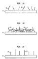
- Figs. 1(a)-(c) schematically illustrate various configurations of nanoconductors conductors 10 grown on a substrate 11.
- the nanoconductors 10 can be carbon nanotubes or Si or GaAs nanowires, synthesized by any one of a variety of methods. In the absence of alignment processing the nanoconductors tend to grow with the random orientation morphology shown in Fig. 1(a) or with the tangled growth morphology shown in Fig. 1(b). Such a tangled morphology of nanoconductors is also obtained in laser ablation synthesis.
- the nanoconductors can be grown with an aligned morphology substantially perpendicular to the substrate.
- Such aligned nanoconductors 10 are schematically illustrated in Fig. 1(c).
- Nanoscale conductive connectors for connecting microdevices should be free-standing and preferably of equal length.
- such connectors should be prepared as a collection of free-standing nanoconductors so that they can be placed and bonded for circuit interconnections. They should be of approximately equal length to avoid unwanted short circuits from connectors that are too long and unwanted open circuits from connectors that are too short.
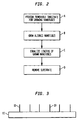
- Fig. 2 is a schematic flow diagram of the steps involved in making a collection of free-standing nanoconnectors of controlled, substantially equal length.
- the first step shown in block A of Fig. 2, is to provide a removable substrate for nanoconductor growth.
- the substrate is removable by dissolving in water or another solvent.
- the substrate can be a sodium chloride crystal or another water-soluble material.
- Acid-dissolvable metals such Cu, Ni, Co, Mo, Fe, V, Au, Ag, and their alloys, or base-dissolvable metals such as Al may also be used.
- the substrate can be made of a soluable polymer such as polyvinyl alcohol, polyvinyl acetate, polyacrylamide, acrylonitrile-butadiene-styrene.
- the removable substrate alternatively, can be a volatile (evaporable) material such as PMMA polymer.
- the removable substrate can be a layered combination of metals or compounds.
- a solvent-soluble material such as polyacrylamide or an acid-soluable metal such as Cu
- the coating can be a catalyst metal such as Ni, Fe or Co, and can be deposited as a continuous, spotly or patterned film by sputtering, vacuum evaporation or electrochemical deposition.
- the next step shown in Block B is to grow aligned nanoconductors on the removable substrate.
- aligned carbon nanotubes can be grown using CVD growth in the direction of an applied electric field, vapor concentration gradient, temperature gradient, or recessed pores in the substrate to produce aligned nanotubes as discussed in Ren et al ., Fan et al. and Li et al .
- Aligned nanoconductors 10 on a substrate 11 are schematically illustrated in Fig. 1(c).
- the average deviation from vertical growth is less than 25 degrees and preferably less than 15 degrees.
- the third step (Block C of Fig. 2) is to equalize the lengths of the grown nanoconductors. Ideally, length equality is achieved by careful growth, but equal length growth is difficult to achieve in practice.
- Fig. 3 schematically illustrates equal length, aligned nanoconductors 10 on a removable substrate 11.
- the third step of Fig. 2 can be effected by adding to the substrate a sacrificial layer of uniform thickness which will bury the nanoconductors to an equal height level while leaving exposed the nanoconductor material beyond the desired length.
- a sacrificial layer of uniform thickness which will bury the nanoconductors to an equal height level while leaving exposed the nanoconductor material beyond the desired length.
- Fig. 4 shows the nanoconductors 10 partially buried by the sacrificial layer 12.
- Such a sacrificial locking layer 12 temporarily protects the buried nanoconductor regions 10A while the exposed extra length regions 10B are removed.
- the sacrificial layer 12 is desirably a material that can be relatively easily removed after the length equalization, i.e., by dissolving in water or in a solvent, by chemically or electrochemically etching, or by vaporizing through heating.
- exemplary sacrificial layer materials include water-soluble or solvent-soluble salts such as sodium chloride, silver chloride, potassium nitrate, copper sulfate, and indium chloride, or soluble organic materials such as sugar and glucose.
- the sacrificial layer material can also be a chemically etchable metal or alloy such as Cu, Ni, Fe, Co, Mo, V, Al, Zn, In, Ag, Cu-Ni alloy, Ni-Fe alloy and others.
- the sacrificial layer 12 may also be a vaporizable material such as Zn which can be decomposed or burned away by heat.
- the sacrificial layer 12 can be added by chemical deposition such as electroplating or electroless plating, by physical vapor deposition such as sputtering, evaporation, laser ablation, ion beam deposition, or by chemical vapor decomposition.
- An advantageous method is to electroplate in an electrolyte containing the ions of a metal to be deposited, e.g., Ni from a NiSO 4 solution or Cu from a CuSO 4 -containing solution.
- the substrate 11 desirably has a catalyst metal coating 13 such as Ni, Co, or Fe.
- the electrodeposition of the metal preferentially occurs on the catalyst metal coating rather than on the nanoconductors because of chemical affinity.
- the thickness of the electroplated metal is controlled by the processing variables such as the time, temperature, electrolyte concentration, and current density.
- the thickness of the uniformly deposited sacrificial layer 12 determines the nanoconductor length.
- the desired average length (region 10A) is typically in the range of 10-10,000 nm.
- the lengths of at least 90% of the nanoconductors should not deviate more than 20% from the average length.
- the exposed portions 10B of the nanotubes are removed.
- the exposed portion can be burned away by heating in an oxidizing atmosphere at temperatures in the range of 200-1000°C for 0.1-10,000 minutes.
- the exposed portion 10B can also be removed by mechanical polishing or chemical etching so that only their buried, equal-length part 10A remains.
- Fig. 5 schematically illustrates the workpiece after removal of the exposed portions.
- the third step of Fig. 2 may also achieved by alternative methods without employing a sacrificial layer.
- equalization can be achieved by laser cutting or hot blade cutting, as disclosed in United States Patent application Serial No. 09/236,933 filed by S. Jin on January 25, 1999 and entitled "Article Comprising Aligned Truncated Carbon Nanotubes", which is incorporated herein by reference.
- the next step in the process of Fig. 2 is to remove the substrate This includes removing any sacrificial layers used in the length equalization process and any catalyst metal film added for nanoconductor nucleation. Removal is advantageously obtained by dissolving the substrate materials, and the particular solvent used depends on the materials.
- the workpiece comprising the substrate 11 and the equal height nanoconductors 10A is typically placed in a bath of solvent 14.
- the result of this step is a collection of free-standing, equal length nanoconductors. They typically have diameters averaging less than 100 nm, and the lengths of at least 90% of the nanoconductors in the collection do not deviate by more than 20 percent from the average length.
- the free-standing, equal-length nanoconductors obtained by the process of Fig. 2 are advantageously dispersed in liquid or functionalized and dissolved in liquid so that the collection remains separated without agglomeration.
- Carbon nanotubes allow various chemical modifications of their open ends, outside walls, or the tube-interior cavity by functionalization chemistry.
- single-wall carbon carbon nanotubes can be made soluble in common organic solvents such as chloroform, dichloromethane, toluene, CS 2 , chlorobenzene, etc. by attaching long-chain molecules such as octadecylamin, NH(CH 2 ) 17 CH 3 , to the open ends of the nanotubes. This can be accomplished via formation of amide functionality.
- Fig. 7 illustrates carbon nanotubes 10A modified for solution.
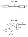
- the free-standing, equal-length dispersed nanoconductors can be applied to an electronic circuit and for interconnection and bonding. We will refer to such connectors as nanoconnectors.
- the nanoconnectors 10A can be placed on circuit pads 80 by individual micro-manipulation or nano-manipulation under high resolution microscope.
- the nanoconnectors 10A are placed by random dropping such as by sedimentation from a thin layer of solution. Because of the equal-length of the nanoconnectors without undesirably long nanoconnectors, unwanted electrical shorting is avoided.
- the nanoconnectors 10A are then dried and bonded onto the underlying pads 80, as by soldering.
- the pad surface can be pre-coated with a solder layer and heated together with the contacting nanoconnectors).
- the device surface can be washed then to remove non-bonded nanoconnectors, i.e. those in Fig. 8(b) which are sitting on the surface of the circuit device without touching any of the contact pads 80.
- the sedimentation and the solder bonding process can be repeated until all the desired electrical interconnections between adjacent contact pads are obtained.
Landscapes
- Chemical & Material Sciences (AREA)
- Engineering & Computer Science (AREA)
- Nanotechnology (AREA)
- Crystallography & Structural Chemistry (AREA)
- Materials Engineering (AREA)
- Physics & Mathematics (AREA)
- Metallurgy (AREA)
- Organic Chemistry (AREA)
- General Physics & Mathematics (AREA)
- Composite Materials (AREA)
- Condensed Matter Physics & Semiconductors (AREA)
- General Chemical & Material Sciences (AREA)
- Chemical Kinetics & Catalysis (AREA)
- Mathematical Physics (AREA)
- Theoretical Computer Science (AREA)
- Carbon And Carbon Compounds (AREA)
- Manufacture Of Metal Powder And Suspensions Thereof (AREA)
- Internal Circuitry In Semiconductor Integrated Circuit Devices (AREA)
- Wire Bonding (AREA)
Applications Claiming Priority (2)
| Application Number | Priority Date | Filing Date | Title |
|---|---|---|---|
| US09/354,928 US6322713B1 (en) | 1999-07-15 | 1999-07-15 | Nanoscale conductive connectors and method for making same |
| US354928 | 2003-01-30 |
Publications (2)
| Publication Number | Publication Date |
|---|---|
| EP1069206A2 true EP1069206A2 (de) | 2001-01-17 |
| EP1069206A3 EP1069206A3 (de) | 2001-10-31 |
Family
ID=23395489
Family Applications (1)
| Application Number | Title | Priority Date | Filing Date |
|---|---|---|---|
| EP00305578A Withdrawn EP1069206A3 (de) | 1999-07-15 | 2000-07-03 | Leitende Verbinder im Nanobereich und ihr Herstellungsverfahren |
Country Status (3)
| Country | Link |
|---|---|
| US (1) | US6322713B1 (de) |
| EP (1) | EP1069206A3 (de) |
| JP (1) | JP2001102381A (de) |
Cited By (29)
| Publication number | Priority date | Publication date | Assignee | Title |
|---|---|---|---|---|
| WO2002099845A3 (de) * | 2001-06-06 | 2003-08-21 | Infineon Technologies Ag | Elektronischer chip und elektronische chip-anordnung |
| US6706402B2 (en) | 2001-07-25 | 2004-03-16 | Nantero, Inc. | Nanotube films and articles |
| US6784028B2 (en) | 2001-12-28 | 2004-08-31 | Nantero, Inc. | Methods of making electromechanical three-trace junction devices |
| US6836424B2 (en) | 2001-07-25 | 2004-12-28 | Nantero, Inc. | Hybrid circuit having nanotube electromechanical memory |
| US6835591B2 (en) | 2001-07-25 | 2004-12-28 | Nantero, Inc. | Methods of nanotube films and articles |
| US6889216B2 (en) | 2002-03-12 | 2005-05-03 | Knowm Tech, Llc | Physical neural network design incorporating nanotechnology |
| US6911682B2 (en) | 2001-12-28 | 2005-06-28 | Nantero, Inc. | Electromechanical three-trace junction devices |
| US6919592B2 (en) | 2001-07-25 | 2005-07-19 | Nantero, Inc. | Electromechanical memory array using nanotube ribbons and method for making same |
| DE102004035368A1 (de) * | 2004-07-21 | 2006-02-16 | Infineon Technologies Ag | Substrat mit Leiterbahnen und Herstellung der Leiterbahnen auf Substraten für Halbleiterbauteile |
| US7120047B2 (en) | 2001-07-25 | 2006-10-10 | Segal Brent M | Device selection circuitry constructed with nanotube technology |
| US7176505B2 (en) | 2001-12-28 | 2007-02-13 | Nantero, Inc. | Electromechanical three-trace junction devices |
| DE102006031322A1 (de) * | 2006-07-06 | 2007-09-27 | Siemens Ag | Elektromechanisches Bauteil |
| US7335395B2 (en) | 2002-04-23 | 2008-02-26 | Nantero, Inc. | Methods of using pre-formed nanotubes to make carbon nanotube films, layers, fabrics, ribbons, elements and articles |
| DE102006041515A1 (de) * | 2006-08-28 | 2008-03-20 | Leibniz-Institut Für Festkörper- Und Werkstoffforschung Dresden E.V. | Ein- oder mehrwandige beschichtete Kohlenstoff-Nanoröhren, Verfahren zu deren Herstellung und Verwendung |
| US7392230B2 (en) | 2002-03-12 | 2008-06-24 | Knowmtech, Llc | Physical neural network liquid state machine utilizing nanotechnology |
| US7398259B2 (en) | 2002-03-12 | 2008-07-08 | Knowmtech, Llc | Training of a physical neural network |
| US7409375B2 (en) | 2005-05-23 | 2008-08-05 | Knowmtech, Llc | Plasticity-induced self organizing nanotechnology for the extraction of independent components from a data stream |
| US7412428B2 (en) | 2002-03-12 | 2008-08-12 | Knowmtech, Llc. | Application of hebbian and anti-hebbian learning to nanotechnology-based physical neural networks |
| US7420396B2 (en) | 2005-06-17 | 2008-09-02 | Knowmtech, Llc | Universal logic gate utilizing nanotechnology |
| US7426501B2 (en) | 2003-07-18 | 2008-09-16 | Knowntech, Llc | Nanotechnology neural network methods and systems |
| US7502769B2 (en) | 2005-01-31 | 2009-03-10 | Knowmtech, Llc | Fractal memory and computational methods and systems based on nanotechnology |
| US7560136B2 (en) | 2003-01-13 | 2009-07-14 | Nantero, Inc. | Methods of using thin metal layers to make carbon nanotube films, layers, fabrics, ribbons, elements and articles |
| US7566478B2 (en) | 2001-07-25 | 2009-07-28 | Nantero, Inc. | Methods of making carbon nanotube films, layers, fabrics, ribbons, elements and articles |
| US7599895B2 (en) | 2005-07-07 | 2009-10-06 | Knowm Tech, Llc | Methodology for the configuration and repair of unreliable switching elements |
| US7752151B2 (en) | 2002-06-05 | 2010-07-06 | Knowmtech, Llc | Multilayer training in a physical neural network formed utilizing nanotechnology |
| US7827131B2 (en) | 2002-08-22 | 2010-11-02 | Knowm Tech, Llc | High density synapse chip using nanoparticles |
| US7930257B2 (en) | 2007-01-05 | 2011-04-19 | Knowm Tech, Llc | Hierarchical temporal memory utilizing nanotechnology |
| US8156057B2 (en) | 2003-03-27 | 2012-04-10 | Knowm Tech, Llc | Adaptive neural network utilizing nanotechnology-based components |
| US9269043B2 (en) | 2002-03-12 | 2016-02-23 | Knowm Tech, Llc | Memristive neural processor utilizing anti-hebbian and hebbian technology |
Families Citing this family (58)
| Publication number | Priority date | Publication date | Assignee | Title |
|---|---|---|---|---|
| US6525461B1 (en) * | 1997-10-30 | 2003-02-25 | Canon Kabushiki Kaisha | Narrow titanium-containing wire, process for producing narrow titanium-containing wire, structure, and electron-emitting device |
| US6531513B2 (en) * | 1998-10-02 | 2003-03-11 | University Of Kentucky Research Foundation | Method of solubilizing carbon nanotubes in organic solutions |
| US6538367B1 (en) * | 1999-07-15 | 2003-03-25 | Agere Systems Inc. | Field emitting device comprising field-concentrating nanoconductor assembly and method for making the same |
| WO2003005450A2 (en) * | 2001-05-18 | 2003-01-16 | President And Fellows Of Harvard College | Nanoscale wires and related devices |
| AU8664901A (en) | 2000-08-22 | 2002-03-04 | Harvard College | Doped elongated semiconductors, growing such semiconductors, devices including such semiconductors and fabricating such devices |
| US20020048632A1 (en) * | 2000-08-24 | 2002-04-25 | Smalley Richard E. | Polymer-wrapped single wall carbon nanotubes |
| JP2002146533A (ja) * | 2000-11-06 | 2002-05-22 | Mitsubishi Electric Corp | 炭素薄体、炭素薄体形成方法および電界放出型電子源 |
| JP3863721B2 (ja) * | 2000-12-07 | 2006-12-27 | 喜萬 中山 | ナノチューブカートリッジの製造方法 |
| ATE408140T1 (de) * | 2000-12-11 | 2008-09-15 | Harvard College | Vorrichtung enthaltend nanosensoren zur ekennung eines analyten und verfahren zu ihrer herstellung |
| US6820244B2 (en) * | 2001-02-09 | 2004-11-16 | Sri International | Methods for testing and programming nanoscale electronic devices |
| US7084507B2 (en) * | 2001-05-02 | 2006-08-01 | Fujitsu Limited | Integrated circuit device and method of producing the same |
| US6902720B2 (en) * | 2001-05-10 | 2005-06-07 | Worcester Polytechnic Institute | Cyclic peptide structures for molecular scale electronic and photonic devices |
| US6969672B1 (en) * | 2001-07-19 | 2005-11-29 | Advanced Micro Devices, Inc. | Method and apparatus for controlling a thickness of a conductive layer in a semiconductor manufacturing operation |
| US7259410B2 (en) | 2001-07-25 | 2007-08-21 | Nantero, Inc. | Devices having horizontally-disposed nanofabric articles and methods of making the same |
| US6924538B2 (en) | 2001-07-25 | 2005-08-02 | Nantero, Inc. | Devices having vertically-disposed nanofabric articles and methods of making the same |
| US20050245665A1 (en) * | 2001-08-17 | 2005-11-03 | Chenggang Chen | Method of forming nanocomposite materials |
| US6680016B2 (en) * | 2001-08-17 | 2004-01-20 | University Of Dayton | Method of forming conductive polymeric nanocomposite materials |
| US20060079623A1 (en) * | 2001-08-17 | 2006-04-13 | Chenggang Chen | Method of forming nanocomposite materials |
| US20050272847A1 (en) * | 2001-08-17 | 2005-12-08 | Chyi-Shan Wang | Method of forming nanocomposite materials |
| JP2003109691A (ja) * | 2001-09-28 | 2003-04-11 | Hitachi Chem Co Ltd | 異方導電性フィルム |
| US6645628B2 (en) * | 2001-11-13 | 2003-11-11 | The United States Of America As Represented By The Secretary Of The Air Force | Carbon nanotube coated anode |
| US20030143327A1 (en) * | 2001-12-05 | 2003-07-31 | Rudiger Schlaf | Method for producing a carbon nanotube |
| US6835613B2 (en) * | 2001-12-06 | 2004-12-28 | University Of South Florida | Method of producing an integrated circuit with a carbon nanotube |
| US20050112049A1 (en) * | 2001-12-18 | 2005-05-26 | William Hofmeister | Methods of direct growth of carbon nanotubes on catalytic surfaces |
| US20050161659A1 (en) * | 2002-03-28 | 2005-07-28 | Yanmar Agricultural Equiptment Co. | Nanowire and electronic device |
| US6871528B2 (en) * | 2002-04-12 | 2005-03-29 | University Of South Florida | Method of producing a branched carbon nanotube for use with an atomic force microscope |
| US20040022943A1 (en) * | 2002-04-12 | 2004-02-05 | Rudiger Schlaf | Carbon nanotube tweezer and a method of producing the same |
| US7335908B2 (en) | 2002-07-08 | 2008-02-26 | Qunano Ab | Nanostructures and methods for manufacturing the same |
| DE10241294A1 (de) * | 2002-09-04 | 2004-03-18 | Basf Ag | Hybriddispersionen aus Polyadditionsprodukten und radikalischen Polymerisaten |
| AU2003251307A1 (en) * | 2002-09-10 | 2004-04-30 | The Trustees Of The University Pennsylvania | Carbon nanotubes: high solids dispersions and nematic gels thereof |
| JP2004235618A (ja) * | 2003-01-10 | 2004-08-19 | Sanyo Electric Co Ltd | カーボンナノチューブを用いた配線、単一電子トランジスタおよびキャパシタ |
| WO2004088755A1 (en) * | 2003-04-04 | 2004-10-14 | Startskottet 22286 Ab | Nanowhiskers with pn junctions and methods of fabricating thereof |
| CA2525810A1 (en) | 2003-05-14 | 2005-03-03 | Nantero, Inc. | Sensor platform using a horizontally oriented nanotube element |
| US7112472B2 (en) * | 2003-06-25 | 2006-09-26 | Intel Corporation | Methods of fabricating a composite carbon nanotube thermal interface device |
| US20050167655A1 (en) * | 2004-01-29 | 2005-08-04 | International Business Machines Corporation | Vertical nanotube semiconductor device structures and methods of forming the same |
| US7354850B2 (en) * | 2004-02-06 | 2008-04-08 | Qunano Ab | Directionally controlled growth of nanowhiskers |
| JP4539817B2 (ja) * | 2004-02-26 | 2010-09-08 | 国立大学法人 名古屋工業大学 | 炭素ナノ構造体の製造方法 |
| WO2006000790A1 (en) * | 2004-06-25 | 2006-01-05 | Btg International Limited | Formation of nanowhiskers on a substrate of dissimilar material |
| US20060293434A1 (en) * | 2004-07-07 | 2006-12-28 | The Trustees Of The University Of Pennsylvania | Single wall nanotube composites |
| JP2006049435A (ja) * | 2004-08-02 | 2006-02-16 | Sony Corp | カーボンナノチューブ及びその配置方法と、これを用いた電界効果トランジスタとその製造方法及び半導体装置 |
| WO2006121461A2 (en) | 2004-09-16 | 2006-11-16 | Nantero, Inc. | Light emitters using nanotubes and methods of making same |
| TWI393226B (zh) * | 2004-11-04 | 2013-04-11 | 台灣積體電路製造股份有限公司 | 基於奈米管之填充物 |
| DE102005016930A1 (de) * | 2005-03-09 | 2006-09-21 | Mühlbauer Ag | Verfahren zum elektrischen und mechanischem Verbinden von Chipanschlussflächen mit Antennenanschlussflächen und Transponder |
| US7989349B2 (en) * | 2005-04-15 | 2011-08-02 | Micron Technology, Inc. | Methods of manufacturing nanotubes having controlled characteristics |
| US7385231B2 (en) | 2005-08-31 | 2008-06-10 | Fujifilmcorporation | Porous thin-film-deposition substrate, electron emitting element, methods of producing them, and switching element and display element |
| US8578943B2 (en) * | 2005-12-20 | 2013-11-12 | Philip Morris Usa Inc. | Metal-containing nanowires prepared using mesoporous molecular sieves as templates, and their use in smoking articles for removing certain gas phase constituents from tobacco smoke |
| US7826336B2 (en) * | 2006-02-23 | 2010-11-02 | Qunano Ab | Data storage nanostructures |
| CA2655340C (en) | 2006-06-12 | 2016-10-25 | President And Fellows Of Harvard College | Nanosensors and related technologies |
| WO2008127314A1 (en) | 2006-11-22 | 2008-10-23 | President And Fellows Of Harvard College | High-sensitivity nanoscale wire sensors |
| EP2091862B1 (de) | 2006-12-22 | 2019-12-11 | QuNano AB | Erhöhte led und herstellungsverfahren dafür |
| KR100972913B1 (ko) * | 2008-03-31 | 2010-07-28 | 주식회사 하이닉스반도체 | 반도체 소자의 제조 방법 |
| TWI420540B (zh) * | 2009-09-14 | 2013-12-21 | Ind Tech Res Inst | 藉由光能或熱能成形之導電材料、導電材料之製備方法以及導電組合物 |
| WO2011038228A1 (en) | 2009-09-24 | 2011-03-31 | President And Fellows Of Harvard College | Bent nanowires and related probing of species |
| US9457128B2 (en) | 2012-09-07 | 2016-10-04 | President And Fellows Of Harvard College | Scaffolds comprising nanoelectronic components for cells, tissues, and other applications |
| US9786850B2 (en) * | 2012-09-07 | 2017-10-10 | President And Fellows Of Harvard College | Methods and systems for scaffolds comprising nanoelectronic components |
| EP2947662A1 (de) | 2014-05-21 | 2015-11-25 | Condalign AS | Verfahren zum Anordnen von Partikeln an einer Schnittstelle |
| FR3022234B1 (fr) * | 2014-06-13 | 2017-10-20 | Commissariat Energie Atomique | Procede de preparation de nanofils de silicium. |
| WO2018157160A1 (en) | 2017-02-27 | 2018-08-30 | Nanovation Partners LLC | Shelf-life-improved nanostructured implant systems and methods |
Family Cites Families (14)
| Publication number | Priority date | Publication date | Assignee | Title |
|---|---|---|---|---|
| JP2546114B2 (ja) * | 1992-12-22 | 1996-10-23 | 日本電気株式会社 | 異物質内包カーボンナノチューブとその製造方法 |
| US5346683A (en) * | 1993-03-26 | 1994-09-13 | Gas Research Institute | Uncapped and thinned carbon nanotubes and process |
| JP2526408B2 (ja) * | 1994-01-28 | 1996-08-21 | 工業技術院長 | カ―ボンナノチュ―ブの連続製造方法及び装置 |
| DE69623550T2 (de) * | 1995-07-10 | 2003-01-09 | Research Development Corp. Of Japan, Kawaguchi | Verfahren zur Herstellung von Graphitfasern |
| WO1997019208A1 (en) * | 1995-11-22 | 1997-05-29 | Northwestern University | Method of encapsulating a material in a carbon nanotube |
| JP2873930B2 (ja) * | 1996-02-13 | 1999-03-24 | 工業技術院長 | カーボンナノチューブを有する炭素質固体構造体、炭素質固体構造体からなる電子線源素子用電子放出体、及び炭素質固体構造体の製造方法 |
| US6001500A (en) * | 1996-06-05 | 1999-12-14 | Southwest Res Inst | Cylindrical proton exchange membrane fuel cells and methods of making same |
| US5805426A (en) * | 1996-09-24 | 1998-09-08 | Texas Instruments Incorporated | Microelectronic assemblies including Z-axis conductive films |
| US6020677A (en) * | 1996-11-13 | 2000-02-01 | E. I. Du Pont De Nemours And Company | Carbon cone and carbon whisker field emitters |
| US5922214A (en) * | 1997-01-17 | 1999-07-13 | Wayne State University | Nanometer scale fabrication method to produce thin film nanostructures |
| US5753088A (en) * | 1997-02-18 | 1998-05-19 | General Motors Corporation | Method for making carbon nanotubes |
| US6004444A (en) * | 1997-11-05 | 1999-12-21 | The Trustees Of Princeton University | Biomimetic pathways for assembling inorganic thin films and oriented mesoscopic silicate patterns through guided growth |
| US6129901A (en) * | 1997-11-18 | 2000-10-10 | Martin Moskovits | Controlled synthesis and metal-filling of aligned carbon nanotubes |
| US6146227A (en) * | 1998-09-28 | 2000-11-14 | Xidex Corporation | Method for manufacturing carbon nanotubes as functional elements of MEMS devices |
-
1999
- 1999-07-15 US US09/354,928 patent/US6322713B1/en not_active Expired - Lifetime
-
2000
- 2000-07-03 EP EP00305578A patent/EP1069206A3/de not_active Withdrawn
- 2000-07-17 JP JP2000215599A patent/JP2001102381A/ja not_active Ceased
Cited By (51)
| Publication number | Priority date | Publication date | Assignee | Title |
|---|---|---|---|---|
| US7301779B2 (en) | 2001-06-06 | 2007-11-27 | Infineon Technologies Ag | Electronic chip and electronic chip assembly |
| WO2002099845A3 (de) * | 2001-06-06 | 2003-08-21 | Infineon Technologies Ag | Elektronischer chip und elektronische chip-anordnung |
| US6942921B2 (en) | 2001-07-25 | 2005-09-13 | Nantero, Inc. | Nanotube films and articles |
| US7342818B2 (en) | 2001-07-25 | 2008-03-11 | Nantero, Inc. | Hybrid circuit having nanotube electromechanical memory |
| US6835591B2 (en) | 2001-07-25 | 2004-12-28 | Nantero, Inc. | Methods of nanotube films and articles |
| US8101976B2 (en) | 2001-07-25 | 2012-01-24 | Nantero Inc. | Device selection circuitry constructed with nanotube ribbon technology |
| US7335528B2 (en) | 2001-07-25 | 2008-02-26 | Nantero, Inc. | Methods of nanotube films and articles |
| US6919592B2 (en) | 2001-07-25 | 2005-07-19 | Nantero, Inc. | Electromechanical memory array using nanotube ribbons and method for making same |
| US7120047B2 (en) | 2001-07-25 | 2006-10-10 | Segal Brent M | Device selection circuitry constructed with nanotube technology |
| US6836424B2 (en) | 2001-07-25 | 2004-12-28 | Nantero, Inc. | Hybrid circuit having nanotube electromechanical memory |
| US7298016B2 (en) | 2001-07-25 | 2007-11-20 | Nantero, Inc. | Electromechanical memory array using nanotube ribbons and method for making same |
| US7745810B2 (en) | 2001-07-25 | 2010-06-29 | Nantero, Inc. | Nanotube films and articles |
| US7566478B2 (en) | 2001-07-25 | 2009-07-28 | Nantero, Inc. | Methods of making carbon nanotube films, layers, fabrics, ribbons, elements and articles |
| US6706402B2 (en) | 2001-07-25 | 2004-03-16 | Nantero, Inc. | Nanotube films and articles |
| US7056758B2 (en) | 2001-07-25 | 2006-06-06 | Nantero, Inc. | Electromechanical memory array using nanotube ribbons and method for making same |
| US7264990B2 (en) | 2001-07-25 | 2007-09-04 | Nantero, Inc. | Methods of nanotubes films and articles |
| US7915066B2 (en) | 2001-12-28 | 2011-03-29 | Nantero, Inc. | Methods of making electromechanical three-trace junction devices |
| US7176505B2 (en) | 2001-12-28 | 2007-02-13 | Nantero, Inc. | Electromechanical three-trace junction devices |
| US7521736B2 (en) | 2001-12-28 | 2009-04-21 | Nantero, Inc. | Electromechanical three-trace junction devices |
| US6979590B2 (en) | 2001-12-28 | 2005-12-27 | Nantero, Inc. | Methods of making electromechanical three-trace junction devices |
| US6911682B2 (en) | 2001-12-28 | 2005-06-28 | Nantero, Inc. | Electromechanical three-trace junction devices |
| US6784028B2 (en) | 2001-12-28 | 2004-08-31 | Nantero, Inc. | Methods of making electromechanical three-trace junction devices |
| US7039619B2 (en) | 2002-03-12 | 2006-05-02 | Knowm Tech, Llc | Utilized nanotechnology apparatus using a neutral network, a solution and a connection gap |
| US6995649B2 (en) | 2002-03-12 | 2006-02-07 | Knowmtech, Llc | Variable resistor apparatus formed utilizing nanotechnology |
| US9269043B2 (en) | 2002-03-12 | 2016-02-23 | Knowm Tech, Llc | Memristive neural processor utilizing anti-hebbian and hebbian technology |
| US6889216B2 (en) | 2002-03-12 | 2005-05-03 | Knowm Tech, Llc | Physical neural network design incorporating nanotechnology |
| US7028017B2 (en) | 2002-03-12 | 2006-04-11 | Knowm Tech, Llc | Temporal summation device utilizing nanotechnology |
| US7392230B2 (en) | 2002-03-12 | 2008-06-24 | Knowmtech, Llc | Physical neural network liquid state machine utilizing nanotechnology |
| US7398259B2 (en) | 2002-03-12 | 2008-07-08 | Knowmtech, Llc | Training of a physical neural network |
| US7107252B2 (en) | 2002-03-12 | 2006-09-12 | Knowm Tech, Llc | Pattern recognition utilizing a nanotechnology-based neural network |
| US7412428B2 (en) | 2002-03-12 | 2008-08-12 | Knowmtech, Llc. | Application of hebbian and anti-hebbian learning to nanotechnology-based physical neural networks |
| US7335395B2 (en) | 2002-04-23 | 2008-02-26 | Nantero, Inc. | Methods of using pre-formed nanotubes to make carbon nanotube films, layers, fabrics, ribbons, elements and articles |
| US7752151B2 (en) | 2002-06-05 | 2010-07-06 | Knowmtech, Llc | Multilayer training in a physical neural network formed utilizing nanotechnology |
| US7827131B2 (en) | 2002-08-22 | 2010-11-02 | Knowm Tech, Llc | High density synapse chip using nanoparticles |
| US7560136B2 (en) | 2003-01-13 | 2009-07-14 | Nantero, Inc. | Methods of using thin metal layers to make carbon nanotube films, layers, fabrics, ribbons, elements and articles |
| US8156057B2 (en) | 2003-03-27 | 2012-04-10 | Knowm Tech, Llc | Adaptive neural network utilizing nanotechnology-based components |
| US7426501B2 (en) | 2003-07-18 | 2008-09-16 | Knowntech, Llc | Nanotechnology neural network methods and systems |
| DE102004035368B4 (de) * | 2004-07-21 | 2007-10-18 | Infineon Technologies Ag | Substrat mit Leiterbahnen und Herstellung der Leiterbahnen auf Substraten für Halbleiterbauteile |
| US7504711B2 (en) | 2004-07-21 | 2009-03-17 | Infineon Technologies Ag | Semiconductor substrate with strip conductors formed of carbon nanotubes and production thereof |
| DE102004035368A1 (de) * | 2004-07-21 | 2006-02-16 | Infineon Technologies Ag | Substrat mit Leiterbahnen und Herstellung der Leiterbahnen auf Substraten für Halbleiterbauteile |
| US7827130B2 (en) | 2005-01-31 | 2010-11-02 | Knowm Tech, Llc | Fractal memory and computational methods and systems based on nanotechnology |
| US7502769B2 (en) | 2005-01-31 | 2009-03-10 | Knowmtech, Llc | Fractal memory and computational methods and systems based on nanotechnology |
| US7409375B2 (en) | 2005-05-23 | 2008-08-05 | Knowmtech, Llc | Plasticity-induced self organizing nanotechnology for the extraction of independent components from a data stream |
| US7420396B2 (en) | 2005-06-17 | 2008-09-02 | Knowmtech, Llc | Universal logic gate utilizing nanotechnology |
| US7599895B2 (en) | 2005-07-07 | 2009-10-06 | Knowm Tech, Llc | Methodology for the configuration and repair of unreliable switching elements |
| DE102006031322A1 (de) * | 2006-07-06 | 2007-09-27 | Siemens Ag | Elektromechanisches Bauteil |
| DE102006041515A1 (de) * | 2006-08-28 | 2008-03-20 | Leibniz-Institut Für Festkörper- Und Werkstoffforschung Dresden E.V. | Ein- oder mehrwandige beschichtete Kohlenstoff-Nanoröhren, Verfahren zu deren Herstellung und Verwendung |
| DE102006041515B4 (de) * | 2006-08-28 | 2008-10-30 | Leibniz-Institut Für Festkörper- Und Werkstoffforschung Dresden E.V. | Verfahren zur Herstellung von ein- oder mehrwandigen, mit einem oder mehreren Übergangsmetallen beschichteten Kohlenstoff-Nanoröhren |
| US7930257B2 (en) | 2007-01-05 | 2011-04-19 | Knowm Tech, Llc | Hierarchical temporal memory utilizing nanotechnology |
| US8041653B2 (en) | 2007-01-05 | 2011-10-18 | Knowm Tech, Llc | Method and system for a hierarchical temporal memory utilizing a router hierarchy and hebbian and anti-hebbian learning |
| US8311958B2 (en) | 2007-01-05 | 2012-11-13 | Knowm Tech, Llc | Hierarchical temporal memory methods and systems |
Also Published As
| Publication number | Publication date |
|---|---|
| EP1069206A3 (de) | 2001-10-31 |
| JP2001102381A (ja) | 2001-04-13 |
| US6322713B1 (en) | 2001-11-27 |
Similar Documents
| Publication | Publication Date | Title |
|---|---|---|
| US6322713B1 (en) | Nanoscale conductive connectors and method for making same | |
| US6383923B1 (en) | Article comprising vertically nano-interconnected circuit devices and method for making the same | |
| JP2002141633A (ja) | 垂直にナノ相互接続された回路デバイスからなる製品及びその製造方法 | |
| US6297063B1 (en) | In-situ nano-interconnected circuit devices and method for making the same | |
| EP2011572B1 (de) | Verfahren zur Bildung von Katalysatornanopartikeln zur Züchtung länglicher Nanostrukturen | |
| US6286226B1 (en) | Tactile sensor comprising nanowires and method for making the same | |
| US9656246B2 (en) | Vertically aligned arrays of carbon nanotubes formed on multilayer substrates | |
| JP4823213B2 (ja) | 半導体パッケージ、およびその製造方法 | |
| KR20020015795A (ko) | 전자, 스핀 및 광소자 응용을 위한 탄소나노튜브의 선택적 수평성장 방법 | |
| JP4880644B2 (ja) | 分岐型カーボンナノチューブの成長方法 | |
| US20140170056A1 (en) | Method for making carbon nanotubes | |
| US20100047564A1 (en) | Carbon nanotube composites | |
| KR100850650B1 (ko) | 금속입자의 고정 방법, 및 이 고정 방법을 각각 사용하는금속입자 함유 기판의 제조 방법, 탄소 나노튜브 함유기판의 제조 방법 및 반도체 결정성 로드 함유 기판의 제조방법 | |
| KR20050009987A (ko) | 나노 물체 조립 방법 | |
| US7341944B2 (en) | Methods for synthesis of metal nanowires | |
| US20050112049A1 (en) | Methods of direct growth of carbon nanotubes on catalytic surfaces | |
| IE20080313A1 (en) | Method of aligning carbon nanotubes in metal nanowires and applications thereof which include a fuel cell catalyst | |
| JP5519936B2 (ja) | ナノ構造体に基づく相互接続および熱の散逸体 | |
| Ladani et al. | Fabrication of carbon nanotube/copper and carbon nanofiber/copper composites for microelectronics | |
| US20090188695A1 (en) | Nanostructures and method for making such nanostructures | |
| JP2007105822A (ja) | 原子スケール金属ワイヤもしくは金属ナノクラスター、およびこれらの製造方法 | |
| Chen et al. | A self-assembled synthesis of carbon nanotubes for interconnects | |
| CN101218173B (zh) | 用于生长具有预定手性的碳纳米管的方法 | |
| Partridge et al. | Formation of electrically conducting mesoscale wires through self-assembly of atomic clusters | |
| WO2005092053A2 (en) | Nanoscale mass conveyors |
Legal Events
| Date | Code | Title | Description |
|---|---|---|---|
| PUAI | Public reference made under article 153(3) epc to a published international application that has entered the european phase |
Free format text: ORIGINAL CODE: 0009012 |
|
| AK | Designated contracting states |
Kind code of ref document: A2 Designated state(s): AT BE CH CY DE DK ES FI FR GB GR IE IT LI LU MC NL PT SE |
|
| AX | Request for extension of the european patent |
Free format text: AL;LT;LV;MK;RO;SI |
|
| PUAL | Search report despatched |
Free format text: ORIGINAL CODE: 0009013 |
|
| AK | Designated contracting states |
Kind code of ref document: A3 Designated state(s): AT BE CH CY DE DK ES FI FR GB GR IE IT LI LU MC NL PT SE |
|
| AX | Request for extension of the european patent |
Free format text: AL;LT;LV;MK;RO;SI |
|
| AKX | Designation fees paid | ||
| REG | Reference to a national code |
Ref country code: DE Ref legal event code: 8566 |
|
| STAA | Information on the status of an ep patent application or granted ep patent |
Free format text: STATUS: THE APPLICATION IS DEEMED TO BE WITHDRAWN |
|
| 18D | Application deemed to be withdrawn |
Effective date: 20020503 |