EP1066567B1 - Verfahren und einrichtung zur gesicherten adresswiederabbildung - Google Patents
Verfahren und einrichtung zur gesicherten adresswiederabbildung Download PDFInfo
- Publication number
- EP1066567B1 EP1066567B1 EP99962947A EP99962947A EP1066567B1 EP 1066567 B1 EP1066567 B1 EP 1066567B1 EP 99962947 A EP99962947 A EP 99962947A EP 99962947 A EP99962947 A EP 99962947A EP 1066567 B1 EP1066567 B1 EP 1066567B1
- Authority
- EP
- European Patent Office
- Prior art keywords
- address decoder
- address
- decoder module
- modules
- bus
- Prior art date
- Legal status (The legal status is an assumption and is not a legal conclusion. Google has not performed a legal analysis and makes no representation as to the accuracy of the status listed.)
- Expired - Lifetime
Links
Images


Classifications
-
- G—PHYSICS
- G06—COMPUTING; CALCULATING OR COUNTING
- G06F—ELECTRIC DIGITAL DATA PROCESSING
- G06F12/00—Accessing, addressing or allocating within memory systems or architectures
- G06F12/14—Protection against unauthorised use of memory or access to memory
- G06F12/1416—Protection against unauthorised use of memory or access to memory by checking the object accessibility, e.g. type of access defined by the memory independently of subject rights
- G06F12/1425—Protection against unauthorised use of memory or access to memory by checking the object accessibility, e.g. type of access defined by the memory independently of subject rights the protection being physical, e.g. cell, word, block
- G06F12/1441—Protection against unauthorised use of memory or access to memory by checking the object accessibility, e.g. type of access defined by the memory independently of subject rights the protection being physical, e.g. cell, word, block for a range
Definitions
- the present invention concerns security with a computing system, and pertains particularly to secure address remapping.
- Address decoders are often utilized for memory mapping within a computing system.
- AMBA Advanced Microcontroller Bus Architecture
- ASB AMBA System Bus
- an address decoder includes a plurality of address decoder modules.
- Each address decoder module has a select line for each of a plurality of devices.
- Each of a plurality of XOR combination circuits performs a logic XOR function of all select lines for a single device from the plurality of devices.
- State control within the address decoder activates one address decoder module at a time.
- each address decoder module is connected to an address bus portion of an AMBA System Bus (ASB).
- ASB AMBA System Bus
- each address decoder module can be implemented as a standard ASB address decoder.
- the state control asserts reset signals of all address decoder modules that are not activated.
- the permission access level required to access a device and the base address used to access a device can vary dependent on which address decoder module is activated. For example, different boot addresses for a processor could be accessed such that initially software could be booted (location 0) from flash memory and then copied to random access memory (RAM) to be executed such that RAM now utilizes boot address (location 0).
- the present invention allows for the addition of security features into an address decoder.
- the use of multiple address decoder modules, as set out in the present invention allows the re-use of a standard block to form a secure address decoder.
- the present invention allows for a simpler design when an address decoder needs to take into account state changes.
- Figure 1 is a simplified block diagram that shows a modular address decoder 10 used to decode addresses on a bus 30 in order to select one of a plurality of devices represented by a device 11, a device 12 and a device 13. While three devices are shown by way of example, any number of devices may be used.
- address decoder 10 When an address on bus 30 indicates device 11 is to be selected, address decoder 10 will assert the signal on a device select line 37. When an address on bus 30 indicates device 12 is to be selected, address decoder 10 will assert the signal on a device select line 38. When an address on bus 30 indicates device 13 is to be selected, address decoder 10 will assert the signal on a device select line 39.
- Bus 30 operates in accordance with the Advanced Microcontroller Bus Architecture (AMBA).
- AMBA Advanced Microcontroller Bus Architecture
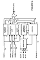
- FIG. 2 is a block diagram of address decoder 10.
- Address decoder 10 includes a plurality of address decoder modules.
- the address decoder modules are represented by an address decoder module 21, an address decoder module 22 and an address decoder module 23. While three address decoder modules are shown by way of example, it is only required for the present invention that at least two address decoder modules are present. Any number greater than two is acceptable.
- Each address decoder module has a unique device select line for each device.
- address decoder module 21 has a device select line 41 for a first device, a device select line 44 for a second device and a device select line 47 for a third device.
- Address decoder module 22 has a device select line 42 for a first device, a device select line 45 for a second device and a device select line 48 for a third device.
- Address decoder module 23 has a device select line 43 for a first device, a device select line 46 for a second device and a device select line 49 for a third device.
- a state control block 20 is used to select only one of the address decoder modules at a time. State control block 20 will assert the reset signals of the address decoder modules that are not selected.
- state control block 20 when address decoder module 21 is not selected, state control block 20 will use a reset line 31 to assert a reset signal to address decoder module 21. When address decoder module 22 is not selected, state control block 20 will use a reset line 32 to assert a reset signal to address decoder module 22. When address decoder module 23 is not selected, state control block 20 will use a reset line 33 to assert a reset signal to address decoder module 23.
- Logic XOR circuitry 24 is used to select an active select signal for the first device to be forwarded to device select line 37. XOR circuitry 24 guarantees that one and only one device select line from device select lines 41, 42 and 43 are asserted before an active select signal for the first device is forwarded to device select line 37. If more than one device select line from device select lines 41, 42 and 43 are asserted at the same time, this indicates that more than one address decoder modules are simultaneously active; therefore, XOR circuitry 24 will not assert select line 37 and a bus error will result.
- Logic XOR circuitry 25 is used to select an active select signal for the first device to be forwarded to device select line 38.
- XOR circuitry 25 guarantees that one and only one device select line from device select lines 44, 45 and 46 are asserted before an active select signal for the first device is forwarded to device select line 38. If more than one device select line from device select lines 44, 45 and 46 are asserted at the same time, this indicates that more than one address decoder modules are simultaneously active; therefore, XOR circuitry 25 will not assert select line 38 and a bus error will result.
- Logic XOR circuitry 26 is used to select an active select signal for the first device to be forwarded to device select line 39. XOR circuitry 26 guarantees that one and only one device select line from device select lines 47, 48 and 49 are asserted before an active select signal for the first device is forwarded to device select line 39. If more than one device select line from device select lines 47, 48 and 49 are asserted at the same time, this indicates that more than one address decoder modules are simultaneously active; therefore, XOR circuitry 26 will not assert select line 39 and a bus error will result.
- State control block 20 detects state changes, for example, by monitoring a value within a register, or by logic detecting a state change within a processor.
- a state change may be from a normal state to a secure state, or from a normal state to a test state.
- FIG 3 shows simplified input/output (I/O) for an address decoder module 50 which is representative of the address decoder modules shown in Figure 2 .
- Address decoder module 50 is designed to work with an AMBA System Bus (ASB).
- ASB AMBA System Bus
- Address decoder module 50 provides centralized address decoding for two or more ASB slave peripherals.
- Address decoder module 50 provides a default transfer response and can be configured for both high and low speed operation.
- Address decoder module 50 can be configured to also serve as a protection unit.
- a scan test mode (ScanTestMode) input pin 51 when asserted high puts address decoder module 50 into the test state.
- the transfer response tristates of address decoder module 50 are disabled and slave select (dsel) output pins 64 will always select one and only one slave.
- a decoder enable (DecEnable) latch within address decoder module 50 is always transparent, and internal test points are enabled.
- Two-bit transfer type (btran[1:0]) input bus pins 52 receive input which indicates the transfer type of the next bus transaction.
- Thirty-two bit address (ba[31:0]) input bus pins 53 receive the AMBA system bus address.
- a transfer direction (bwrite) input pin 54 receives an indication of the transfer direction. When bwrite is low, this indicates a read cycle. When bwrite is high this indicates a write cycle.
- Two-bit transfer size (bsize[1:0] input bus pins 55 indicate the size of the data word to be transmitted.
- Two-bit protection control (bprot[1:0]) input bus pins 56 provides information about the transfer type to implement basic transfer protection. Information includes whether the data is an opcode or data, and whether the access mode is user or supervisor.
- a bus clock (bclk) input pin 57 receives the system bus clock.
- a not bus clock (nbclk) input pin 58 receives the inverted system bus clock.
- a reset (bnres) input pin 59 receives a reset signal which, when low, resets both address decoder module 50.
- a wait response (bwait) bi-directional pin 60 carries a signal which, when high indicates that at least one additional cycle is needed to complete the bus transaction, and when low indicates the transaction should complete in the current cycle.
- An error response (berror) bi-directional pin 61 carries a signal which, when high indicates a transfer error has occurred, and when low indicates the transfer is proceeding correctly. Error response (berror) bi-directional pin 61 is also used with last response (blast) bi-directional pin 62 to indicate a bus retraction.
- a last response (blast) bi-directional pin 62 carries a signal which when high indicates that another cycle is needed for address decoding, and when low indicates that a burst sequence may continue.
- Last response (blast) bi-directional pin 62 is also used with error response (berror) bi-directional pin 61 to indicate a bus retraction.
- Slave select (dsel [y:0]) output bus pins 64 generates signals for a bus consisting of enables for each slave device. Exactly one or none of the slaves is selected at a given time. When a single pin (dsel[x]) of slave select (dsel [y:0]) output bus pins 64 is high, this indicates that slave x is selected. When a single pin (dsel[x]) of slave select (dsel [y:0]) output bus pins 64 is low, this indicates that slave x is not selected.
- Figure 4 is a simplified block diagram of address decoder module 50.
- An address region 72, a memory transfer response block 75, a transceiver 71, a set of logical AND gates 78 and a control block 76 provide address decoding functionality for address decoder module 50.
- the address decoding functionality centrally decodes an address and selects an appropriate slave device.
- the address decode consists simply of an upper order bit tag compare. If the address region is not a power of 2, then identical upper order bits are tag compared. The non-matching lower order bits are then compared, except for address ranges starting with 0 or ending in 0xFFFFFF, using two comparators. For the degenerate region starting at zero, the range 0 to A is determined by just a ⁇ A. Likewise, the region A to 0xFFFFFFFFFF is determined by just a ⁇ A.
- Address region 72 detects an error and asserts, through a logic OR gate 77, an error input 85 to control 76 when a user accesses an address region that contains no slave, an error response is produced.
- a memory boundary check block 74 is included so that while address decoder module 50 is decoding the address, it also determines if a sequential access will still be in the active address region. To do this, memory boundary check block 74 checks the current address against the upper bounds for all address regions. The low order address bit (A[0]) of the address (ba[31:0]) input bus is ignored for word and half-word transfers. The second lowest order address bit (A[1]) of address (ba[31:0]) input bus is ignored for word transfers. If the current address matches one of the upper bounds, then a DecLast signal on a line 84 is asserted and address decoder module 50 inserts a wait state.
- the address decoder module 50 provides additional access protection. This additional protection is provided by a protection unit 73. Protection unit 73 generates an error signal which is forwarded through logic OR gate 77 to error input 85 of control block 76.
- Protection unit 73 detects an access alignment violation if the user accesses a data word at an address with a suffix other than 00, or accesses a halfword at an address with a suffix other than 0. In this case protection unit 73 generates an error signal. Detection of this type of violation can be disabled.
- Protection unit 73 detects a read/write violation when an attempt is made to read from a write only region or to write to a read only region will produce an error response. In this case protection unit 73 generates an error signal.
- Protection unit 73 detects a supervisor region access error when a user accesses a region marked for supervisor access only. In this case protection unit 73 generates an error signal.
- Protection unit 73 detects an incorrect transfer size error if the user accesses an address with an unsupported transfer size (Byte, Halfword, or Word). In this case protection unit 73 generates an error signal.
- Protection unit 73 detects a data type error when opcode fetch to a region marked as data only is attempted or a data access to a region marked as opcode only is attempted. In either case protection unit 73 generates an error signal.
Claims (10)
- Adressdecodierer, umfassend:eine Vielzahl von Adressdecodierermodulen, wobei jedes Adressdecodierermodul aus der Vielzahl von Adressdecodierermodulen eine Auswahlleitung für jede aus einer Vielzahl von Vorrichtungen aufweist;eine Vielzahl von XOR-Kombinationsschaltungen, wobei jede XOR-Kombinationsschaltung aus der Vielzahl von XOR-Kombinationsschaltungen eine logische XOR-Funktion aller Auswahlleitungen für eine einzelne Vorrichtung aus der Vielzahl von Vorrichtungen ausführt; undZustandssteuermittel zum Aktivieren eines Adressdecodierermoduls aus der Vielzahl der Adressdecodierermodule zu einem Zeitpunkt.
- Adressdecodierer nach Anspruch 1, wobei jedes Adressdecodierermodul aus der Vielzahl von Adressdecodierer modulen mit einem Adressbus verbunden ist.
- Adressdecodierer nach Anspruch 1, wobei das Zustandssteuermittel Rücksetzsignale aller Adressdecodierermodule, die nicht aktiviert sind, aus der Vielzahl von Adressdecodierermodulen setzt.
- Adressdecodierer nach Anspruch 1, wobei eine Zugrifferlaubnisebene, die zum Zugreifen auf eine Vorrichtung erforderlich ist, in Abhängigkeit davon variiert, welches Adressdecodierermodul aktiviert ist.
- Adressdecodierer nach Anspruch 1, wobei eine Basisadresse, die zum Zugreifen auf eine Vorrichtung verwendet wird, in Abhängigkeit davon variiert, welches Adressdecodierermodul aktiviert ist.
- Verfahren zum Decodieren von Adressen, das die folgenden Schritte umfasst:(a) Aktivieren eines Adressdecodierermoduls aus einer Vielzahl von Adressdecodierermodulen zu einem Zeitpunkt, wobei jedes Adressdecodierermodul aus der Vielzahl von Adressdecodierermodulen eine Auswahlleitung für jede Vorrichtung in einer Vielzahl von Vorrichtungen aufweist;(b) Aktivieren einer ersten Auswahlleitung für eine erste Vorrichtung aus der Vielzahl von Vorrichtungen durch das Adressdecodierermodul aus der Vielzahl von Adressdecodierermodulen; und(c) für jede Vorrichtung in der Vielzahl der Vorrichtungen, Ausführen einer logischen XOR-Funktion aller Auswahlleitungen für die Vorrichtung.
- Verfahren nach Anspruch 6, wobei im Schritt (a) jedes Adressdecodierermodul aus der Vielzahl von Adressdecodierermodulen mit einem Adressbus verbunden ist.
- Verfahren nach Anspruch 6, wobei der Schritt (a) den folgenden Unterschritt enthält:(a.1) Setzen von Rücksetzsignalen aller Adressdecodierermodule, die nicht aktiviert sind, aus der Vielzahl von Adressdecodierermodulen durch eine Zustandssteuerlogik.
- Verfahren nach Anspruch 6, wobei eine Zugrifferlaubnisebene, die zum Zugreifen auf eine Vorrichtung erforderlich ist, in Abhängigkeit davon variiert, welches Adressdecodierermodul aktiviert ist.
- Verfahren nach Anspruch 6, wobei eine Basisadresse, die zum Zugreifen auf eine Vorrichtung verwendet wird, in Abhängigkeit davon variiert, welches Adressdecodierermodul aktiviert ist.
Applications Claiming Priority (3)
| Application Number | Priority Date | Filing Date | Title |
|---|---|---|---|
| US09/241,263 US6260132B1 (en) | 1999-02-01 | 1999-02-01 | Method and apparatus for secure address re-mapping |
| US241263 | 1999-02-01 | ||
| PCT/US1999/028356 WO2000045272A1 (en) | 1999-02-01 | 1999-11-30 | Method and apparatus for secure address re-mapping |
Publications (2)
| Publication Number | Publication Date |
|---|---|
| EP1066567A1 EP1066567A1 (de) | 2001-01-10 |
| EP1066567B1 true EP1066567B1 (de) | 2009-08-12 |
Family
ID=22909958
Family Applications (1)
| Application Number | Title | Priority Date | Filing Date |
|---|---|---|---|
| EP99962947A Expired - Lifetime EP1066567B1 (de) | 1999-02-01 | 1999-11-30 | Verfahren und einrichtung zur gesicherten adresswiederabbildung |
Country Status (6)
| Country | Link |
|---|---|
| US (1) | US6260132B1 (de) |
| EP (1) | EP1066567B1 (de) |
| JP (1) | JP2002536718A (de) |
| CN (1) | CN1154930C (de) |
| DE (1) | DE69941253D1 (de) |
| WO (1) | WO2000045272A1 (de) |
Families Citing this family (7)
| Publication number | Priority date | Publication date | Assignee | Title |
|---|---|---|---|---|
| JP4014801B2 (ja) * | 2000-12-28 | 2007-11-28 | 株式会社ルネサステクノロジ | 不揮発性メモリ装置 |
| US7773754B2 (en) * | 2002-07-08 | 2010-08-10 | Broadcom Corporation | Key management system and method |
| US7469338B2 (en) * | 2002-07-29 | 2008-12-23 | Broadcom Corporation | System and method for cryptographic control of system configurations |
| US7822797B2 (en) * | 2002-07-29 | 2010-10-26 | Broadcom Corporation | System and method for generating initial vectors |
| KR100947213B1 (ko) * | 2005-04-06 | 2010-03-11 | 브로드콤 코포레이션 | 멀티미디어 프로세서 내의 보안 조건부 액세스 및 디지털권한 관리 기법 |
| US8402188B2 (en) * | 2008-11-10 | 2013-03-19 | Micron Technology, Inc. | Methods and systems for devices with a self-selecting bus decoder |
| CN106933751B (zh) * | 2015-12-29 | 2019-12-24 | 澜起科技股份有限公司 | 用于保护动态随机访问存储器的方法和设备 |
Family Cites Families (9)
| Publication number | Priority date | Publication date | Assignee | Title |
|---|---|---|---|---|
| EP0471928B1 (de) * | 1990-08-20 | 1999-07-14 | Kabushiki Kaisha Toshiba | Verbindungszustandsbestätigungssystem und -methode für eine Expansionseinheit |
| JPH05225798A (ja) * | 1991-08-14 | 1993-09-03 | Internatl Business Mach Corp <Ibm> | メモリシステム |
| US5559992A (en) | 1993-01-11 | 1996-09-24 | Ascom Autelca Ag | Apparatus and method for protecting data in a memory address range |
| JPH07192481A (ja) * | 1993-12-27 | 1995-07-28 | Mitsubishi Electric Corp | 半導体記憶装置 |
| US5706407A (en) | 1993-12-28 | 1998-01-06 | Kabushiki Kaisha Toshiba | System for reallocation of memory banks in memory sized order |
| US5617559A (en) | 1994-08-31 | 1997-04-01 | Motorola Inc. | Modular chip select control circuit and method for performing pipelined memory accesses |
| US5964825A (en) * | 1996-02-09 | 1999-10-12 | Texas Instruments Incorporated | Manipulation of boolean values and conditional operation in a microprocessor |
| US5963104A (en) * | 1996-04-15 | 1999-10-05 | Vlsi Technology, Inc. | Standard cell ring oscillator of a non-deterministic randomizer circuit |
| US5657291A (en) * | 1996-04-30 | 1997-08-12 | Sun Microsystems, Inc. | Multiport register file memory cell configuration for read operation |
-
1999
- 1999-02-01 US US09/241,263 patent/US6260132B1/en not_active Expired - Lifetime
- 1999-11-30 CN CNB998069167A patent/CN1154930C/zh not_active Expired - Fee Related
- 1999-11-30 WO PCT/US1999/028356 patent/WO2000045272A1/en active Application Filing
- 1999-11-30 JP JP2000596462A patent/JP2002536718A/ja not_active Withdrawn
- 1999-11-30 EP EP99962947A patent/EP1066567B1/de not_active Expired - Lifetime
- 1999-11-30 DE DE69941253T patent/DE69941253D1/de not_active Expired - Lifetime
Also Published As
| Publication number | Publication date |
|---|---|
| US6260132B1 (en) | 2001-07-10 |
| EP1066567A1 (de) | 2001-01-10 |
| JP2002536718A (ja) | 2002-10-29 |
| DE69941253D1 (de) | 2009-09-24 |
| CN1304508A (zh) | 2001-07-18 |
| CN1154930C (zh) | 2004-06-23 |
| WO2000045272A1 (en) | 2000-08-03 |
Similar Documents
| Publication | Publication Date | Title |
|---|---|---|
| JP4234202B2 (ja) | コンピュータシステムのi/oアドレス空間にマップされたレジスタへのアクセスを制御するためのシステム | |
| US4959860A (en) | Power-on password functions for computer system | |
| US5450576A (en) | Distributed multi-processor boot system for booting each processor in sequence including watchdog timer for resetting each CPU if it fails to boot | |
| US7149854B2 (en) | External locking mechanism for personal computer memory locations | |
| CA1182927A (en) | Memory management arrangement for microprocessor systems | |
| US7277972B2 (en) | Data processing system with peripheral access protection and method therefor | |
| EP0382470A2 (de) | Rechner mit Tastaturkennwortfunktionen | |
| US5704039A (en) | Mask programmable security system for a data processor and method therefor | |
| WO1994008296A1 (en) | Double buffering operations between the memory bus and the expansion bus of a computer system | |
| JPH07191903A (ja) | データ処理システムおよび動作方法 | |
| GB2070821A (en) | Memory protection | |
| US6546482B1 (en) | Invalid configuration detection resource | |
| JP2006091972A (ja) | バスシステム及び半導体集積回路 | |
| US6678838B1 (en) | Method to track master contribution information in a write buffer | |
| EP1066567B1 (de) | Verfahren und einrichtung zur gesicherten adresswiederabbildung | |
| WO2008030727A2 (en) | Access control of memory space in microprocessor systems | |
| JP3995883B2 (ja) | マルチタスク・システムのためのメモリ保護システム | |
| KR100252254B1 (ko) | 이기종 메모리 모듈의 혼용이 가능한 컴퓨터 시스템 | |
| JPS6329859A (ja) | 記憶保護装置 | |
| CN116662984A (zh) | 内存隔离装置以及基于内存隔离装置的多核计算系统 | |
| GB2385956A (en) | key based register locking system | |
| CN116361233A (zh) | 一种微控制器 | |
| KR960702651A (ko) | 보안성 메모리 카드 | |
| JP2777236B2 (ja) | コンピュータシステムおよびコンピュータシステムの構成変更方法 | |
| JPH01258054A (ja) | 記憶装置のアクセス制御方式 |
Legal Events
| Date | Code | Title | Description |
|---|---|---|---|
| PUAI | Public reference made under article 153(3) epc to a published international application that has entered the european phase |
Free format text: ORIGINAL CODE: 0009012 |
|
| AK | Designated contracting states |
Kind code of ref document: A1 Designated state(s): AT BE CH CY DE DK ES FI FR GB GR IE IT LI LU MC NL PT SE |
|
| 17P | Request for examination filed |
Effective date: 20010205 |
|
| RBV | Designated contracting states (corrected) |
Designated state(s): DE FR GB |
|
| RAP1 | Party data changed (applicant data changed or rights of an application transferred) |
Owner name: NXP B.V. |
|
| GRAP | Despatch of communication of intention to grant a patent |
Free format text: ORIGINAL CODE: EPIDOSNIGR1 |
|
| GRAS | Grant fee paid |
Free format text: ORIGINAL CODE: EPIDOSNIGR3 |
|
| GRAA | (expected) grant |
Free format text: ORIGINAL CODE: 0009210 |
|
| AK | Designated contracting states |
Kind code of ref document: B1 Designated state(s): DE FR GB |
|
| REG | Reference to a national code |
Ref country code: GB Ref legal event code: FG4D |
|
| REF | Corresponds to: |
Ref document number: 69941253 Country of ref document: DE Date of ref document: 20090924 Kind code of ref document: P |
|
| PLBE | No opposition filed within time limit |
Free format text: ORIGINAL CODE: 0009261 |
|
| STAA | Information on the status of an ep patent application or granted ep patent |
Free format text: STATUS: NO OPPOSITION FILED WITHIN TIME LIMIT |
|
| 26N | No opposition filed |
Effective date: 20100517 |
|
| PGFP | Annual fee paid to national office [announced via postgrant information from national office to epo] |
Ref country code: DE Payment date: 20121025 Year of fee payment: 14 |
|
| PGFP | Annual fee paid to national office [announced via postgrant information from national office to epo] |
Ref country code: GB Payment date: 20121025 Year of fee payment: 14 |
|
| PGFP | Annual fee paid to national office [announced via postgrant information from national office to epo] |
Ref country code: FR Payment date: 20130107 Year of fee payment: 14 |
|
| GBPC | Gb: european patent ceased through non-payment of renewal fee |
Effective date: 20131130 |
|
| REG | Reference to a national code |
Ref country code: FR Ref legal event code: ST Effective date: 20140731 |
|
| REG | Reference to a national code |
Ref country code: DE Ref legal event code: R119 Ref document number: 69941253 Country of ref document: DE Effective date: 20140603 |
|
| PG25 | Lapsed in a contracting state [announced via postgrant information from national office to epo] |
Ref country code: DE Free format text: LAPSE BECAUSE OF NON-PAYMENT OF DUE FEES Effective date: 20140603 |
|
| PG25 | Lapsed in a contracting state [announced via postgrant information from national office to epo] |
Ref country code: GB Free format text: LAPSE BECAUSE OF NON-PAYMENT OF DUE FEES Effective date: 20131130 Ref country code: FR Free format text: LAPSE BECAUSE OF NON-PAYMENT OF DUE FEES Effective date: 20131202 |