EP1064673B1 - Slip free vertical rack design having rounded horizontal arms - Google Patents
Slip free vertical rack design having rounded horizontal arms Download PDFInfo
- Publication number
- EP1064673B1 EP1064673B1 EP99936141A EP99936141A EP1064673B1 EP 1064673 B1 EP1064673 B1 EP 1064673B1 EP 99936141 A EP99936141 A EP 99936141A EP 99936141 A EP99936141 A EP 99936141A EP 1064673 B1 EP1064673 B1 EP 1064673B1
- Authority
- EP
- European Patent Office
- Prior art keywords
- vertical
- horizontal
- support means
- wafer
- surface portion
- Prior art date
- Legal status (The legal status is an assumption and is not a legal conclusion. Google has not performed a legal analysis and makes no representation as to the accuracy of the status listed.)
- Expired - Lifetime
Links
Images


Classifications
-
- H—ELECTRICITY
- H10—SEMICONDUCTOR DEVICES; ELECTRIC SOLID-STATE DEVICES NOT OTHERWISE PROVIDED FOR
- H10P—GENERIC PROCESSES OR APPARATUS FOR THE MANUFACTURE OR TREATMENT OF DEVICES COVERED BY CLASS H10
- H10P95/00—Generic processes or apparatus for manufacture or treatments not covered by the other groups of this subclass
-
- H—ELECTRICITY
- H10—SEMICONDUCTOR DEVICES; ELECTRIC SOLID-STATE DEVICES NOT OTHERWISE PROVIDED FOR
- H10P—GENERIC PROCESSES OR APPARATUS FOR THE MANUFACTURE OR TREATMENT OF DEVICES COVERED BY CLASS H10
- H10P72/00—Handling or holding of wafers, substrates or devices during manufacture or treatment thereof
- H10P72/10—Handling or holding of wafers, substrates or devices during manufacture or treatment thereof using carriers specially adapted therefor, e.g. front opening unified pods [FOUP]
- H10P72/12—Vertical boat type carrier whereby the substrates are horizontally supported, e.g. comprising rod-shaped elements
- H10P72/127—Vertical boat type carrier whereby the substrates are horizontally supported, e.g. comprising rod-shaped elements characterised by the substrate support
-
- H—ELECTRICITY
- H10—SEMICONDUCTOR DEVICES; ELECTRIC SOLID-STATE DEVICES NOT OTHERWISE PROVIDED FOR
- H10P—GENERIC PROCESSES OR APPARATUS FOR THE MANUFACTURE OR TREATMENT OF DEVICES COVERED BY CLASS H10
- H10P72/00—Handling or holding of wafers, substrates or devices during manufacture or treatment thereof
- H10P72/10—Handling or holding of wafers, substrates or devices during manufacture or treatment thereof using carriers specially adapted therefor, e.g. front opening unified pods [FOUP]
- H10P72/12—Vertical boat type carrier whereby the substrates are horizontally supported, e.g. comprising rod-shaped elements
- H10P72/123—Vertical boat type carrier whereby the substrates are horizontally supported, e.g. comprising rod-shaped elements characterised by a material, a roughness, a coating or the like
Definitions
- the semiconductor manufacturing industry typically processes these wafers in either horizontal or vertical carriers.
- the horizontal carrier typically called a “boat” has three or four horizontally disposed bars arranged in a semicircle design, with each bar having inwardly facing grooves set therein at regular intervals. Each set of grooves define a vertical space for carrying a vertically disposed wafer.
- the vertical carrier typically called a “vertical rack” has three or four vertically disposed rods (or posts) arranged in a semicircle design, with each post having slots set therein at regular intervals to define a space for supporting a horizontally disposed wafer. To insure the geometrical precision required in this field, the three or four rods are fixed to a top plate and a bottom plate. The portions of the post between each slot, termed “teeth”, are identically spaced in order to support wafers at regular intervals from and parallel to the bottom plate. The entire rack is then placed within a vertical furnace for processing the wafers.
- the rack which produces “near center support” has eliminated slip in many wafer processing applications, it is somewhat inefficient, as the portion of its arm which rises from the horizontal plane to produce the near-center support necessarily increases the vertical spacing period of the rack, that is, the wafer-to-wafer distance. Tanaka, for example, specifically teaches that its riser vertically extend at least about 0.3 mm from the flat portion of the tooth. Accordingly, the near-center support style of vertical rack can typically accommodate only about 90% of the wafers typically accommodated by the conventional vertical rack.
- Figure 3(b) of Tomanovich discloses a vertical rack wherein the arms are strictly horizontal and do not rise. Although this rack has been found to eliminate slip in some high temperature semiconductor wafer processing applications, it performs less well in more demanding applications.
- EP 0807961 A1 discloses a vertical rack in which the horizontal arms have rounded edges.
- Nakajima there is no recognition in Nakajima of the need to make the surface roughness of the horizontal portion as low as 1 um in order to prevent slip under extreme conditions.
- Example 1 of Nakajima teaches that a surface roughness of 5-58 um is perfectly fine
- Nakajima teaches away from providing a rack wherein the horizontal arms have a surface roughness of no more than 1 um.
- the rack of the present invention comprises an arm which first extends strictly horizontally from the vertical rod and then slopes gently downward, and has a smooth upper surface. Preliminary experiments involving the rack of the present invention have shown that it has essentially eliminated slip in 200 mm silicon wafers in a 1200°C wafer processing application. By contrast, a similarly dimensioned vertical rack having strictly horizontal arms (i.e., Figure 3b of Tomanovich) produced slip in about 50% of the wafers in the same processing application.
- the rack of the present invention is more compact and efficient than the near-center support racks (as it has no riser) and is more effective at preventing slip than the strictly horizontal arm rack.
- this rack is surprising in that its design would appear to encourage slip but in fact prevents slip. Specifically, the near center support racks seek to prevent slip by preventing too much sag in the inner portions of the wafer. By providing a gently downsloping edge (or "rounded") portion, the rack of the present invention appears to promote sag in the inner portions of the wafer. However, this design has demonstrated effectiveness in preventing slip.
- the design of the present invention takes advantage of the monocrystalline nature of the silicon wafer.
- the silicon wafer responds elastically in semiconductor wafer processing by slightly sagging as it is exposed to high temperatures and then regaining its initial flatness as it cools. It appears that only when the sagging wafer is also confronted with a region of stress concentration (i.e., its sag is interrupted by a sharp supporting edge) does it produce slip. Because the edge of the support arm of the present invention is rounded, the slightly sagging wafer is supported about an increased surface area whose pitch essentially eliminates (or substantially reduces) stress concentration. It is believed that both the increased surface area (which provides more support to the sagging wafer) and the rounded nature of the edge (which prevents stress concentration) each have a role in the successful application of this rack.
- the vertical portion of the vertical rack further comprises an arcuate horizontal cross-section defining a maximum radius R max having a centerpoint, the plurality of vertically spaced, horizontal support means horizontally extend from the vertical portion substantially towards the centerpoint, the horizontal upper surface portion extends continuously horizontally from the vertical portion towards the centerpoint for a distance of at least 20% of R max , and the rounded upper surface portion slopes downward from the horizontal upper surface portion towards the centerpoint.
- a preferred vertical rack 11/ wafer W combination comprising:
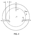
- Figure 2 shows how the rods 14 are oriented to form a horizontal cross-section defining a maximum radius R max (as shown by the dotted line) having a centerpoint C.
- R max as shown by the dotted line
- the dotted line would also correspond to the largest wafer which could be accommodated by the rack.
- the innermost contact between at least one and preferably each of at least three of the arms and their supported wafer is in the region of between 33% and 66% of the wafer radius.
- the total contact area between the arms of one support level and their supported wafer is typically between about 1% and about 5% of the surface area of the wafer face which contacts the arms.
- the surfaces of the arms upon which the wafers are supported i.e., both the horizontal portion of the arm and its downsloping edge
- a surface roughness Ra of no more than 1 um, as defined by Section 3.9.1 of ANSI/ASME National Standard B46.1-1985. If the smoothness of the horizontal portion is about 2 um, then when the wafer expands during heat up, the peak portions of the arms will prevent the smooth expansion of the wafer and this phenomenon will cause slip.
- the rack of the present invention is more advantageously used when processing wafers having a diameter of at least 200 mm (about 8 inch), more advantageously with wafers having a diameter of at least 250 mm (about 10 inch), and most advantageously with wafers having a diameter of at least 300 mm (about 12 inch).
- vertical racks of the present invention whose vertical rods define a wafer supporting diameter of at least 200 mm provide special advantage. More advantage is provided when the vertical rods define a wafer supporting diameter of at least 250 mm, and even greater advantage is provided when the vertical rods define a wafer supporting diameter of at least 300 mm.
- the rack of the present invention is more advantageously used when the temperature of the wafer becomes at least about 1000°C for at least 15 minutes. More advantage is provided when the temperature of the wafer becomes at least about 1100°C and even greater advantage is provided when the temperature of the wafer becomes at least about 1200°C for at least 30 minutes.
- the angle of deviation of the horizontal upper surface portion of the arm from horizontal is typically between about 0° and 0.2° degrees.
- the rounded edge of the arm not only provides an increased support area for the wafer during its critical sagging state, but also is free of stress concentrating features.
- the curvature of the rounded edge is preferably substantially hemispherical and defines a radius R of between 3 mm and 50 mm, more preferably between 5 mm and 20 mm. Its surface roughness Ra is generally no more than about 2 um, preferably no more than 1 um.
- the rounded edge provides a downward sloping support face having a grade of about 1/10 (i.e., it slopes downward about 0.5 mm over the last 5 mm of the arm). Generally, the rounded edge provides a downward sloping support face having a grade of between about 1/30 and 1/3.
- the lateral edges 21 of the arms are rounded.
- the distance which the horizontal upper surface portion typically extends from its vertical rod is generally dependent upon the size of the wafer to be processed. For example, when the wafer to be processed has a 6 inch diameter, the horizontal upper surface portion typically terminates at least 15 mm from the edge of the rod, usually between about 20 mm and about 40 mm from the rod, and preferably about 27 mm from the edge of the rod. When the wafer to be processed has an 8 inch diameter, the horizontal upper surface portion typically terminates at least 22 mm from the edge of the rod, usually between about 30 mm and about 50 mm from the rod, and preferably about 36 mm from the edge of the rod. When the wafer to be processed has an 12 inch diameter, the horizontal upper surface portion typically terminates at least 30 mm from the edge of the rod, usually between about 40 mm and about 70 mm from the rod, and preferably about 54 mm from the edge of the rod.
- the horizontal upper surface portion of the arm supports the wafer from its periphery to a distance corresponding to between 20% and 80% of the supported wafer radius, more typically between 33% and 66% of the wafer radius.
- the vertical rack of the present invention can be made from any ceramic material having an iron purity which allows its use in the high temperature production of vertical racks for semiconductor processing.
- the material is recrystallized silicon carbide. More preferably, the recrystallized silicon carbide component has less than 10 ppm iron.
- the rack material may also be CVD coated with refractory materials such as silicon carbide, silicon nitride or diamond.
- the rack comprises CRYSTAR, a recrystallized silicon carbide available from the Norton Company of Worcester, MA.
- the rack material comprises siliconized silicon carbide.
- the rack material has a 1200°C flexural strength (4 point) of at least 150 MPa.
- the arms of vertical racks typically shield, or "shadow", radiant heat and/or reactive gases (which enter from the periphery of the vertical furnace) from the portions of the wafer inside of and adjacent to the posts. Accordingly, significant variations in temperature and/or gas concentration between the "shadowed" portion of the wafer and the rest of the wafer are produced. These variations contribute to slip-inducing stress. Therefore, in some embodiments, the arms are radially oriented such that they cast a shadow on no more than 30% of the wafer, preferably no more than 10% of the wafer.
- the shadow percentage is calculated by determining the percentage of the wafer face to which reactant gases and/or heat can directly radially proceed from the rack periphery in a path unobstructed by the arms.
- the shaded portion of Figure 3 represents the shadow produced by the rods of Figure 2 upon the wafer.
Landscapes
- Container, Conveyance, Adherence, Positioning, Of Wafer (AREA)
Applications Claiming Priority (3)
| Application Number | Priority Date | Filing Date | Title |
|---|---|---|---|
| US09/031,887 US5931666A (en) | 1998-02-27 | 1998-02-27 | Slip free vertical rack design having rounded horizontal arms |
| US31887 | 1998-02-27 | ||
| PCT/US1999/003625 WO1999044222A1 (en) | 1998-02-27 | 1999-02-19 | Slip free vertical rack design having rounded horizontal arms |
Publications (2)
| Publication Number | Publication Date |
|---|---|
| EP1064673A1 EP1064673A1 (en) | 2001-01-03 |
| EP1064673B1 true EP1064673B1 (en) | 2008-10-01 |
Family
ID=21861930
Family Applications (1)
| Application Number | Title | Priority Date | Filing Date |
|---|---|---|---|
| EP99936141A Expired - Lifetime EP1064673B1 (en) | 1998-02-27 | 1999-02-19 | Slip free vertical rack design having rounded horizontal arms |
Country Status (9)
| Country | Link |
|---|---|
| US (1) | US5931666A (https=) |
| EP (1) | EP1064673B1 (https=) |
| JP (1) | JP2002505518A (https=) |
| KR (1) | KR100404032B1 (https=) |
| CN (1) | CN1126149C (https=) |
| AU (1) | AU3303199A (https=) |
| CA (1) | CA2318968C (https=) |
| DE (1) | DE69939648D1 (https=) |
| WO (1) | WO1999044222A1 (https=) |
Families Citing this family (33)
| Publication number | Priority date | Publication date | Assignee | Title |
|---|---|---|---|---|
| KR20000002833A (ko) * | 1998-06-23 | 2000-01-15 | 윤종용 | 반도체 웨이퍼 보트 |
| US6171400B1 (en) | 1998-10-02 | 2001-01-09 | Union Oil Company Of California | Vertical semiconductor wafer carrier |
| US6225594B1 (en) | 1999-04-15 | 2001-05-01 | Integrated Materials, Inc. | Method and apparatus for securing components of wafer processing fixtures |
| US6205993B1 (en) | 1999-04-15 | 2001-03-27 | Integrated Materials, Inc. | Method and apparatus for fabricating elongate crystalline members |
| US6196211B1 (en) | 1999-04-15 | 2001-03-06 | Integrated Materials, Inc. | Support members for wafer processing fixtures |
| US7055702B1 (en) * | 2000-06-06 | 2006-06-06 | Saint-Gobain Ceramics & Plastics, Inc. | Slip resistant horizontal semiconductor wafer boat |
| ATE506693T1 (de) | 2000-06-30 | 2011-05-15 | Integrated Materials Inc | Silizium-befestigungen für scheibenhaltervorrichtung zur wärmebehandlung und herstellungsverfahren |
| US6455395B1 (en) | 2000-06-30 | 2002-09-24 | Integrated Materials, Inc. | Method of fabricating silicon structures including fixtures for supporting wafers |
| US6450346B1 (en) | 2000-06-30 | 2002-09-17 | Integrated Materials, Inc. | Silicon fixtures for supporting wafers during thermal processing |
| US20020130061A1 (en) * | 2000-11-02 | 2002-09-19 | Hengst Richard R. | Apparatus and method of making a slip free wafer boat |
| US6727191B2 (en) * | 2001-02-26 | 2004-04-27 | Integrated Materials, Inc. | High temperature hydrogen anneal of silicon wafers supported on a silicon fixture |
| JP3931578B2 (ja) * | 2001-03-30 | 2007-06-20 | 信越半導体株式会社 | 気相成長装置 |
| US6629994B2 (en) * | 2001-06-11 | 2003-10-07 | Advanced Cardiovascular Systems, Inc. | Intravascular stent |
| US6835039B2 (en) * | 2002-03-15 | 2004-12-28 | Asm International N.V. | Method and apparatus for batch processing of wafers in a furnace |
| US6582221B1 (en) | 2002-07-19 | 2003-06-24 | Asm International N.V. | Wafer boat and method for treatment of substrates |
| US7256375B2 (en) * | 2002-08-30 | 2007-08-14 | Asm International N.V. | Susceptor plate for high temperature heat treatment |
| US6939132B2 (en) * | 2002-09-30 | 2005-09-06 | Samsung Austin Semiconductor, L.P. | Semiconductor workpiece apparatus |
| US7033126B2 (en) * | 2003-04-02 | 2006-04-25 | Asm International N.V. | Method and apparatus for loading a batch of wafers into a wafer boat |
| US7749196B2 (en) * | 2003-07-02 | 2010-07-06 | Cook Incorporated | Small gauge needle catheterization apparatus |
| US7181132B2 (en) | 2003-08-20 | 2007-02-20 | Asm International N.V. | Method and system for loading substrate supports into a substrate holder |
| US20050205502A1 (en) * | 2004-03-18 | 2005-09-22 | Brown Steven A | Rails for semiconductor wafer carriers |
| US7520566B2 (en) * | 2004-05-26 | 2009-04-21 | Braun Seating Incorporated | Stowable vehicle seat apparatus and method |
| US20060060145A1 (en) * | 2004-09-17 | 2006-03-23 | Van Den Berg Jannes R | Susceptor with surface roughness for high temperature substrate processing |
| US20060065634A1 (en) * | 2004-09-17 | 2006-03-30 | Van Den Berg Jannes R | Low temperature susceptor cleaning |
| US20060150906A1 (en) * | 2005-01-07 | 2006-07-13 | Selen Louis J M | Wafer boat for reduced shadow marks |
| US7972703B2 (en) * | 2005-03-03 | 2011-07-05 | Ferrotec (Usa) Corporation | Baffle wafers and randomly oriented polycrystalline silicon used therefor |
| JP5184040B2 (ja) * | 2007-10-12 | 2013-04-17 | コバレントマテリアル株式会社 | 縦型ウエハボート |
| US20110259840A1 (en) * | 2010-04-23 | 2011-10-27 | Advanced Semiconductor Engineering, Inc. | Semiconductor package magazine |
| FI122720B (fi) | 2010-07-13 | 2012-06-15 | Tamturbo Oy | Turbokompressorin säätöratkaisu |
| US9153466B2 (en) * | 2012-04-26 | 2015-10-06 | Asm Ip Holding B.V. | Wafer boat |
| JP6770461B2 (ja) * | 2017-02-21 | 2020-10-14 | クアーズテック株式会社 | 縦型ウエハボート |
| KR102768950B1 (ko) * | 2020-02-06 | 2025-02-19 | 삼성디스플레이 주식회사 | 기판용 카세트 |
| KR102709165B1 (ko) * | 2021-10-29 | 2024-09-24 | 솔믹스 주식회사 | 웨이퍼 보트 |
Family Cites Families (19)
| Publication number | Priority date | Publication date | Assignee | Title |
|---|---|---|---|---|
| US3660886A (en) * | 1969-02-20 | 1972-05-09 | Ginori Ceramica Ital Spa | Method of making firing setters for tiles and other ceramic articles |
| JPS6216516A (ja) * | 1985-07-15 | 1987-01-24 | Mitsubishi Electric Corp | 半導体製造装置 |
| US5169453A (en) * | 1989-03-20 | 1992-12-08 | Toyoko Kagaku Co., Ltd. | Wafer supporting jig and a decompressed gas phase growth method using such a jig |
| GB9021873D0 (en) * | 1990-10-09 | 1990-11-21 | Groom Bryan Ltd | Ware support apparatus |
| JP3204699B2 (ja) * | 1990-11-30 | 2001-09-04 | 株式会社東芝 | 熱処理装置 |
| JPH05102056A (ja) * | 1991-10-11 | 1993-04-23 | Rohm Co Ltd | ウエハー支持具 |
| JP3234617B2 (ja) * | 1991-12-16 | 2001-12-04 | 東京エレクトロン株式会社 | 熱処理装置用基板支持具 |
| JPH06163440A (ja) * | 1992-11-16 | 1994-06-10 | Shin Etsu Chem Co Ltd | 半導体縦型拡散炉用治具 |
| US5492229A (en) * | 1992-11-27 | 1996-02-20 | Toshiba Ceramics Co., Ltd. | Vertical boat and a method for making the same |
| JP3245246B2 (ja) * | 1993-01-27 | 2002-01-07 | 東京エレクトロン株式会社 | 熱処理装置 |
| JPH07147258A (ja) * | 1993-11-25 | 1995-06-06 | Hitachi Ltd | 半導体ウェハの熱処理装置 |
| JP3316068B2 (ja) * | 1993-12-01 | 2002-08-19 | 東京エレクトロン株式会社 | 熱処理用ボート |
| JPH10510680A (ja) * | 1995-05-05 | 1998-10-13 | サン−ゴバン インダストリアル セラミックス,インコーポレイティド | 滑りのない垂直架台構造 |
| US5534074A (en) * | 1995-05-17 | 1996-07-09 | Heraeus Amersil, Inc. | Vertical boat for holding semiconductor wafers |
| US5706946A (en) * | 1995-06-26 | 1998-01-13 | Kakizaki Manufacturing Co., Ltd | Thin-plate supporting container |
| JPH09251961A (ja) * | 1996-03-15 | 1997-09-22 | Toshiba Corp | 熱処理用ボート |
| JPH09260296A (ja) * | 1996-03-21 | 1997-10-03 | Sumitomo Sitix Corp | ウェーハ支持装置 |
| JPH09306980A (ja) * | 1996-05-17 | 1997-11-28 | Asahi Glass Co Ltd | 縦型ウエハボート |
| JPH10321543A (ja) * | 1997-05-20 | 1998-12-04 | Sumitomo Metal Ind Ltd | ウェハ支持体及び縦型ボート |
-
1998
- 1998-02-27 US US09/031,887 patent/US5931666A/en not_active Expired - Lifetime
-
1999
- 1999-02-19 AU AU33031/99A patent/AU3303199A/en not_active Abandoned
- 1999-02-19 EP EP99936141A patent/EP1064673B1/en not_active Expired - Lifetime
- 1999-02-19 CA CA002318968A patent/CA2318968C/en not_active Expired - Lifetime
- 1999-02-19 CN CN99803417A patent/CN1126149C/zh not_active Expired - Lifetime
- 1999-02-19 DE DE69939648T patent/DE69939648D1/de not_active Expired - Lifetime
- 1999-02-19 JP JP2000533890A patent/JP2002505518A/ja active Pending
- 1999-02-19 KR KR10-2000-7009357A patent/KR100404032B1/ko not_active Expired - Lifetime
- 1999-02-19 WO PCT/US1999/003625 patent/WO1999044222A1/en not_active Ceased
Also Published As
| Publication number | Publication date |
|---|---|
| AU3303199A (en) | 1999-09-15 |
| EP1064673A1 (en) | 2001-01-03 |
| WO1999044222A1 (en) | 1999-09-02 |
| JP2002505518A (ja) | 2002-02-19 |
| CA2318968C (en) | 2004-07-20 |
| KR100404032B1 (ko) | 2003-11-01 |
| KR20010041263A (ko) | 2001-05-15 |
| DE69939648D1 (de) | 2008-11-13 |
| CA2318968A1 (en) | 1999-09-02 |
| US5931666A (en) | 1999-08-03 |
| CN1126149C (zh) | 2003-10-29 |
| CN1292148A (zh) | 2001-04-18 |
Similar Documents
| Publication | Publication Date | Title |
|---|---|---|
| EP1064673B1 (en) | Slip free vertical rack design having rounded horizontal arms | |
| US5865321A (en) | Slip free vertical rack design | |
| US6357604B1 (en) | Long tooth rails for semiconductor wafer carriers | |
| EP1405018B1 (en) | Wafer boat with arcuate wafer support arms | |
| KR100816180B1 (ko) | 반도체 기판용 열처리 치구 및 반도체 기판의 열처리 방법 | |
| US6709267B1 (en) | Substrate holder with deep annular groove to prevent edge heat loss | |
| WO2001004934A1 (en) | Semiconductor wafer carrier | |
| US20010001953A1 (en) | Support apparatus for semiconductor wafer processing | |
| JP2004134761A (ja) | 高温熱処理用のサセプタプレート | |
| US20080041798A1 (en) | Wafer Platform | |
| JP6469046B2 (ja) | 縦型ウエハボート | |
| JP4637475B2 (ja) | 取外し可能なサセプタを用いた半導体基板搬送システム、及び半導体基板の搬送方法 | |
| US8323411B2 (en) | Semiconductor workpiece apparatus | |
| JP4003906B2 (ja) | シリコン単結晶半導体ウエハ加熱処理用治具及びこれを用いたシリコン単結晶半導体ウエハ加熱処理用装置 | |
| JP3831337B2 (ja) | 耐すべり性半導体用水平方向ウェハー用舟形容器 | |
| JP2007529909A (ja) | 半導体ウェーハキャリヤ用改良型レール | |
| JPH1050626A (ja) | 縦型ウエハ支持装置 | |
| MXPA00008370A (en) | Slip free vertical rack design having rounded horizontal arms | |
| JP3867509B2 (ja) | 横型熱処理炉用ボートおよび熱処理方法 | |
| JP2620765B2 (ja) | 縦型拡散炉用ボート | |
| JP2001313267A (ja) | 熱処理用ボート |
Legal Events
| Date | Code | Title | Description |
|---|---|---|---|
| PUAI | Public reference made under article 153(3) epc to a published international application that has entered the european phase |
Free format text: ORIGINAL CODE: 0009012 |
|
| 17P | Request for examination filed |
Effective date: 20000727 |
|
| AK | Designated contracting states |
Kind code of ref document: A1 Designated state(s): DE ES FR GB IT NL SE |
|
| GRAP | Despatch of communication of intention to grant a patent |
Free format text: ORIGINAL CODE: EPIDOSNIGR1 |
|
| GRAS | Grant fee paid |
Free format text: ORIGINAL CODE: EPIDOSNIGR3 |
|
| GRAA | (expected) grant |
Free format text: ORIGINAL CODE: 0009210 |
|
| AK | Designated contracting states |
Kind code of ref document: B1 Designated state(s): DE ES FR GB IT NL SE |
|
| REG | Reference to a national code |
Ref country code: GB Ref legal event code: FG4D |
|
| REF | Corresponds to: |
Ref document number: 69939648 Country of ref document: DE Date of ref document: 20081113 Kind code of ref document: P |
|
| PG25 | Lapsed in a contracting state [announced via postgrant information from national office to epo] |
Ref country code: ES Free format text: LAPSE BECAUSE OF FAILURE TO SUBMIT A TRANSLATION OF THE DESCRIPTION OR TO PAY THE FEE WITHIN THE PRESCRIBED TIME-LIMIT Effective date: 20090112 |
|
| PLBE | No opposition filed within time limit |
Free format text: ORIGINAL CODE: 0009261 |
|
| STAA | Information on the status of an ep patent application or granted ep patent |
Free format text: STATUS: NO OPPOSITION FILED WITHIN TIME LIMIT |
|
| PG25 | Lapsed in a contracting state [announced via postgrant information from national office to epo] |
Ref country code: SE Free format text: LAPSE BECAUSE OF FAILURE TO SUBMIT A TRANSLATION OF THE DESCRIPTION OR TO PAY THE FEE WITHIN THE PRESCRIBED TIME-LIMIT Effective date: 20090101 |
|
| 26N | No opposition filed |
Effective date: 20090702 |
|
| PGFP | Annual fee paid to national office [announced via postgrant information from national office to epo] |
Ref country code: GB Payment date: 20130213 Year of fee payment: 15 |
|
| GBPC | Gb: european patent ceased through non-payment of renewal fee |
Effective date: 20140219 |
|
| PG25 | Lapsed in a contracting state [announced via postgrant information from national office to epo] |
Ref country code: GB Free format text: LAPSE BECAUSE OF NON-PAYMENT OF DUE FEES Effective date: 20140219 |
|
| REG | Reference to a national code |
Ref country code: FR Ref legal event code: PLFP Year of fee payment: 18 |
|
| REG | Reference to a national code |
Ref country code: FR Ref legal event code: PLFP Year of fee payment: 19 |
|
| REG | Reference to a national code |
Ref country code: FR Ref legal event code: PLFP Year of fee payment: 20 |
|
| PGFP | Annual fee paid to national office [announced via postgrant information from national office to epo] |
Ref country code: NL Payment date: 20180214 Year of fee payment: 20 |
|
| PGFP | Annual fee paid to national office [announced via postgrant information from national office to epo] |
Ref country code: DE Payment date: 20180206 Year of fee payment: 20 |
|
| PGFP | Annual fee paid to national office [announced via postgrant information from national office to epo] |
Ref country code: FR Payment date: 20180111 Year of fee payment: 20 Ref country code: IT Payment date: 20180221 Year of fee payment: 20 |
|
| REG | Reference to a national code |
Ref country code: DE Ref legal event code: R071 Ref document number: 69939648 Country of ref document: DE |
|
| REG | Reference to a national code |
Ref country code: NL Ref legal event code: MK Effective date: 20190218 |