EP1061557A2 - Substrate processing apparatus - Google Patents
Substrate processing apparatus Download PDFInfo
- Publication number
- EP1061557A2 EP1061557A2 EP00112620A EP00112620A EP1061557A2 EP 1061557 A2 EP1061557 A2 EP 1061557A2 EP 00112620 A EP00112620 A EP 00112620A EP 00112620 A EP00112620 A EP 00112620A EP 1061557 A2 EP1061557 A2 EP 1061557A2
- Authority
- EP
- European Patent Office
- Prior art keywords
- substrate
- processing
- holder
- chamber
- magnetic
- Prior art date
- Legal status (The legal status is an assumption and is not a legal conclusion. Google has not performed a legal analysis and makes no representation as to the accuracy of the status listed.)
- Granted
Links
Images



Classifications
-
- H—ELECTRICITY
- H10—SEMICONDUCTOR DEVICES; ELECTRIC SOLID-STATE DEVICES NOT OTHERWISE PROVIDED FOR
- H10P—GENERIC PROCESSES OR APPARATUS FOR THE MANUFACTURE OR TREATMENT OF DEVICES COVERED BY CLASS H10
- H10P95/00—Generic processes or apparatus for manufacture or treatments not covered by the other groups of this subclass
-
- H—ELECTRICITY
- H10—SEMICONDUCTOR DEVICES; ELECTRIC SOLID-STATE DEVICES NOT OTHERWISE PROVIDED FOR
- H10P—GENERIC PROCESSES OR APPARATUS FOR THE MANUFACTURE OR TREATMENT OF DEVICES COVERED BY CLASS H10
- H10P72/00—Handling or holding of wafers, substrates or devices during manufacture or treatment thereof
- H10P72/04—Apparatus for manufacture or treatment
- H10P72/0402—Apparatus for fluid treatment
- H10P72/0418—Apparatus for fluid treatment for etching
-
- C—CHEMISTRY; METALLURGY
- C23—COATING METALLIC MATERIAL; COATING MATERIAL WITH METALLIC MATERIAL; CHEMICAL SURFACE TREATMENT; DIFFUSION TREATMENT OF METALLIC MATERIAL; COATING BY VACUUM EVAPORATION, BY SPUTTERING, BY ION IMPLANTATION OR BY CHEMICAL VAPOUR DEPOSITION, IN GENERAL; INHIBITING CORROSION OF METALLIC MATERIAL OR INCRUSTATION IN GENERAL
- C23C—COATING METALLIC MATERIAL; COATING MATERIAL WITH METALLIC MATERIAL; SURFACE TREATMENT OF METALLIC MATERIAL BY DIFFUSION INTO THE SURFACE, BY CHEMICAL CONVERSION OR SUBSTITUTION; COATING BY VACUUM EVAPORATION, BY SPUTTERING, BY ION IMPLANTATION OR BY CHEMICAL VAPOUR DEPOSITION, IN GENERAL
- C23C16/00—Chemical coating by decomposition of gaseous compounds, without leaving reaction products of surface material in the coating, i.e. chemical vapour deposition [CVD] processes
- C23C16/44—Chemical coating by decomposition of gaseous compounds, without leaving reaction products of surface material in the coating, i.e. chemical vapour deposition [CVD] processes characterised by the method of coating
- C23C16/458—Chemical coating by decomposition of gaseous compounds, without leaving reaction products of surface material in the coating, i.e. chemical vapour deposition [CVD] processes characterised by the method of coating characterised by the method used for supporting substrates in the reaction chamber
- C23C16/4582—Rigid and flat substrates, e.g. plates or discs
- C23C16/4583—Rigid and flat substrates, e.g. plates or discs the substrate being supported substantially horizontally
- C23C16/4584—Rigid and flat substrates, e.g. plates or discs the substrate being supported substantially horizontally the substrate being rotated
Definitions
- the present invention relates to a substrate processing apparatus of a single-substrate processing type used in a semiconductor manufacturing process, such as a single-substrate processing type CVD system for forming a thin film on a substrate, or a single-substrate processing type etcher system for thinly removing the surface of a substrate.
- a substrate processing apparatus of a single-substrate processing type used in a semiconductor manufacturing process such as a single-substrate processing type CVD system for forming a thin film on a substrate, or a single-substrate processing type etcher system for thinly removing the surface of a substrate.
- a conventional substrate processing apparatus of the type described above is required to carry out processing in a space containing a minimum amount of dust and a minimum number of Na ions, K ions, etc. liberated from the human body and the atmosphere because it is used to form fine electronic circuits on a substrate.
- a conventional substrate processing apparatus comprises a series of chambers as shown in Figs. 1, 2 and 3.
- Fig. 1 is a diagram showing a typical structural example of a conventional substrate processing apparatus for single-substrate processing.
- a gate valve 101 is opened to load a substrate to be processed into a load-unload chamber 102.
- the gate valve 101 is closed, and the load-unload chamber 102 is evacuated.
- a robot chamber 103 is held under a vacuum at all times.
- a gate valve 104 between the load-unload chamber 102 and the robot chamber 103 is opened, and the substrate is taken out of the load-unload chamber 102 and moved into the robot chamber 103 by means of a robot installed in the robot chamber 103.
- a heater e.g. a lamp heater 108 as a reaction energy source is provided below the substrate 107 loaded into the processing chamber 105.
- the lamp heater 108 is disposed to face the substrate 107 through a transparent quartz plate 109.
- the substrate 107 may be placed directly on a resistance heater, as is very often the case.
- a processing gas supply unit 112 is provided above the substrate 107 to supply a raw material for processing and a carrier gas G toward the substrate 107.
- the apparatus is further provided with exhaust systems 110 for controlling the pressure in the processing chamber 105.
- reference numeral 111 denotes a power supply unit for supplying electric power to the lamp heater 108.
- Fig. 2 is a diagram showing a structural example of a further improved conventional substrate processing apparatus.
- a processing chamber 105 devised to smooth the flow of the raw material and carrier gas G supplied from the processing gas supply unit 112 is provided.
- a processing space is formed in the center of the processing chamber 105 by the substrate 107, a smoothly rounded chamber wall and the processing gas supply unit 112.
- reference numeral 113 denotes a bellows
- reference numeral 114 denotes an elevating shaft.
- the elevating shaft 114 is raised and lowered by an elevating mechanism (not shown) to move the lamp heater 108 and the transparent quartz plate 109 up and down, which are mounted on the upper end of the elevating shaft 114. It should be noted that the gate valves and other members that would adversely affect gas flow and temperature control of the chamber wall are excluded from the processing chamber 105.
- Fig. 3 shows an example of further improved conventional substrate processing apparatus.
- the internal space of the processing chamber 105 is separated into two spaces, i.e. a processing space (space A) and a space containing a heat source, a transfer mechanism, etc. (space B).
- space A processing space
- space B space containing a heat source, a transfer mechanism, etc.
- a gas flow system can be readily designed taking into consideration processing primarily. Since the space B is isolated from the processing gas, the transparent quartz plate 109 is not subject to fogging and it is, therefore, possible to perform stable heating with the lamp heater 108. Even in the case that a complicated mechanism of the apparatus exists in the space B, since no surface of the mechanism comes into contact with the processing gas, any surface which may generate particles or ions is minimized.
- a processing gas supply source of the processing gas supply unit 112 is disposed on the upper side with respect to the substrate 107, and the lamp heater 108 as a heat source is disposed on the lower side with respect to the substrate 107.
- Fig. 4 shows a structural example in which the processing gas supply source 112 is disposed on the upper side, and the heat source 117 is disposed on the lower side.
- the advantage of this substrate processing apparatus is that in a gravitational space it is only necessary to place the substrate 107 on a holder, and there is no need to provide a special jig for fixing the substrate 107 on the holder.
- the disadvantage of this apparatus is that heat convection 118 is generated from the heat source 117 toward the processing gas supply source 112, and it is therefore difficult for the processing gas (reaction precursor) 119 emitted from the processing gas supply source 112 to reach the surface of the substrate 107 smoothly.
- Fig. 5 shows a structural example in which the processing gas supply source 112 is disposed on the lower side and the heat source 117 is disposed on the upper side in reverse positional relation to the arrangement shown in Fig. 4.
- the advantage of this substrate processing apparatus is that since the surface to be processed of the substrate 107 faces downward, there is no likelihood that the surface to be processed of the substrate 107 will be contaminated with falling particles.
- the disadvantage of the substrate processing apparatus is that a mechanism is required turning the substrate 107 upside down and a jig 120 is required for retaining the substrate 107 on a holder.
- the provision of the substrate retaining jig 120 is particularly disadvantageous from the viewpoint of processing performance because it is located on the processing side.
- the processing gas supply source 112 is disposed on the upper side with respect to the substrate 107, and the heat source 117 is disposed on the lower side with respect to the substrate 107.
- the substrate 107 is simply placed on the holder 115.
- heat convection problems can be solved by rotating the substrate 107 about the center axis thereof. That is, rotating the substrate 107 produces a flow of processing gas 125 flowing from the processing gas supply source 112 toward the substrate 107 and further to the periphery thereof.
- the processing gas flow 125 is unaffected by the heat convection and the processing gas is efficiently supplied to the surface of the substrate 107, the processing gas is also thereby efficiently discharged in each sideward direction.
- reference numeral 115 denotes a holder for holding the substrate 107.
- the holder 115 is mounted on the top surface of a rotary table 121.
- the rotary table 121 is rotatably supported on a stationary side 126 via bearings 122.
- a rotational drive source 123 is provided on the stationary side 126.
- a rotary target 124 is provided on the outer peripheral surface of the rotary table 121.
- the rotary table 121 is rotated by a rotating magnetic force transmitted from the rotational drive source 123 to the rotary target 124.
- the above-described advantage i.e. smooth supply of the processing gas to the surface of the substrate 7 is provided.
- the rotary table 121 which is a rotary member on which the holder 115 is mounted, to suspend and disassemble the apparatus.
- the rotary table 121 is designed to have a long working life, and a cleaning operation is carried out to remove deposit from the rotary table without disassembling it.
- deterioration of the apparatus components caused by use of such a cleaning gas becomes problematic.
- an object of the present invention is to provide a substrate processing apparatus which takes advantage of the arrangement in which a processing gas supply source is disposed on an upper side, and a heat source is disposed on a lower side, and which enables a processing gas to reach the surface of the substrate smoothly by eliminating a problem whereby it is difficult for a processing gas to reach a substrate surface efficiently due to the influence of heat convection, and further which allows replacement of a holder for holding the substrate and a rotary member for supporting the holder without the need for disassembling the substrate processing chamber.
- a substrate processing apparatus which includes a substrate processing chamber, a mechanism for loading and unloading a substrate into and out of the substrate processing chamber, a substrate heating source provided in the chamber, and a raw material supply source for supplying a raw material for processing.
- the raw material for processing is supplied from a surface facing a surface to be processed of the substrate.
- the substrate processing apparatus is characterized by including a magnetic force source for holding the holder at the predetermined position in a levitational manner by a magnetic force during processing of the substrate.
- the apparatus when a substrate is processed in a reaction space where a processing gas is present under a vacuum such as exists in the substrate processing chamber, the substrate is levitated by a magnetic force during processing. Consequently, the apparatus is not subject to particle contamination.
- the holder is held or released according to whether or not there is a magnetic force from the magnetic force source, it becomes easy to perform the operation of holding or releasing the holder, and it also becomes easy to load and unload the substrate into and from the substrate processing chamber. Accordingly, it becomes easy to carry out replacement of the holder and cleaning to remove a deposit on the substrate, etc.
- the holder is rotated about the center axis of the substrate by the magnetic force source.
- the holder is levitated and rotated by means of the magnetic force source. Consequently, a pumping effect is caused on the surface of the substrate by the rotation of the holder, which allows the flow of processing gas to descend toward the substrate and overcome the ascending current (heat convection) produced by heating. Accordingly, the processing gas reaches the substrate surface smoothly.
- the holder is supported by an annular magnetic levitating member, and the magnetic levitating member is magnetically coupled to the magnetic force source only when the holder is moved to the predetermined position for processing of the substrate.
- the magnetic levitating member supporting the holder is magnetically coupled to the magnetic force source. Therefore, when processing is not being carried out, the magnetic levitating member can freely move into or out of the substrate processing chamber. Accordingly, substrate loading-unloading, cleaning and replacement of the holder and the levitating member can all be readily performed.
- the magnetic force source includes a magnetic bearing and a rotational drive source, and the magnetic levitating member is supported in a levitational manner by the magnetic bearings and caused to rotate by a magnetic force generated by the rotational drive source.
- the magnetic levitating member is supported in a levitational manner by the magnetic bearing and rotated by the rotational drive source. Therefore, it is possible to stably perform levitational support control and rotation control of the magnetic levitating member, even the latter has a large diameter and rotates at a high peripheral speed.
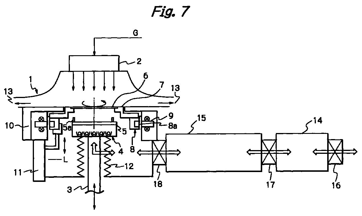
- Figs. 7 and 8 are diagrams showing a structural example of the substrate processing apparatus according to an embodiment of the present invention.
- reference numeral 1 denotes a substrate processing chamber.
- a processing gas supply unit 2 for supplying a raw material and other gas G is disposed at the upper side of the substrate processing chamber 1.
- a lamp heater 4 is disposed at the lower side of the substrate processing chamber 1. The lamp heater 4 is secured to the upper end of an elevating shaft 3. The lamp heater 4 is moved up and down by raising and lowering the elevating shaft 3 through an elevating mechanism (not shown).
- a transparent quartz plate 5 is disposed on the upper side of the lamp heater 4. The upper surface of the transparent quartz plate 5 is provided with a plurality of pins 5a for supporting a substrate 6 when the substrate 6 is loaded into and unloaded from the substrate processing chamber 1.
- Reference numeral 7 denotes an annular holder on which the substrate 6 is placed.
- the holder 7 is placed on an annular rotary member 8 (corresponding to a rotor) at the outer peripheral portion of the lower side of the holder 7.
- a stationary member 10 is disposed at the outer periphery of the substrate processing chamber 1.
- the stationary member 10 is provided with a magnetic rotational drive source 9 (corresponding to a stator).
- the holder 7 and the substrate 6 can be held at a predetermined position (a position where the upper surface of the stationary member 10 and the surface to be processed of the substrate 6 are flush with each other) due to magnetic coupling between the rotational drive source 9 and the target 8a of the rotary member 8, that magnetic coupling is provided by a static magnetic force generated by the magnetic rotational drive source 9.
- the rotary member 8 can be rotated by a rotating magnetic force generated by the rotational drive source 9.
- Reference numeral 11 denotes a holder elevating mechanism for raising and lowering the holder 7 via the rotary member 8. It should be noted that a plurality of holder elevating mechanisms 11 are provided circumferentially spaced from each other (an illustration of the other holder elevating mechanisms 11 is omitted) to support the rotary member 8 at a plurality of points.
- the holder elevating mechanisms 11 are synchronously operated to raise and lower the holder 7.
- a bellows 12 is disposed around the outer periphery of the elevating shaft 3. The bellows 12 expands and contracts in response to the up-and-down movement of the elevating shaft 3. Thus, provision of bellows 12 allows the elevating shaft 3 to be located outside the substrate processing chamber 1.
- exhaust systems 13 are connected to the substrate processing chamber 1.
- reference numeral 14 denotes a load-unload chamber
- reference numeral 15 denotes a robot chamber
- reference numeral 25 denotes a jig receiving chamber for receiving the holder 7 or holder 7 and the rotary member 8 therein, which will be explained later.
- Reference numerals 16, 17, 18, 26 and 27 denote gate valves, respectively.
- the elevating shaft 3 is lowered until the upper surface of the transparent quartz plate 5 is positioned below the level L shown in the figure. Subsequently, the holder 7 and the rotary member 8 are lowered with the holder elevating mechanisms 11 until the upper surface (substrate receiving surface) of the holder 7 reaches the position of level L for receiving the substrate 6 to be loaded into the substrate processing chamber 1 by the robot. At this time, the distal ends of the pins 5a provided on the upper surface of the transparent quartz plate 5 are positioned above the level L by a predetermined distance.
- the gate valve 16 is opened, a substrate 6 to be processed is loaded into the load-unload chamber 14. Upon completion of loading, the gate valve 16 is closed, and the load-unload chamber 14 is evacuated. The robot chamber 15 is maintained under a vacuum at all times.
- the gate valve 17 between the load-unload chamber 14 and the robot chamber 15 is opened, and the substrate 6 is taken out of the load-unload chamber 14 and moved into the robot chamber 15 by the arm of a robot installed in the robot chamber 15. Thereafter, the gate valve 17 between the robot chamber 15 and the load-unload chamber 14 is closed.
- the gate valve 18 between the substrate processing chamber 1 and the robot chamber 15 is opened, and the arm of the robot is extended to load the substrate 6 into the substrate processing chamber 1 and to place the substrate 6 onto the pins 5a provided on the upper surface of the transparent quartz plate 5. Then, the arm of the robot returns to the robot chamber 15, and the gate valve 18 is closed. In this state, the holder 7 and the rotary member 8 are raised by the holder elevating mechanisms 11. Consequently, the substrate 6 is placed on the holder 7, and the substrate 6, together with the holder 7, is further raised to the position illustrated in the figure. At this time, the annular rotary member 8 is held by means of the static magnetic force from the rotational drive source 9.
- the holder elevating mechanisms 11 is lowered by a predetermined distance to be separated from the rotary member 8.
- the lamp heater 4 is raised to the position illustrated in the figure, and the lamp is lit to heat the substrate 6.
- the rotational drive source 9 is activated to generate a rotating magnetic force to rotate the rotary member 8, thereby causing the substrate 6 to rotate about its center axis, together with the holder 7.
- the raw material and other gas G are supplied from the processing gas supply unit 2.
- an ascending heat convection is generated by the heated substrate 6 and holder 7, because the substrate 6 and the holder 7 are rotating to cause a pumping effect on the surface of the substrate as stated above, the flow of raw material and other processing gas G supplied downward from the processing gas supply unit 2 toward the substrate 6 overcomes the generated heat convection. Consequently, the processing gas can be smoothly supplied to the surface of the substrate 6, and the processing gas can be smoothly discharged in each sideward direction through the exhaust systems 13.
- the rotation of the rotary member 8 by means of the magnetic force generates by the rotational drive source 9 is terminated and subsequently the lamp heater 4 is lowered to its bottom position by lowering the elevator shaft 3.
- the holder elevating mechanism 11 is raised to support the holder 7 and the rotational drive source 9 is de-energized to release the magnetic coupling between the rotary member 8 and the rotational drive source 9.
- the holder 7 supporting the substrate 6 is lowered with the holder elevating mechanism 11 until the upper surface of the holder 7 reaches the position of level L for unloading the substrate 6 from the substrate processing chamber 1 to the load-and unload chamber 15.
- the gate valve 18 is opened and the substrate 6 is taken up from the holder 7 and moved from the substrate processing chamber 1 to the robot chamber 15 by the arm of the robot installed in the robot chamber 15. Then, the gate valve 18 is closed and the load-unload chamber 14 is evacuated until the pressure within the load-unload chamber reaches the vacuum level of the robot chamber 15, whereupon the gate valve 17 is opened and the substrate 6 is moved from the robot chamber 15 to the load-unload chamber 14 by the robot installed in the robot chamber 15, and then the gate valve 17 is closed.
- the holder 7 contaminated with deposits of the processing gas G is replaced.
- the substrate processing chamber 1 and the robot chamber 15 under a vacuum condition are supplied with a clean gas(inert gas) from a clean gas supply source(not shown) to place these chamber under the same pressure filled with the same clean gas.
- gate valve 18 is opened and the holder 7 within the substrate processing chamber 1 is taken up by the arm of the robot installed in the robot chamber 15 and transferred from the substrate processing chamber 1 to the robot chamber 15 and, then, the gate valve 18 is closed.
- the holder 7 is not fastened to the rotary member 8, but is simply placed thereon.
- a clean gas(inert gas) is supplied to the robot chamber 15 and a jig receiving chamber 25 from the clean gas supply source to place these chambers under the same pressure filled with the same clean gas.
- the gate valve 26 is opened and the holder 7 held by the robot in the robot chamber 15 is transferred from the robot chamber 15 to the jig receiving chamber 25 and, instead, a new holder 7 is taken out from the jig receiving chamber 25 and transferred to the robot chamber 15 by the robot and, then, the gate valve 26 is closed.
- a clean gas(inert gas) is supplied to the robot chamber 15 and the substrate processing chamber 1 from the clean gas supply source to place these chambers under the same pressure filled with the same clean gas. Then, the gate valve 18 is opened and the new holder 7 is placed on the predetermined position of the rotary member 8, which is then supported by the holder elevating mechanism 11 at its loading position.
- the processing of the substrate 6 in the substrate processing chamber 1 is resumed after the substrate processing chamber 1 is evacuated to a predetermined vacuum level by the exhaust system 13.
- the holder 7 received in the jig receiving chamber 25 is taken out from the jig receiving chamber 25 via a gate valve 27 and is subject to a cleaning operation for reuse.
- the rotary member 8 can also be loaded into and unloaded from the substrate processing chamber 1 by the robot installed in the robot chamber 15 or another loading-unloading mechanism (not shown), which is provided separately, to conduct a cleaning operation of the rotary member 8 unloaded from the substrate processing chamber 1.
- the rotary member 8 has an annular shape and the holder 7 having a hollow central portion is supported on the annular rotary member 8, the respective central portions of the rotary member 8 and the holder 7 are hollow. Consequently, the lamp heater 4 as a heat source can be disposed in the rotary member 8 under the substrate 6 so as to be parallel to the lower surface of the substrate 6.
- the pins 5a for supporting the substrate 6 when it is transferred can be provided on the transparent quartz plate 5.
- Fig. 9 is a diagram showing another structural example of a rotative holding mechanism for holding and rotating the holder 7 of the substrate processing apparatus according to the present invention.
- the rotative holding mechanism has a magnetic levitating member 19 (corresponding to the rotary member 8 in Fig. 7) made of a magnetic material.
- the holder 7 is incorporated into the upper part of the magnetic levitating member 19.
- the magnetic levitating member 19 is a cylindrical member having a collar portion 19a formed at the lower end thereof.
- the collar portion 19a extends horizontally outward.
- the stationary member 10 is provided with radial magnetic bearings 21 and 22 at upper and lower positions facing the outer periphery of the magnetic levitating member 19.
- the magnetic rotational drive source 9 is provided between the upper and lower radial magnetic bearings 21 and 22.
- An axial magnetic bearing 20 is disposed at a position facing the upper surface of the collar portion 19a.
- the radial magnetic bearing 21 comprises an electromagnet 21a and a displacement sensor 21b.
- the radial magnetic bearing 22 comprises an electromagnet 22a and a displacement sensor 22b.
- the axial magnetic bearing 20 comprises an electromagnet 20a and a displacement sensor 20b.
- a can 23 made of a non-magnetic material covers the respective surfaces of the electromagnet 21a and displacement sensor 21b of the radial magnetic bearing 21, the rotational drive source 9, the electromagnet 22a and displacement sensor 22b of the radial magnetic bearing 22 and the electromagnet 20a and displacement sensor 20b of the axial magnetic bearing 20.
- the surfaces of the electromagnets 21a, 22a and 20a, the displacement sensors 21b, 22b and 20b and the rotational drive source 9 are prevented from coming into contact with the processing gas and do not corrode.
- the surface of the stationary member 10 that is exposed in the substrate processing chamber 1 is covered with a quartz cover 24 to prevent contamination by the low material and other processing gas G.
- the assembly of the magnetic levitating member 19 and the holder 7 is adapted to be raised and lowered by holder elevating mechanisms (not shown) as in the case of Fig. 7.
- holder elevating mechanisms not shown
- the radial magnetic bearings 21 and 22 and the axial magnetic bearing 20 are activated to support the magnetic levitating member 19 in a levitational manner at the position illustrated in the figure.
- electromagnets are disposed at the upper and lower sides of a bearing target of a magnetic levitating member.
- the electromagnet 20a is provided only at the upper side, and the magnetic levitating member 19 is supported in a levitational manner by the balance of the magnetic force of the electromagnet 20a and the gravitational force acting on the holder 7 and the magnetic levitating member 19.
- the assembly of the holder 7 and the magnetic levitating member 19 can be lowered by the holder elevating mechanisms.
- the gap between the stationary member 10 and the magnetic levitating member 19 is detected with the displacement sensors 21b and 22b of the radial magnetic bearings 21 and 22 and the displacement sensor 20b of the axial magnetic bearing 20.
- the exciting currents of the electromagnets 21a, 22a and 20a are controlled to support the assembly of the holder 7 and the magnetic levitating member 19 in a levitational manner at a predetermined position as in the case of the conventional magnetic bearings.
- the magnetic levitating member 19 is supported by the magnetic bearings and rotated by a rotating magnetic force generated from the rotational drive source 9. Consequently, the holder 7 rotates together with the substrate 6. Loading and unloading of the substrate 6 are the same as in the substrate processing apparatus shown in Fig. 7. Therefore, a description thereof is omitted.
- the extent of heat convection produced by heating with the lamp heater 4 as a heat source depends on process parameters, i.e. temperature, molecular weight of gas, pressure, etc.
- process parameters i.e. temperature, molecular weight of gas, pressure, etc.
- uniformity of the processed surface of the substrate 6 and the processing speed differ according to the magnitude of the pumping effect produced by rotation of the substrate 6 and the holder 7.
- the processing speed also differs according to the kind of reaction precursor. Accordingly, the rotational speed at which the above-described effects can be produced by rotation of the substrate 6 and the holder 7 varies depending on the above-described parameters.
- the area of the substrate 6 and the processing gas flow rate are in proportional relation to each other, and the pumping effect produced by rotation of the substrate 6 and the holder 7 and the size of the substrate 6 are also in proportional relation to each other.
- the substrate 6 should preferably be rotated at about 50 to 150 rpm to cope with the problem of the ascending current (heat convection) generated from the upper surface of the substrate 6.
- a lamp heater (not shown) is disposed in the hollow portion of the magnetic levitating member 19 as a heat source. Therefore, the magnetic levitating member 19 has a large diameter. Accordingly, when the magnetic levitating member 19 is rotated, the peripheral speed at the outer peripheral portion of the magnetic levitating member 19 is high. Therefore, supporting the magnetic levitating member 19 with the magnetic bearings as shown in Fig. 9 (i.e. the radial magnetic bearings 21 and 22 and the axial magnetic bearing 20) is also favorable from the viewpoint of preventing the generation of particles.
- the apparatus when a substrate is processed in a reaction space where a processing gas is present under a vacuum such as exists in a substrate processing chamber, the substrate is levitated by the magnetic force source during processing. Consequently, the apparatus is free from problems such as the generation of particles.
- the holder can be held and released according to whether or not there is a magnetic coupling force from the magnetic force source, it becomes easy to perform the operation of holding and releasing the holder, and it also becomes easy to load and unload the holder into and from the substrate processing chamber. Accordingly, it becomes easy to carry out replacement of the holder and cleaning to remove a deposit, formed thereon.
- the holder is levitated and rotated by the magnetic force source. Consequently, a pumping effect produced by the rotation of the holder allows a flow of a processing gas descending toward the substrate to overcome the ascending current (heat convection) produced by heating. Accordingly, the processing gas reaches the substrate surface smoothly. Thus, efficient substrate processing can be realized.
- the magnetic levitating member supporting the holder is magnetically coupled to the magnetic force source. Therefore, when processing is not being carried out, the magnetic levitating member can freely move into or out of the substrate processing chamber. Accordingly, it becomes easy to perform the substrate loading-unloading operation and cleaning as well as replacement of the holder and the levitating member.
- the magnetic levitating member is supported in a levitational manner by the magnetic bearing and rotated by the magnetic rotational drive source. Therefore, it is possible to stably perform levitational support control and rotation control of the magnetic levitating member, even if it has a large diameter and rotates at a high peripheral speed.
Landscapes
- Chemical & Material Sciences (AREA)
- General Chemical & Material Sciences (AREA)
- Chemical Kinetics & Catalysis (AREA)
- Engineering & Computer Science (AREA)
- Materials Engineering (AREA)
- Mechanical Engineering (AREA)
- Metallurgy (AREA)
- Organic Chemistry (AREA)
- Container, Conveyance, Adherence, Positioning, Of Wafer (AREA)
- Drying Of Semiconductors (AREA)
Abstract
wherein, during processing of the substrate, the raw material for processing is supplied from a surface facing a surface to be processed of the substrate, and when the substrate and a holder on which the substrate is placed are moved to a predetermined position for processing in the substrate processing chamber, a space in the substrate processing chamber is divided by the substrate into an upper space serving as a reaction space for processing and a lower space where the substrate heating source, etc. are placed; and wherein the apparatus
Description
(heat convection) produced by heating. Accordingly, the processing gas reaches the substrate surface smoothly. Thus, efficient substrate processing can be realized.
Claims (5)
- A substrate processing apparatus comprising:a substrate processing chamber;a mechanism for loading and unloading a substrate;a substrate heating source;a holder for holding said substrate thereon; anda raw material supply source for supplying a raw material for processing;
wherein, the apparatus comprises a magnetic force source for holding said holder at the predetermined position in a levitational manner by a magnetic force during processing of said substrate. - A substrate processing apparatus comprising:a substrate processing chamber;a mechanism for loading and unloading a substrate into and out of said substrate processing chamber;a substrate heating source provided in said substrate processing chamber; anda raw material supply source for supplying a raw material toward said substrate for processing;
wherein, during processing of the substrate, said raw material for processing is supplied from a surface facing a surface to be processed of said substrate, and when said substrate and a holder on which said substrate is placed are moved to a predetermined position for processing in said substrate processing chamber, a space in said substrate processing chamber is divided by said substrate into an upper space serving as a reaction space for processing and a lower space where said substrate heating source, etc. are provided;andthe apparatus comprises a magnetic force source for holding said holder at a predetermined position in a levitational manner by a magnetic force during processing of said substrate. - A substrate processing apparatus according to claim 2, wherein said holder is rotated about a central axis of said substrate supported thereon by said magnetic force source during processing of said substrate.
- A substrate processing apparatus according to claim 2 or 3, wherein said holder is supported by an annular magnetic levitating member, said magnetic levitating member being magnetically coupled to said magnetic force source only when said holder is moved to the predetermined position for processing of said substrate.
- A substrate processing apparatus according to claim 4, wherein said magnetic force source includes magnetic bearings and a rotational drive source,said magnetic levitating member being supported in a levitational manner by said magnetic bearings and caused to rotate by a magnetic force provided by said rotational drive source.
Applications Claiming Priority (2)
| Application Number | Priority Date | Filing Date | Title |
|---|---|---|---|
| JP16828599 | 1999-06-15 | ||
| JP16828599 | 1999-06-15 |
Publications (3)
| Publication Number | Publication Date |
|---|---|
| EP1061557A2 true EP1061557A2 (en) | 2000-12-20 |
| EP1061557A3 EP1061557A3 (en) | 2005-09-21 |
| EP1061557B1 EP1061557B1 (en) | 2007-04-25 |
Family
ID=15865196
Family Applications (1)
| Application Number | Title | Priority Date | Filing Date |
|---|---|---|---|
| EP00112620A Expired - Lifetime EP1061557B1 (en) | 1999-06-15 | 2000-06-14 | Substrate processing apparatus |
Country Status (5)
| Country | Link |
|---|---|
| US (1) | US6464825B1 (en) |
| EP (1) | EP1061557B1 (en) |
| KR (1) | KR100710524B1 (en) |
| DE (1) | DE60034510T2 (en) |
| TW (1) | TW466576B (en) |
Cited By (2)
| Publication number | Priority date | Publication date | Assignee | Title |
|---|---|---|---|---|
| US7573745B2 (en) | 2002-07-10 | 2009-08-11 | Saifun Semiconductors Ltd. | Multiple use memory chip |
| US10229846B2 (en) | 2013-12-25 | 2019-03-12 | SCREEN Holdings Co., Ltd. | Substrate processing apparatus |
Families Citing this family (264)
| Publication number | Priority date | Publication date | Assignee | Title |
|---|---|---|---|---|
| AU5210300A (en) * | 1999-04-27 | 2000-11-10 | Gebruder Decker Gmbh & Co. Kg | Device for treating silicon wafers |
| US7018504B1 (en) * | 2000-09-11 | 2006-03-28 | Asm America, Inc. | Loadlock with integrated pre-clean chamber |
| US6770146B2 (en) * | 2001-02-02 | 2004-08-03 | Mattson Technology, Inc. | Method and system for rotating a semiconductor wafer in processing chambers |
| US6899507B2 (en) * | 2002-02-08 | 2005-05-31 | Asm Japan K.K. | Semiconductor processing apparatus comprising chamber partitioned into reaction and transfer sections |
| US6776849B2 (en) * | 2002-03-15 | 2004-08-17 | Asm America, Inc. | Wafer holder with peripheral lift ring |
| US7785456B2 (en) * | 2004-10-19 | 2010-08-31 | Jds Uniphase Corporation | Magnetic latch for a vapour deposition system |
| EP1630260B1 (en) * | 2004-08-20 | 2011-07-13 | JDS Uniphase Inc. | Magnetic latch for a vapour deposition system |
| US7954219B2 (en) * | 2004-08-20 | 2011-06-07 | Jds Uniphase Corporation | Substrate holder assembly device |
| JP5019811B2 (en) * | 2006-07-20 | 2012-09-05 | 東京エレクトロン株式会社 | Repair method of electrostatic adsorption electrode |
| EP1903603A3 (en) * | 2006-09-20 | 2009-09-16 | JDS Uniphase Corporation | Substrate holder assembly device |
| US7378618B1 (en) * | 2006-12-14 | 2008-05-27 | Applied Materials, Inc. | Rapid conductive cooling using a secondary process plane |
| WO2008140727A1 (en) * | 2007-05-08 | 2008-11-20 | Brooks Automation, Inc. | Substrate transport apparatus |
| US8440048B2 (en) * | 2009-01-28 | 2013-05-14 | Asm America, Inc. | Load lock having secondary isolation chamber |
| US8062384B2 (en) | 2009-06-12 | 2011-11-22 | Miasole | Systems, methods and apparatuses for magnetic processing of solar modules |
| US9105778B2 (en) * | 2009-06-12 | 2015-08-11 | Apollo Precision (Kunming) Yuanhong Limited | Systems methods and apparatuses for magnetic processing of solar modules |
| US20130023129A1 (en) | 2011-07-20 | 2013-01-24 | Asm America, Inc. | Pressure transmitter for a semiconductor processing environment |
| US20160376700A1 (en) | 2013-02-01 | 2016-12-29 | Asm Ip Holding B.V. | System for treatment of deposition reactor |
| US10403521B2 (en) * | 2013-03-13 | 2019-09-03 | Applied Materials, Inc. | Modular substrate heater for efficient thermal cycling |
| WO2015047639A1 (en) * | 2013-09-30 | 2015-04-02 | Applied Materials, Inc. | Support ring with encapsulated light barrier |
| CN103928317B (en) * | 2014-04-28 | 2016-10-26 | 北京七星华创电子股份有限公司 | Improve the method that technique sheet becomes film uniformity |
| US10858737B2 (en) | 2014-07-28 | 2020-12-08 | Asm Ip Holding B.V. | Showerhead assembly and components thereof |
| US10941490B2 (en) | 2014-10-07 | 2021-03-09 | Asm Ip Holding B.V. | Multiple temperature range susceptor, assembly, reactor and system including the susceptor, and methods of using the same |
| US10276355B2 (en) | 2015-03-12 | 2019-04-30 | Asm Ip Holding B.V. | Multi-zone reactor, system including the reactor, and method of using the same |
| US11139308B2 (en) | 2015-12-29 | 2021-10-05 | Asm Ip Holding B.V. | Atomic layer deposition of III-V compounds to form V-NAND devices |
| US9862006B2 (en) | 2015-12-29 | 2018-01-09 | Solarcity Corporation | Systems for levitating a metallic tray |
| US10529554B2 (en) | 2016-02-19 | 2020-01-07 | Asm Ip Holding B.V. | Method for forming silicon nitride film selectively on sidewalls or flat surfaces of trenches |
| US10343920B2 (en) | 2016-03-18 | 2019-07-09 | Asm Ip Holding B.V. | Aligned carbon nanotubes |
| US11453943B2 (en) | 2016-05-25 | 2022-09-27 | Asm Ip Holding B.V. | Method for forming carbon-containing silicon/metal oxide or nitride film by ALD using silicon precursor and hydrocarbon precursor |
| US10612137B2 (en) | 2016-07-08 | 2020-04-07 | Asm Ip Holdings B.V. | Organic reactants for atomic layer deposition |
| US9859151B1 (en) | 2016-07-08 | 2018-01-02 | Asm Ip Holding B.V. | Selective film deposition method to form air gaps |
| US9887082B1 (en) | 2016-07-28 | 2018-02-06 | Asm Ip Holding B.V. | Method and apparatus for filling a gap |
| US9812320B1 (en) | 2016-07-28 | 2017-11-07 | Asm Ip Holding B.V. | Method and apparatus for filling a gap |
| US11532757B2 (en) | 2016-10-27 | 2022-12-20 | Asm Ip Holding B.V. | Deposition of charge trapping layers |
| US10714350B2 (en) | 2016-11-01 | 2020-07-14 | ASM IP Holdings, B.V. | Methods for forming a transition metal niobium nitride film on a substrate by atomic layer deposition and related semiconductor device structures |
| KR102546317B1 (en) | 2016-11-15 | 2023-06-21 | 에이에스엠 아이피 홀딩 비.브이. | Gas supply unit and substrate processing apparatus including the same |
| US11447861B2 (en) | 2016-12-15 | 2022-09-20 | Asm Ip Holding B.V. | Sequential infiltration synthesis apparatus and a method of forming a patterned structure |
| US11581186B2 (en) | 2016-12-15 | 2023-02-14 | Asm Ip Holding B.V. | Sequential infiltration synthesis apparatus |
| US11390950B2 (en) | 2017-01-10 | 2022-07-19 | Asm Ip Holding B.V. | Reactor system and method to reduce residue buildup during a film deposition process |
| US10468261B2 (en) | 2017-02-15 | 2019-11-05 | Asm Ip Holding B.V. | Methods for forming a metallic film on a substrate by cyclical deposition and related semiconductor device structures |
| WO2018153479A1 (en) * | 2017-02-24 | 2018-08-30 | Applied Materials, Inc. | Carrier for use in a vacuum system, system for vacuum processing, and method for vacuum processing of a substrate |
| US10770286B2 (en) | 2017-05-08 | 2020-09-08 | Asm Ip Holdings B.V. | Methods for selectively forming a silicon nitride film on a substrate and related semiconductor device structures |
| US12040200B2 (en) | 2017-06-20 | 2024-07-16 | Asm Ip Holding B.V. | Semiconductor processing apparatus and methods for calibrating a semiconductor processing apparatus |
| US11306395B2 (en) | 2017-06-28 | 2022-04-19 | Asm Ip Holding B.V. | Methods for depositing a transition metal nitride film on a substrate by atomic layer deposition and related deposition apparatus |
| KR20190009245A (en) | 2017-07-18 | 2019-01-28 | 에이에스엠 아이피 홀딩 비.브이. | Methods for forming a semiconductor device structure and related semiconductor device structures |
| US11374112B2 (en) | 2017-07-19 | 2022-06-28 | Asm Ip Holding B.V. | Method for depositing a group IV semiconductor and related semiconductor device structures |
| US10590535B2 (en) | 2017-07-26 | 2020-03-17 | Asm Ip Holdings B.V. | Chemical treatment, deposition and/or infiltration apparatus and method for using the same |
| TWI815813B (en) | 2017-08-04 | 2023-09-21 | 荷蘭商Asm智慧財產控股公司 | Showerhead assembly for distributing a gas within a reaction chamber |
| US10692741B2 (en) | 2017-08-08 | 2020-06-23 | Asm Ip Holdings B.V. | Radiation shield |
| US10770336B2 (en) | 2017-08-08 | 2020-09-08 | Asm Ip Holding B.V. | Substrate lift mechanism and reactor including same |
| US11769682B2 (en) | 2017-08-09 | 2023-09-26 | Asm Ip Holding B.V. | Storage apparatus for storing cassettes for substrates and processing apparatus equipped therewith |
| US11830730B2 (en) | 2017-08-29 | 2023-11-28 | Asm Ip Holding B.V. | Layer forming method and apparatus |
| US11295980B2 (en) | 2017-08-30 | 2022-04-05 | Asm Ip Holding B.V. | Methods for depositing a molybdenum metal film over a dielectric surface of a substrate by a cyclical deposition process and related semiconductor device structures |
| US10658205B2 (en) | 2017-09-28 | 2020-05-19 | Asm Ip Holdings B.V. | Chemical dispensing apparatus and methods for dispensing a chemical to a reaction chamber |
| US10403504B2 (en) | 2017-10-05 | 2019-09-03 | Asm Ip Holding B.V. | Method for selectively depositing a metallic film on a substrate |
| US10923344B2 (en) | 2017-10-30 | 2021-02-16 | Asm Ip Holding B.V. | Methods for forming a semiconductor structure and related semiconductor structures |
| CN111316417B (en) | 2017-11-27 | 2023-12-22 | 阿斯莫Ip控股公司 | Storage device for use with batch furnaces for storing wafer cassettes |
| JP7206265B2 (en) | 2017-11-27 | 2023-01-17 | エーエスエム アイピー ホールディング ビー.ブイ. | Equipment with a clean mini-environment |
| US10872771B2 (en) | 2018-01-16 | 2020-12-22 | Asm Ip Holding B. V. | Method for depositing a material film on a substrate within a reaction chamber by a cyclical deposition process and related device structures |
| CN111630203A (en) | 2018-01-19 | 2020-09-04 | Asm Ip私人控股有限公司 | Method of depositing a gap fill layer by plasma assisted deposition |
| TWI799494B (en) | 2018-01-19 | 2023-04-21 | 荷蘭商Asm 智慧財產控股公司 | Deposition method |
| US11081345B2 (en) | 2018-02-06 | 2021-08-03 | Asm Ip Holding B.V. | Method of post-deposition treatment for silicon oxide film |
| JP7124098B2 (en) | 2018-02-14 | 2022-08-23 | エーエスエム・アイピー・ホールディング・ベー・フェー | Method for depositing a ruthenium-containing film on a substrate by a cyclical deposition process |
| US10896820B2 (en) | 2018-02-14 | 2021-01-19 | Asm Ip Holding B.V. | Method for depositing a ruthenium-containing film on a substrate by a cyclical deposition process |
| US10731249B2 (en) | 2018-02-15 | 2020-08-04 | Asm Ip Holding B.V. | Method of forming a transition metal containing film on a substrate by a cyclical deposition process, a method for supplying a transition metal halide compound to a reaction chamber, and related vapor deposition apparatus |
| KR102636427B1 (en) | 2018-02-20 | 2024-02-13 | 에이에스엠 아이피 홀딩 비.브이. | Substrate processing method and apparatus |
| US10975470B2 (en) | 2018-02-23 | 2021-04-13 | Asm Ip Holding B.V. | Apparatus for detecting or monitoring for a chemical precursor in a high temperature environment |
| US11473195B2 (en) | 2018-03-01 | 2022-10-18 | Asm Ip Holding B.V. | Semiconductor processing apparatus and a method for processing a substrate |
| DE102018116526A1 (en) | 2018-03-15 | 2019-09-19 | Dürr Systems Ag | Separation stage and separation unit with at least one separation stage |
| KR102646467B1 (en) | 2018-03-27 | 2024-03-11 | 에이에스엠 아이피 홀딩 비.브이. | Method of forming an electrode on a substrate and a semiconductor device structure including an electrode |
| KR102600229B1 (en) | 2018-04-09 | 2023-11-10 | 에이에스엠 아이피 홀딩 비.브이. | Substrate supporting device, substrate processing apparatus including the same and substrate processing method |
| US12025484B2 (en) | 2018-05-08 | 2024-07-02 | Asm Ip Holding B.V. | Thin film forming method |
| US12272527B2 (en) | 2018-05-09 | 2025-04-08 | Asm Ip Holding B.V. | Apparatus for use with hydrogen radicals and method of using same |
| KR102596988B1 (en) | 2018-05-28 | 2023-10-31 | 에이에스엠 아이피 홀딩 비.브이. | Method of processing a substrate and a device manufactured by the same |
| US11718913B2 (en) | 2018-06-04 | 2023-08-08 | Asm Ip Holding B.V. | Gas distribution system and reactor system including same |
| US10797133B2 (en) | 2018-06-21 | 2020-10-06 | Asm Ip Holding B.V. | Method for depositing a phosphorus doped silicon arsenide film and related semiconductor device structures |
| KR102568797B1 (en) | 2018-06-21 | 2023-08-21 | 에이에스엠 아이피 홀딩 비.브이. | Substrate processing system |
| US11499222B2 (en) | 2018-06-27 | 2022-11-15 | Asm Ip Holding B.V. | Cyclic deposition methods for forming metal-containing material and films and structures including the metal-containing material |
| KR20250134000A (en) | 2018-06-27 | 2025-09-09 | 에이에스엠 아이피 홀딩 비.브이. | Cyclic deposition methods for forming metal-containing material and films and structures including the metal-containing material |
| US10388513B1 (en) | 2018-07-03 | 2019-08-20 | Asm Ip Holding B.V. | Method for depositing silicon-free carbon-containing film as gap-fill layer by pulse plasma-assisted deposition |
| US10755922B2 (en) | 2018-07-03 | 2020-08-25 | Asm Ip Holding B.V. | Method for depositing silicon-free carbon-containing film as gap-fill layer by pulse plasma-assisted deposition |
| US11053591B2 (en) | 2018-08-06 | 2021-07-06 | Asm Ip Holding B.V. | Multi-port gas injection system and reactor system including same |
| US11430674B2 (en) | 2018-08-22 | 2022-08-30 | Asm Ip Holding B.V. | Sensor array, apparatus for dispensing a vapor phase reactant to a reaction chamber and related methods |
| KR102707956B1 (en) | 2018-09-11 | 2024-09-19 | 에이에스엠 아이피 홀딩 비.브이. | Method for deposition of a thin film |
| US11024523B2 (en) | 2018-09-11 | 2021-06-01 | Asm Ip Holding B.V. | Substrate processing apparatus and method |
| CN110970344B (en) | 2018-10-01 | 2024-10-25 | Asmip控股有限公司 | Substrate holding device, system including the same and method of using the same |
| KR102592699B1 (en) | 2018-10-08 | 2023-10-23 | 에이에스엠 아이피 홀딩 비.브이. | Substrate support unit and apparatuses for depositing thin film and processing the substrate including the same |
| KR102546322B1 (en) | 2018-10-19 | 2023-06-21 | 에이에스엠 아이피 홀딩 비.브이. | Substrate processing apparatus and substrate processing method |
| KR102605121B1 (en) * | 2018-10-19 | 2023-11-23 | 에이에스엠 아이피 홀딩 비.브이. | Substrate processing apparatus and substrate processing method |
| US12378665B2 (en) | 2018-10-26 | 2025-08-05 | Asm Ip Holding B.V. | High temperature coatings for a preclean and etch apparatus and related methods |
| US11087997B2 (en) | 2018-10-31 | 2021-08-10 | Asm Ip Holding B.V. | Substrate processing apparatus for processing substrates |
| KR102748291B1 (en) | 2018-11-02 | 2024-12-31 | 에이에스엠 아이피 홀딩 비.브이. | Substrate support unit and substrate processing apparatus including the same |
| US11572620B2 (en) | 2018-11-06 | 2023-02-07 | Asm Ip Holding B.V. | Methods for selectively depositing an amorphous silicon film on a substrate |
| US10818758B2 (en) | 2018-11-16 | 2020-10-27 | Asm Ip Holding B.V. | Methods for forming a metal silicate film on a substrate in a reaction chamber and related semiconductor device structures |
| US12040199B2 (en) | 2018-11-28 | 2024-07-16 | Asm Ip Holding B.V. | Substrate processing apparatus for processing substrates |
| US11217444B2 (en) | 2018-11-30 | 2022-01-04 | Asm Ip Holding B.V. | Method for forming an ultraviolet radiation responsive metal oxide-containing film |
| KR102636428B1 (en) | 2018-12-04 | 2024-02-13 | 에이에스엠 아이피 홀딩 비.브이. | A method for cleaning a substrate processing apparatus |
| US11158513B2 (en) | 2018-12-13 | 2021-10-26 | Asm Ip Holding B.V. | Methods for forming a rhenium-containing film on a substrate by a cyclical deposition process and related semiconductor device structures |
| JP7504584B2 (en) | 2018-12-14 | 2024-06-24 | エーエスエム・アイピー・ホールディング・ベー・フェー | Method and system for forming device structures using selective deposition of gallium nitride - Patents.com |
| JP7155999B2 (en) * | 2018-12-20 | 2022-10-19 | 株式会社島津製作所 | Vacuum valves and valve controllers |
| TWI819180B (en) | 2019-01-17 | 2023-10-21 | 荷蘭商Asm 智慧財產控股公司 | Methods of forming a transition metal containing film on a substrate by a cyclical deposition process |
| KR102638425B1 (en) | 2019-02-20 | 2024-02-21 | 에이에스엠 아이피 홀딩 비.브이. | Method and apparatus for filling a recess formed within a substrate surface |
| US11482533B2 (en) | 2019-02-20 | 2022-10-25 | Asm Ip Holding B.V. | Apparatus and methods for plug fill deposition in 3-D NAND applications |
| TWI845607B (en) | 2019-02-20 | 2024-06-21 | 荷蘭商Asm Ip私人控股有限公司 | Cyclical deposition method and apparatus for filling a recess formed within a substrate surface |
| TWI842826B (en) | 2019-02-22 | 2024-05-21 | 荷蘭商Asm Ip私人控股有限公司 | Substrate processing apparatus and method for processing substrate |
| KR102858005B1 (en) | 2019-03-08 | 2025-09-09 | 에이에스엠 아이피 홀딩 비.브이. | Method for Selective Deposition of Silicon Nitride Layer and Structure Including Selectively-Deposited Silicon Nitride Layer |
| KR102762833B1 (en) | 2019-03-08 | 2025-02-04 | 에이에스엠 아이피 홀딩 비.브이. | STRUCTURE INCLUDING SiOCN LAYER AND METHOD OF FORMING SAME |
| US11538716B2 (en) * | 2019-03-22 | 2022-12-27 | Kokusai Electric Corporation | Substrate processing apparatus, method of manufacturing semiconductor device, and recording medium |
| JP2020167398A (en) | 2019-03-28 | 2020-10-08 | エーエスエム・アイピー・ホールディング・ベー・フェー | Door openers and substrate processing equipment provided with door openers |
| KR102809999B1 (en) | 2019-04-01 | 2025-05-19 | 에이에스엠 아이피 홀딩 비.브이. | Method of manufacturing semiconductor device |
| US11447864B2 (en) | 2019-04-19 | 2022-09-20 | Asm Ip Holding B.V. | Layer forming method and apparatus |
| KR20200125453A (en) | 2019-04-24 | 2020-11-04 | 에이에스엠 아이피 홀딩 비.브이. | Gas-phase reactor system and method of using same |
| KR102929471B1 (en) | 2019-05-07 | 2026-02-20 | 에이에스엠 아이피 홀딩 비.브이. | Chemical source vessel with dip tube |
| KR102929472B1 (en) | 2019-05-10 | 2026-02-20 | 에이에스엠 아이피 홀딩 비.브이. | Method of depositing material onto a surface and structure formed according to the method |
| JP7598201B2 (en) | 2019-05-16 | 2024-12-11 | エーエスエム・アイピー・ホールディング・ベー・フェー | Wafer boat handling apparatus, vertical batch furnace and method |
| JP7612342B2 (en) | 2019-05-16 | 2025-01-14 | エーエスエム・アイピー・ホールディング・ベー・フェー | Wafer boat handling apparatus, vertical batch furnace and method |
| USD947913S1 (en) | 2019-05-17 | 2022-04-05 | Asm Ip Holding B.V. | Susceptor shaft |
| USD975665S1 (en) | 2019-05-17 | 2023-01-17 | Asm Ip Holding B.V. | Susceptor shaft |
| KR20200141003A (en) | 2019-06-06 | 2020-12-17 | 에이에스엠 아이피 홀딩 비.브이. | Gas-phase reactor system including a gas detector |
| KR102918757B1 (en) | 2019-06-10 | 2026-01-28 | 에이에스엠 아이피 홀딩 비.브이. | Method for cleaning quartz epitaxial chambers |
| KR20200143254A (en) | 2019-06-11 | 2020-12-23 | 에이에스엠 아이피 홀딩 비.브이. | Method of forming an electronic structure using an reforming gas, system for performing the method, and structure formed using the method |
| KR102911421B1 (en) | 2019-07-03 | 2026-01-12 | 에이에스엠 아이피 홀딩 비.브이. | Temperature control assembly for substrate processing apparatus and method of using same |
| JP7499079B2 (en) | 2019-07-09 | 2024-06-13 | エーエスエム・アイピー・ホールディング・ベー・フェー | Plasma device using coaxial waveguide and substrate processing method |
| CN112216646B (en) | 2019-07-10 | 2026-02-10 | Asmip私人控股有限公司 | Substrate support assembly and substrate processing apparatus including the thereof |
| KR102895115B1 (en) | 2019-07-16 | 2025-12-03 | 에이에스엠 아이피 홀딩 비.브이. | Substrate processing apparatus |
| KR102955799B1 (en) | 2019-07-17 | 2026-04-21 | 에이에스엠 아이피 홀딩 비.브이. | Radical assist ignition plasma system and method |
| KR102860110B1 (en) | 2019-07-17 | 2025-09-16 | 에이에스엠 아이피 홀딩 비.브이. | Methods of forming silicon germanium structures |
| US11643724B2 (en) | 2019-07-18 | 2023-05-09 | Asm Ip Holding B.V. | Method of forming structures using a neutral beam |
| KR102903090B1 (en) | 2019-07-19 | 2025-12-19 | 에이에스엠 아이피 홀딩 비.브이. | Method of Forming Topology-Controlled Amorphous Carbon Polymer Film |
| TWI851767B (en) | 2019-07-29 | 2024-08-11 | 荷蘭商Asm Ip私人控股有限公司 | Methods for selective deposition utilizing n-type dopants and/or alternative dopants to achieve high dopant incorporation |
| CN112309900B (en) | 2019-07-30 | 2025-11-04 | Asmip私人控股有限公司 | Substrate processing equipment |
| KR20210015655A (en) | 2019-07-30 | 2021-02-10 | 에이에스엠 아이피 홀딩 비.브이. | Substrate processing apparatus and method |
| CN112309899B (en) | 2019-07-30 | 2025-11-14 | Asmip私人控股有限公司 | Substrate processing equipment |
| US11587815B2 (en) | 2019-07-31 | 2023-02-21 | Asm Ip Holding B.V. | Vertical batch furnace assembly |
| US12622218B2 (en) | 2019-07-31 | 2026-05-05 | Asm Ip Holding B.V. | Cassette lid opening device |
| US11227782B2 (en) | 2019-07-31 | 2022-01-18 | Asm Ip Holding B.V. | Vertical batch furnace assembly |
| US11587814B2 (en) | 2019-07-31 | 2023-02-21 | Asm Ip Holding B.V. | Vertical batch furnace assembly |
| CN112323048B (en) | 2019-08-05 | 2024-02-09 | Asm Ip私人控股有限公司 | Liquid level sensor for chemical source container |
| KR20210018761A (en) | 2019-08-09 | 2021-02-18 | 에이에스엠 아이피 홀딩 비.브이. | heater assembly including cooling apparatus and method of using same |
| USD965044S1 (en) | 2019-08-19 | 2022-09-27 | Asm Ip Holding B.V. | Susceptor shaft |
| USD965524S1 (en) | 2019-08-19 | 2022-10-04 | Asm Ip Holding B.V. | Susceptor support |
| JP7810514B2 (en) | 2019-08-21 | 2026-02-03 | エーエスエム・アイピー・ホールディング・ベー・フェー | Film-forming raw material mixed gas generating device and film-forming device |
| USD979506S1 (en) | 2019-08-22 | 2023-02-28 | Asm Ip Holding B.V. | Insulator |
| KR20210024423A (en) | 2019-08-22 | 2021-03-05 | 에이에스엠 아이피 홀딩 비.브이. | Method for forming a structure with a hole |
| US11286558B2 (en) | 2019-08-23 | 2022-03-29 | Asm Ip Holding B.V. | Methods for depositing a molybdenum nitride film on a surface of a substrate by a cyclical deposition process and related semiconductor device structures including a molybdenum nitride film |
| KR102928101B1 (en) | 2019-08-23 | 2026-02-13 | 에이에스엠 아이피 홀딩 비.브이. | Method for depositing silicon oxide film having improved quality by peald using bis(diethylamino)silane |
| CN112442674A (en) | 2019-09-03 | 2021-03-05 | Asm Ip私人控股有限公司 | Method and apparatus for depositing chalcogenide films and structures including films |
| KR102806450B1 (en) | 2019-09-04 | 2025-05-12 | 에이에스엠 아이피 홀딩 비.브이. | Methods for selective deposition using a sacrificial capping layer |
| KR102733104B1 (en) | 2019-09-05 | 2024-11-22 | 에이에스엠 아이피 홀딩 비.브이. | Substrate processing apparatus |
| US12469693B2 (en) | 2019-09-17 | 2025-11-11 | Asm Ip Holding B.V. | Method of forming a carbon-containing layer and structure including the layer |
| US11562901B2 (en) | 2019-09-25 | 2023-01-24 | Asm Ip Holding B.V. | Substrate processing method |
| CN112593212B (en) | 2019-10-02 | 2023-12-22 | Asm Ip私人控股有限公司 | Method for forming topologically selective silicon oxide film through cyclic plasma enhanced deposition process |
| US12428726B2 (en) | 2019-10-08 | 2025-09-30 | Asm Ip Holding B.V. | Gas injection system and reactor system including same |
| TWI846953B (en) | 2019-10-08 | 2024-07-01 | 荷蘭商Asm Ip私人控股有限公司 | Substrate processing device |
| KR102948143B1 (en) | 2019-10-08 | 2026-04-07 | 에이에스엠 아이피 홀딩 비.브이. | Reactor system including a gas distribution assembly for use with activated species and method of using same |
| TWI846966B (en) | 2019-10-10 | 2024-07-01 | 荷蘭商Asm Ip私人控股有限公司 | Method of forming a photoresist underlayer and structure including same |
| US12009241B2 (en) | 2019-10-14 | 2024-06-11 | Asm Ip Holding B.V. | Vertical batch furnace assembly with detector to detect cassette |
| TWI834919B (en) | 2019-10-16 | 2024-03-11 | 荷蘭商Asm Ip私人控股有限公司 | Method of topology-selective film formation of silicon oxide |
| US11637014B2 (en) | 2019-10-17 | 2023-04-25 | Asm Ip Holding B.V. | Methods for selective deposition of doped semiconductor material |
| KR102845724B1 (en) | 2019-10-21 | 2025-08-13 | 에이에스엠 아이피 홀딩 비.브이. | Apparatus and methods for selectively etching films |
| US11996292B2 (en) | 2019-10-25 | 2024-05-28 | Asm Ip Holding B.V. | Methods for filling a gap feature on a substrate surface and related semiconductor structures |
| US11646205B2 (en) | 2019-10-29 | 2023-05-09 | Asm Ip Holding B.V. | Methods of selectively forming n-type doped material on a surface, systems for selectively forming n-type doped material, and structures formed using same |
| KR102890638B1 (en) | 2019-11-05 | 2025-11-25 | 에이에스엠 아이피 홀딩 비.브이. | Structures with doped semiconductor layers and methods and systems for forming same |
| US11501968B2 (en) | 2019-11-15 | 2022-11-15 | Asm Ip Holding B.V. | Method for providing a semiconductor device with silicon filled gaps |
| KR102861314B1 (en) | 2019-11-20 | 2025-09-17 | 에이에스엠 아이피 홀딩 비.브이. | Method of depositing carbon-containing material on a surface of a substrate, structure formed using the method, and system for forming the structure |
| KR20210065848A (en) | 2019-11-26 | 2021-06-04 | 에이에스엠 아이피 홀딩 비.브이. | Methods for selectivley forming a target film on a substrate comprising a first dielectric surface and a second metallic surface |
| CN112951697B (en) | 2019-11-26 | 2025-07-29 | Asmip私人控股有限公司 | Substrate processing apparatus |
| CN120432376A (en) | 2019-11-29 | 2025-08-05 | Asm Ip私人控股有限公司 | Substrate processing equipment |
| CN120998766A (en) | 2019-11-29 | 2025-11-21 | Asm Ip私人控股有限公司 | Substrate processing equipment |
| JP7527928B2 (en) | 2019-12-02 | 2024-08-05 | エーエスエム・アイピー・ホールディング・ベー・フェー | Substrate processing apparatus and substrate processing method |
| KR20210070898A (en) | 2019-12-04 | 2021-06-15 | 에이에스엠 아이피 홀딩 비.브이. | Substrate processing apparatus |
| JP7703317B2 (en) | 2019-12-17 | 2025-07-07 | エーエスエム・アイピー・ホールディング・ベー・フェー | Methods for forming vanadium nitride layers and structures including vanadium nitride layers - Patents.com |
| KR102943768B1 (en) | 2019-12-19 | 2026-03-26 | 에이에스엠 아이피 홀딩 비.브이. | Methods for filling a gap feature on a substrate and related semiconductor structures |
| TWI901623B (en) | 2020-01-06 | 2025-10-21 | 荷蘭商Asm Ip私人控股有限公司 | Gas supply assembly and valve plate assembly |
| TWI887322B (en) | 2020-01-06 | 2025-06-21 | 荷蘭商Asm Ip私人控股有限公司 | Reactor system, lift pin, and processing method |
| US11993847B2 (en) | 2020-01-08 | 2024-05-28 | Asm Ip Holding B.V. | Injector |
| KR102882467B1 (en) | 2020-01-16 | 2025-11-05 | 에이에스엠 아이피 홀딩 비.브이. | Method of forming high aspect ratio features |
| KR102675856B1 (en) | 2020-01-20 | 2024-06-17 | 에이에스엠 아이피 홀딩 비.브이. | Method of forming thin film and method of modifying surface of thin film |
| TWI889744B (en) | 2020-01-29 | 2025-07-11 | 荷蘭商Asm Ip私人控股有限公司 | Contaminant trap system, and baffle plate stack |
| TWI871421B (en) | 2020-02-03 | 2025-02-01 | 荷蘭商Asm Ip私人控股有限公司 | Devices and structures including a vanadium or indium layer and methods and systems for forming the same |
| KR20210100010A (en) | 2020-02-04 | 2021-08-13 | 에이에스엠 아이피 홀딩 비.브이. | Method and apparatus for transmittance measurements of large articles |
| US11776846B2 (en) | 2020-02-07 | 2023-10-03 | Asm Ip Holding B.V. | Methods for depositing gap filling fluids and related systems and devices |
| KR102916725B1 (en) | 2020-02-13 | 2026-01-23 | 에이에스엠 아이피 홀딩 비.브이. | Substrate processing apparatus including light receiving device and calibration method of light receiving device |
| KR20210103953A (en) | 2020-02-13 | 2021-08-24 | 에이에스엠 아이피 홀딩 비.브이. | Gas distribution assembly and method of using same |
| US11781243B2 (en) | 2020-02-17 | 2023-10-10 | Asm Ip Holding B.V. | Method for depositing low temperature phosphorous-doped silicon |
| TWI895326B (en) | 2020-02-28 | 2025-09-01 | 荷蘭商Asm Ip私人控股有限公司 | System dedicated for parts cleaning |
| TWI914330B (en) | 2020-03-04 | 2026-02-11 | 荷蘭商Asm Ip私人控股有限公司 | Reactor system, and alignment fixture |
| KR20210116249A (en) | 2020-03-11 | 2021-09-27 | 에이에스엠 아이피 홀딩 비.브이. | lockout tagout assembly and system and method of using same |
| KR20210116240A (en) | 2020-03-11 | 2021-09-27 | 에이에스엠 아이피 홀딩 비.브이. | Substrate handling device with adjustable joints |
| CN113394086A (en) | 2020-03-12 | 2021-09-14 | Asm Ip私人控股有限公司 | Method for producing a layer structure having a target topological profile |
| US12173404B2 (en) | 2020-03-17 | 2024-12-24 | Asm Ip Holding B.V. | Method of depositing epitaxial material, structure formed using the method, and system for performing the method |
| KR102755229B1 (en) | 2020-04-02 | 2025-01-14 | 에이에스엠 아이피 홀딩 비.브이. | Thin film forming method |
| TWI887376B (en) | 2020-04-03 | 2025-06-21 | 荷蘭商Asm Ip私人控股有限公司 | Method for manufacturing semiconductor device |
| TWI888525B (en) | 2020-04-08 | 2025-07-01 | 荷蘭商Asm Ip私人控股有限公司 | Apparatus and methods for selectively etching silcon oxide films |
| KR20210127620A (en) | 2020-04-13 | 2021-10-22 | 에이에스엠 아이피 홀딩 비.브이. | method of forming a nitrogen-containing carbon film and system for performing the method |
| US11821078B2 (en) | 2020-04-15 | 2023-11-21 | Asm Ip Holding B.V. | Method for forming precoat film and method for forming silicon-containing film |
| KR20210128343A (en) | 2020-04-15 | 2021-10-26 | 에이에스엠 아이피 홀딩 비.브이. | Method of forming chromium nitride layer and structure including the chromium nitride layer |
| US11996289B2 (en) | 2020-04-16 | 2024-05-28 | Asm Ip Holding B.V. | Methods of forming structures including silicon germanium and silicon layers, devices formed using the methods, and systems for performing the methods |
| KR102901748B1 (en) | 2020-04-21 | 2025-12-17 | 에이에스엠 아이피 홀딩 비.브이. | Method for processing a substrate |
| KR20210132612A (en) | 2020-04-24 | 2021-11-04 | 에이에스엠 아이피 홀딩 비.브이. | Methods and apparatus for stabilizing vanadium compounds |
| KR102934380B1 (en) | 2020-04-24 | 2026-03-05 | 에이에스엠 아이피 홀딩 비.브이. | Methods of forming structures including vanadium boride and vanadium phosphide layers |
| US11898243B2 (en) | 2020-04-24 | 2024-02-13 | Asm Ip Holding B.V. | Method of forming vanadium nitride-containing layer |
| KR102866804B1 (en) | 2020-04-24 | 2025-09-30 | 에이에스엠 아이피 홀딩 비.브이. | Vertical batch furnace assembly comprising a cooling gas supply |
| KR20210132600A (en) | 2020-04-24 | 2021-11-04 | 에이에스엠 아이피 홀딩 비.브이. | Methods and systems for depositing a layer comprising vanadium, nitrogen, and a further element |
| KR102783898B1 (en) | 2020-04-29 | 2025-03-18 | 에이에스엠 아이피 홀딩 비.브이. | Solid source precursor vessel |
| KR20210134869A (en) | 2020-05-01 | 2021-11-11 | 에이에스엠 아이피 홀딩 비.브이. | Fast FOUP swapping with a FOUP handler |
| JP7726664B2 (en) | 2020-05-04 | 2025-08-20 | エーエスエム・アイピー・ホールディング・ベー・フェー | Substrate processing system for processing a substrate |
| JP7736446B2 (en) | 2020-05-07 | 2025-09-09 | エーエスエム・アイピー・ホールディング・ベー・フェー | Reactor system with tuned circuit |
| KR20210137395A (en) | 2020-05-07 | 2021-11-17 | 에이에스엠 아이피 홀딩 비.브이. | Apparatus and methods for performing an in-situ etch of reaction chambers with fluorine-based radicals |
| KR102788543B1 (en) | 2020-05-13 | 2025-03-27 | 에이에스엠 아이피 홀딩 비.브이. | Laser alignment fixture for a reactor system |
| TWI915365B (en) | 2020-05-15 | 2026-02-21 | 荷蘭商Asm Ip私人控股有限公司 | Method of forming a silicon germanium layer, semiconductor structure, semiconductor device, method of forming a deposition layer, and deposition system |
| TWI911214B (en) | 2020-05-19 | 2026-01-11 | 荷蘭商Asm Ip私人控股有限公司 | Substrate processing apparatus |
| KR20210145079A (en) | 2020-05-21 | 2021-12-01 | 에이에스엠 아이피 홀딩 비.브이. | Flange and apparatus for processing substrates |
| KR102795476B1 (en) | 2020-05-21 | 2025-04-11 | 에이에스엠 아이피 홀딩 비.브이. | Structures including multiple carbon layers and methods of forming and using same |
| TWI873343B (en) | 2020-05-22 | 2025-02-21 | 荷蘭商Asm Ip私人控股有限公司 | Reaction system for forming thin film on substrate |
| KR20210146802A (en) | 2020-05-26 | 2021-12-06 | 에이에스엠 아이피 홀딩 비.브이. | Method for depositing boron and gallium containing silicon germanium layers |
| TWI876048B (en) | 2020-05-29 | 2025-03-11 | 荷蘭商Asm Ip私人控股有限公司 | Substrate processing device |
| TW202212620A (en) | 2020-06-02 | 2022-04-01 | 荷蘭商Asm Ip私人控股有限公司 | Apparatus for processing substrate, method of forming film, and method of controlling apparatus for processing substrate |
| KR20210156219A (en) | 2020-06-16 | 2021-12-24 | 에이에스엠 아이피 홀딩 비.브이. | Method for depositing boron containing silicon germanium layers |
| TWI908816B (en) | 2020-06-24 | 2025-12-21 | 荷蘭商Asm Ip私人控股有限公司 | Method for forming a layer provided with silicon |
| TWI873359B (en) | 2020-06-30 | 2025-02-21 | 荷蘭商Asm Ip私人控股有限公司 | Substrate processing method |
| TW202202649A (en) | 2020-07-08 | 2022-01-16 | 荷蘭商Asm Ip私人控股有限公司 | Substrate processing method |
| TWI864307B (en) | 2020-07-17 | 2024-12-01 | 荷蘭商Asm Ip私人控股有限公司 | Structures, methods and systems for use in photolithography |
| TWI878570B (en) | 2020-07-20 | 2025-04-01 | 荷蘭商Asm Ip私人控股有限公司 | Method and system for depositing molybdenum layers |
| KR20220011092A (en) | 2020-07-20 | 2022-01-27 | 에이에스엠 아이피 홀딩 비.브이. | Method and system for forming structures including transition metal layers |
| US12322591B2 (en) | 2020-07-27 | 2025-06-03 | Asm Ip Holding B.V. | Thin film deposition process |
| TW202605918A (en) | 2020-08-11 | 2026-02-01 | 荷蘭商Asm Ip私人控股有限公司 | Gate stack |
| KR102915124B1 (en) | 2020-08-14 | 2026-01-19 | 에이에스엠 아이피 홀딩 비.브이. | Method for processing a substrate |
| US12040177B2 (en) | 2020-08-18 | 2024-07-16 | Asm Ip Holding B.V. | Methods for forming a laminate film by cyclical plasma-enhanced deposition processes |
| TWI911263B (en) | 2020-08-25 | 2026-01-11 | 荷蘭商Asm Ip私人控股有限公司 | Method for cleaning a substrate, method for selectively depositing, and reaction system |
| US11725280B2 (en) | 2020-08-26 | 2023-08-15 | Asm Ip Holding B.V. | Method for forming metal silicon oxide and metal silicon oxynitride layers |
| TWI911265B (en) | 2020-08-27 | 2026-01-11 | 荷蘭商Asm Ip私人控股有限公司 | Method of forming patterned structures, method of manipulating mechanical property, and device structure |
| USD990534S1 (en) | 2020-09-11 | 2023-06-27 | Asm Ip Holding B.V. | Weighted lift pin |
| KR20220036866A (en) | 2020-09-16 | 2022-03-23 | 에이에스엠 아이피 홀딩 비.브이. | Silicon oxide deposition method |
| USD1012873S1 (en) | 2020-09-24 | 2024-01-30 | Asm Ip Holding B.V. | Electrode for semiconductor processing apparatus |
| TWI889903B (en) | 2020-09-25 | 2025-07-11 | 荷蘭商Asm Ip私人控股有限公司 | Semiconductor processing method |
| US12009224B2 (en) | 2020-09-29 | 2024-06-11 | Asm Ip Holding B.V. | Apparatus and method for etching metal nitrides |
| KR20220045900A (en) | 2020-10-06 | 2022-04-13 | 에이에스엠 아이피 홀딩 비.브이. | Deposition method and an apparatus for depositing a silicon-containing material |
| CN114388427A (en) | 2020-10-06 | 2022-04-22 | Asm Ip私人控股有限公司 | Method and system for forming silicon nitride on sidewalls of features |
| CN114293174A (en) | 2020-10-07 | 2022-04-08 | Asm Ip私人控股有限公司 | Gas supply unit and substrate processing apparatus including the same |
| KR102855834B1 (en) | 2020-10-14 | 2025-09-04 | 에이에스엠 아이피 홀딩 비.브이. | Method of Depositing Material on Stepped Structure |
| KR102873665B1 (en) | 2020-10-15 | 2025-10-17 | 에이에스엠 아이피 홀딩 비.브이. | Method of manufacturing semiconductor device, and substrate treatment apparatus using ether-cat |
| TW202217037A (en) | 2020-10-22 | 2022-05-01 | 荷蘭商Asm Ip私人控股有限公司 | Method of depositing vanadium metal, structure, device and a deposition assembly |
| TW202223136A (en) | 2020-10-28 | 2022-06-16 | 荷蘭商Asm Ip私人控股有限公司 | Method for forming layer on substrate, and semiconductor processing system |
| TW202229620A (en) | 2020-11-12 | 2022-08-01 | 特文特大學 | Deposition system, method for controlling reaction condition, method for depositing |
| TW202229795A (en) | 2020-11-23 | 2022-08-01 | 荷蘭商Asm Ip私人控股有限公司 | A substrate processing apparatus with an injector |
| TW202235649A (en) | 2020-11-24 | 2022-09-16 | 荷蘭商Asm Ip私人控股有限公司 | Methods for filling a gap and related systems and devices |
| KR20220076343A (en) | 2020-11-30 | 2022-06-08 | 에이에스엠 아이피 홀딩 비.브이. | an injector configured for arrangement within a reaction chamber of a substrate processing apparatus |
| KR20220077875A (en) | 2020-12-02 | 2022-06-09 | 에이에스엠 아이피 홀딩 비.브이. | Cleaning fixture for showerhead assemblies |
| US12255053B2 (en) | 2020-12-10 | 2025-03-18 | Asm Ip Holding B.V. | Methods and systems for depositing a layer |
| US12159788B2 (en) | 2020-12-14 | 2024-12-03 | Asm Ip Holding B.V. | Method of forming structures for threshold voltage control |
| US11946137B2 (en) | 2020-12-16 | 2024-04-02 | Asm Ip Holding B.V. | Runout and wobble measurement fixtures |
| TW202232639A (en) | 2020-12-18 | 2022-08-16 | 荷蘭商Asm Ip私人控股有限公司 | Wafer processing apparatus with a rotatable table |
| KR20220090438A (en) | 2020-12-22 | 2022-06-29 | 에이에스엠 아이피 홀딩 비.브이. | Transition metal deposition method |
| KR20220090435A (en) | 2020-12-22 | 2022-06-29 | 에이에스엠 아이피 홀딩 비.브이. | Precursor capsule, vessel and method |
| TW202226899A (en) | 2020-12-22 | 2022-07-01 | 荷蘭商Asm Ip私人控股有限公司 | Plasma treatment device having matching box |
| USD980814S1 (en) | 2021-05-11 | 2023-03-14 | Asm Ip Holding B.V. | Gas distributor for substrate processing apparatus |
| USD1023959S1 (en) | 2021-05-11 | 2024-04-23 | Asm Ip Holding B.V. | Electrode for substrate processing apparatus |
| USD981973S1 (en) | 2021-05-11 | 2023-03-28 | Asm Ip Holding B.V. | Reactor wall for substrate processing apparatus |
| USD980813S1 (en) | 2021-05-11 | 2023-03-14 | Asm Ip Holding B.V. | Gas flow control plate for substrate processing apparatus |
| USD990441S1 (en) | 2021-09-07 | 2023-06-27 | Asm Ip Holding B.V. | Gas flow control plate |
| USD1099184S1 (en) | 2021-11-29 | 2025-10-21 | Asm Ip Holding B.V. | Weighted lift pin |
| USD1060598S1 (en) | 2021-12-03 | 2025-02-04 | Asm Ip Holding B.V. | Split showerhead cover |
| CN114649256A (en) * | 2022-03-18 | 2022-06-21 | 北京北方华创微电子装备有限公司 | Rotary base device and semiconductor process equipment |
| CN117467962B (en) * | 2023-12-28 | 2024-03-08 | 上海陛通半导体能源科技股份有限公司 | Thin film deposition apparatus |
Family Cites Families (17)
| Publication number | Priority date | Publication date | Assignee | Title |
|---|---|---|---|---|
| JP3096073B2 (en) | 1991-03-05 | 2000-10-10 | 株式会社東芝 | Vapor phase growth apparatus and method |
| JPH0570287A (en) | 1991-09-10 | 1993-03-23 | Toshiba Mach Co Ltd | Heating equipment for wafer for vapor phase growth |
| JPH05152207A (en) | 1991-11-28 | 1993-06-18 | Toshiba Mach Co Ltd | Vapor growth method |
| US5273588A (en) | 1992-06-15 | 1993-12-28 | Materials Research Corporation | Semiconductor wafer processing CVD reactor apparatus comprising contoured electrode gas directing means |
| US5444217A (en) | 1993-01-21 | 1995-08-22 | Moore Epitaxial Inc. | Rapid thermal processing apparatus for processing semiconductor wafers |
| JPH0758036A (en) * | 1993-08-16 | 1995-03-03 | Ebara Corp | Thin film forming equipment |
| JPH07273053A (en) | 1994-03-31 | 1995-10-20 | Tokyo Electron Ltd | Processing apparatus and aluminum-based member coating method |
| JPH08255792A (en) | 1995-03-16 | 1996-10-01 | Toshiba Corp | Method for manufacturing semiconductor device |
| JPH093650A (en) | 1995-06-16 | 1997-01-07 | Ebara Corp | Vapor growth device for thin film |
| JPH093648A (en) | 1995-06-16 | 1997-01-07 | Ebara Corp | Vapor growth device for thin film |
| JPH093649A (en) | 1995-06-16 | 1997-01-07 | Ebara Corp | Vapor growth device for thin film |
| TW331652B (en) * | 1995-06-16 | 1998-05-11 | Ebara Corp | Thin film vapor deposition apparatus |
| JPH0931656A (en) | 1995-07-24 | 1997-02-04 | Ebara Corp | Thin film vapor growth apparatus |
| JPH0953181A (en) | 1995-08-11 | 1997-02-25 | Ebara Corp | Thin film vapor growth device |
| US5795448A (en) * | 1995-12-08 | 1998-08-18 | Sony Corporation | Magnetic device for rotating a substrate |
| WO1997031389A1 (en) * | 1996-02-23 | 1997-08-28 | Tokyo Electron Limited | Heat treatment device |
| US5879128A (en) * | 1996-07-24 | 1999-03-09 | Applied Materials, Inc. | Lift pin and support pin apparatus for a processing chamber |
-
2000
- 2000-06-05 TW TW089110939A patent/TW466576B/en not_active IP Right Cessation
- 2000-06-14 DE DE60034510T patent/DE60034510T2/en not_active Expired - Fee Related
- 2000-06-14 EP EP00112620A patent/EP1061557B1/en not_active Expired - Lifetime
- 2000-06-14 KR KR1020000032620A patent/KR100710524B1/en not_active Expired - Fee Related
- 2000-06-15 US US09/593,709 patent/US6464825B1/en not_active Expired - Fee Related
Cited By (2)
| Publication number | Priority date | Publication date | Assignee | Title |
|---|---|---|---|---|
| US7573745B2 (en) | 2002-07-10 | 2009-08-11 | Saifun Semiconductors Ltd. | Multiple use memory chip |
| US10229846B2 (en) | 2013-12-25 | 2019-03-12 | SCREEN Holdings Co., Ltd. | Substrate processing apparatus |
Also Published As
| Publication number | Publication date |
|---|---|
| DE60034510T2 (en) | 2008-01-03 |
| EP1061557B1 (en) | 2007-04-25 |
| TW466576B (en) | 2001-12-01 |
| DE60034510D1 (en) | 2007-06-06 |
| KR100710524B1 (en) | 2007-04-23 |
| US6464825B1 (en) | 2002-10-15 |
| KR20010020987A (en) | 2001-03-15 |
| EP1061557A3 (en) | 2005-09-21 |
Similar Documents
| Publication | Publication Date | Title |
|---|---|---|
| US6464825B1 (en) | Substrate processing apparatus including a magnetically levitated and rotated substrate holder | |
| JP5001432B2 (en) | Substrate processing apparatus and substrate processing method | |
| KR102556368B1 (en) | Transfer hand and substrate processing apparatus | |
| KR20200102612A (en) | Substrate treating apparatus and substrate treating method | |
| JP5090536B2 (en) | Substrate processing method and substrate processing apparatus | |
| JPH1092916A (en) | Lift pin and support pin device for processing chamber | |
| KR20210030917A (en) | Substrate treating apparatus and substrate treating method | |
| KR102872406B1 (en) | Support unit, and apparatus for treating substrate with the same | |
| CN101681867B (en) | Treating apparatus | |
| CN116547794A (en) | Device for rotating a substrate | |
| JP3916851B2 (en) | Substrate processing equipment | |
| JP2008258477A (en) | Processing apparatus and atmosphere replacement method | |
| EP0634784A1 (en) | Variable speed wafer exchange robot | |
| JP4241513B2 (en) | Substrate processing apparatus and processing method | |
| KR101361300B1 (en) | Substrate processing apparatus | |
| JP3414449B2 (en) | Transfer device | |
| JPH10244201A (en) | Base plate treatment apparatus | |
| JP2006049489A (en) | Substrate processing equipment | |
| JP5031960B2 (en) | Substrate processing apparatus and semiconductor device manufacturing method | |
| KR102558421B1 (en) | Transfer hand and substrate processing apparatus | |
| JPH04267355A (en) | Wafer conveying robot | |
| TWI910536B (en) | Substrate holding device and substrate treating apparatus provided therewith | |
| KR20210085973A (en) | Apparatus and method for treating substrate | |
| JP7398988B2 (en) | sputtering equipment | |
| JP4963678B2 (en) | Atmosphere replacement method |
Legal Events
| Date | Code | Title | Description |
|---|---|---|---|
| PUAI | Public reference made under article 153(3) epc to a published international application that has entered the european phase |
Free format text: ORIGINAL CODE: 0009012 |
|
| AK | Designated contracting states |
Kind code of ref document: A2 Designated state(s): AT BE CH CY DE DK ES FI FR GB GR IE IT LI LU MC NL PT SE |
|
| AX | Request for extension of the european patent |
Free format text: AL;LT;LV;MK;RO;SI |
|
| PUAL | Search report despatched |
Free format text: ORIGINAL CODE: 0009013 |
|
| AK | Designated contracting states |
Kind code of ref document: A3 Designated state(s): AT BE CH CY DE DK ES FI FR GB GR IE IT LI LU MC NL PT SE |
|
| AX | Request for extension of the european patent |
Extension state: AL LT LV MK RO SI |
|
| RIC1 | Information provided on ipc code assigned before grant |
Ipc: 7H 01L 21/00 A Ipc: 7C 23C 16/458 B Ipc: 7H 01L 21/68 B Ipc: 7B 05C 11/08 B |
|
| 17P | Request for examination filed |
Effective date: 20060320 |
|
| AKX | Designation fees paid |
Designated state(s): DE FR GB |
|
| GRAP | Despatch of communication of intention to grant a patent |
Free format text: ORIGINAL CODE: EPIDOSNIGR1 |
|
| GRAS | Grant fee paid |
Free format text: ORIGINAL CODE: EPIDOSNIGR3 |
|
| GRAA | (expected) grant |
Free format text: ORIGINAL CODE: 0009210 |
|
| AK | Designated contracting states |
Kind code of ref document: B1 Designated state(s): DE FR GB |
|
| REG | Reference to a national code |
Ref country code: GB Ref legal event code: FG4D |
|
| REF | Corresponds to: |
Ref document number: 60034510 Country of ref document: DE Date of ref document: 20070606 Kind code of ref document: P |
|
| PLBE | No opposition filed within time limit |
Free format text: ORIGINAL CODE: 0009261 |
|
| STAA | Information on the status of an ep patent application or granted ep patent |
Free format text: STATUS: NO OPPOSITION FILED WITHIN TIME LIMIT |
|
| GBPC | Gb: european patent ceased through non-payment of renewal fee |
Effective date: 20070725 |
|
| 26N | No opposition filed |
Effective date: 20080128 |
|
| PG25 | Lapsed in a contracting state [announced via postgrant information from national office to epo] |
Ref country code: GB Free format text: LAPSE BECAUSE OF NON-PAYMENT OF DUE FEES Effective date: 20070725 |
|
| PGFP | Annual fee paid to national office [announced via postgrant information from national office to epo] |
Ref country code: DE Payment date: 20080625 Year of fee payment: 9 |
|
| REG | Reference to a national code |
Ref country code: FR Ref legal event code: ST Effective date: 20100226 |
|
| PG25 | Lapsed in a contracting state [announced via postgrant information from national office to epo] |
Ref country code: FR Free format text: LAPSE BECAUSE OF NON-PAYMENT OF DUE FEES Effective date: 20090630 |
|
| PGFP | Annual fee paid to national office [announced via postgrant information from national office to epo] |
Ref country code: FR Payment date: 20080423 Year of fee payment: 9 |
|
| PG25 | Lapsed in a contracting state [announced via postgrant information from national office to epo] |
Ref country code: DE Free format text: LAPSE BECAUSE OF NON-PAYMENT OF DUE FEES Effective date: 20100101 |