EP1058379A2 - Gegentaktanordnung - Google Patents
Gegentaktanordnung Download PDFInfo
- Publication number
- EP1058379A2 EP1058379A2 EP00109778A EP00109778A EP1058379A2 EP 1058379 A2 EP1058379 A2 EP 1058379A2 EP 00109778 A EP00109778 A EP 00109778A EP 00109778 A EP00109778 A EP 00109778A EP 1058379 A2 EP1058379 A2 EP 1058379A2
- Authority
- EP
- European Patent Office
- Prior art keywords
- transistors
- trl1
- transistor
- push
- characteristic impedance
- Prior art date
- Legal status (The legal status is an assumption and is not a legal conclusion. Google has not performed a legal analysis and makes no representation as to the accuracy of the status listed.)
- Granted
Links
Images
Classifications
-
- H—ELECTRICITY
- H03—ELECTRONIC CIRCUITRY
- H03D—DEMODULATION OR TRANSFERENCE OF MODULATION FROM ONE CARRIER TO ANOTHER
- H03D7/00—Transference of modulation from one carrier to another, e.g. frequency-changing
- H03D7/14—Balanced arrangements
Definitions
- the application relates to a push-pull arrangement for use in frequency multipliers, reception mixers, Signal converters or modulators after the Work push-pull principle and those with the fundamental wave or a subharmonic of the local oscillator be controlled according to the generic term of Claim 1.
- the object of the invention is with as little as possible Component effort the power of the signal from Split local / local oscillator so that the Transistors with the same power and 180 ° Phase shift to each other are controlled, and that the signal despite specimen scatter of the transistor parameters well decoupled from the other signal gates of the circuit is.
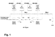
- the object of the invention is that similar to a traveling wave amplifier (but here reduced to two transistors), the characteristic impedance of the Detour line, or for larger bandwidth requirements the wave resistance of a single or multi-stage hybrid, selected to match the transistor input resistors becomes. in addition there is a terminating resistor on the second Transistor provided either directly or with connected to a line with a suitable characteristic impedance is. A pre-adjustment of the Transistor input impedances can be made.
- the advantage of the invention is that specimen scatter no longer has a direct effect on strong adaptation changes within a resonance structure, but rather, within a certain range of specimen scatter, mainly cause a slight change in the phase position of the control signals.
- a further advantageous embodiment of the invention results in the event that the control inputs of the transistors T1 and T2 are provided by means of a circuit for matching the input impedance. This is aimed at an additional compensation of possible sample variations of the transistors T1 and T2 .
- the exemplary embodiment described above relates on the realization of the invention Push-pull arrangement with field effect transistors, but it is naturally also conceivable in a corresponding manner a push-pull arrangement with other types of transistors (e.g. bipolar transistors).
Landscapes
- Engineering & Computer Science (AREA)
- Power Engineering (AREA)
- Amplifiers (AREA)
- Inductance-Capacitance Distribution Constants And Capacitance-Resistance Oscillators (AREA)
- Superheterodyne Receivers (AREA)
- Oscillators With Electromechanical Resonators (AREA)
- Electronic Switches (AREA)
Abstract
Description

wobei ZTRLx die Wellenwiderstände der Leitungen TRL1 und TRL2 sind. Dabei ist zu beachten, daß in der Praxis ZTRL1 und ZTRL2 im allgemeinen nicht genau gleich sind, da auf Grund von Verzweigungen und speziellen Geometrien innerhalb des Schaltungslayouts zu Impedanzverschiebungen kommen kann.
wobei TRL1 der Phasenverschiebung zwischen den Steuereingängen der beiden Transistoren T1 und T2 entspricht. Hierbei ist bei Dimensionierung von TRL1 jedoch auch u.a. die Transistor Eingangsimpedanz und die Leitungsgeometrie zwischen den Transistoren und TRL1 zu beachten.
Claims (2)
- Gegentaktanordnung bei welcher die Leistung des Signals vom Überlagerungs-/Lokaloszillators so aufgeteilt wird, daß die beiden Transistoren mit gleicher Leistung und 180° phasenverschoben ausgesteuert werden, dadurch gekennzeichnet,daß der Wellenwiderstand der Umwegleitung, bzw. bei größerer Bandbreitenanforderungen der Wellenwiderstand eines ein- oder mehrstufigen Hybrids, passend zu den Transistor-Eingangswiderständen und dem Schaltungslayout gewählt wird,und daß ein Abschlußwiderstand am zweiten Transistor vorgesehen wird, der entweder unmittelbar oder über eine Leitung mit passendem Wellenwiderstand angeschlossen ist.
- Gegentaktanordnung nach Anspruch 1, dadurch gekennzeichnet, daß die Steuereingänge der Transistoren mittels einer Schaltung zur Eingangsimpedanzanpassung versehen werden
Applications Claiming Priority (2)
| Application Number | Priority Date | Filing Date | Title |
|---|---|---|---|
| DE19924716 | 1999-05-31 | ||
| DE19924716A DE19924716A1 (de) | 1999-05-31 | 1999-05-31 | Gegentaktanordnung |
Publications (3)
| Publication Number | Publication Date |
|---|---|
| EP1058379A2 true EP1058379A2 (de) | 2000-12-06 |
| EP1058379A3 EP1058379A3 (de) | 2003-02-12 |
| EP1058379B1 EP1058379B1 (de) | 2010-09-08 |
Family
ID=7909634
Family Applications (1)
| Application Number | Title | Priority Date | Filing Date |
|---|---|---|---|
| EP00109778A Expired - Lifetime EP1058379B1 (de) | 1999-05-31 | 2000-05-09 | Gegentaktanordnung |
Country Status (4)
| Country | Link |
|---|---|
| US (1) | US6437659B1 (de) |
| EP (1) | EP1058379B1 (de) |
| AT (1) | ATE480903T1 (de) |
| DE (2) | DE19924716A1 (de) |
Citations (1)
| Publication number | Priority date | Publication date | Assignee | Title |
|---|---|---|---|---|
| WO1997041644A1 (en) | 1996-04-29 | 1997-11-06 | Motorola Inc. | Method and apparatus for mixing signals |
Family Cites Families (6)
| Publication number | Priority date | Publication date | Assignee | Title |
|---|---|---|---|---|
| JPS58173906A (ja) * | 1982-04-06 | 1983-10-12 | Fujitsu Ltd | 周波数変換器 |
| US4660006A (en) * | 1985-04-15 | 1987-04-21 | Raytheon Company | Radio frequency multiplier producing an even harmonic output |
| US4992761A (en) * | 1989-03-06 | 1991-02-12 | Motorola, Inc. | Passive 180 degree broadband MMIC hybrid |
| US5008894A (en) * | 1990-03-30 | 1991-04-16 | Synrad, Incorporated | Drive system for RF-excited gas lasers |
| JPH05243853A (ja) * | 1992-03-02 | 1993-09-21 | Fujitsu Ltd | 周波数逓倍器 |
| WO1999018661A1 (de) * | 1997-10-08 | 1999-04-15 | Siemens Aktiengesellschaft | Gegentaktmischer |
-
1999
- 1999-05-31 DE DE19924716A patent/DE19924716A1/de not_active Withdrawn
-
2000
- 2000-05-09 EP EP00109778A patent/EP1058379B1/de not_active Expired - Lifetime
- 2000-05-09 DE DE50015985T patent/DE50015985D1/de not_active Expired - Lifetime
- 2000-05-09 AT AT00109778T patent/ATE480903T1/de active
- 2000-05-31 US US09/584,509 patent/US6437659B1/en not_active Expired - Fee Related
Patent Citations (1)
| Publication number | Priority date | Publication date | Assignee | Title |
|---|---|---|---|---|
| WO1997041644A1 (en) | 1996-04-29 | 1997-11-06 | Motorola Inc. | Method and apparatus for mixing signals |
Also Published As
| Publication number | Publication date |
|---|---|
| DE19924716A1 (de) | 2000-12-07 |
| US6437659B1 (en) | 2002-08-20 |
| EP1058379A3 (de) | 2003-02-12 |
| ATE480903T1 (de) | 2010-09-15 |
| DE50015985D1 (de) | 2010-10-21 |
| EP1058379B1 (de) | 2010-09-08 |
Similar Documents
| Publication | Publication Date | Title |
|---|---|---|
| DE69707903T2 (de) | Verwendung von zirkulatoren in zeitduplex-funksystemen | |
| EP2035840B1 (de) | Verfahren zum betreiben einer anordnung zum bestimmen der betriebskenngrössen eines hochfrequenz-leistungsverstärkers | |
| DE69920486T2 (de) | Halbleiterschaltung | |
| DE3612657C2 (de) | Frequenzumsetzungseinrichtung | |
| DE102007029957A1 (de) | Ultraschallsensor mit reziproker Sende- und Empfangsschaltung | |
| DE2255207A1 (de) | Anordnung zum ableiten des fehlersignals in einem system zum selbsttaetigen nachfuehren einer mikrowellenantenne | |
| EP0061582B1 (de) | Verfahren und Schaltungsanordnung zur Kompensation der Nichtlinearitäten von Übertragungsgliedern in einem Richtfunkübertragungssystem | |
| EP0683539A1 (de) | Mikrowellenleitungsstruktur | |
| DE19901751B4 (de) | Mehrfachüberlagerungsstufe für einen Empfänger oder Spektrumanalysator | |
| EP2013638A1 (de) | Balancierter serienmischer für hochfrequenzsignale | |
| DE10344876B3 (de) | Signalverarbeitungseinrichtung, insbesondere für den Mobilfunk | |
| EP1058379A2 (de) | Gegentaktanordnung | |
| DE102010002575A1 (de) | Rauscharmer Mischer | |
| DE102009027327A1 (de) | Mischerbaugruppe und Radarsensor für Kraftfahrzeuge | |
| WO1999004282A1 (de) | Einrichtung zum senden und empfangen von radarwellen, insbesondere für einen abstandssensor | |
| DE102009004832A1 (de) | Mischer mit balanciertem lokalen Oszillatorsignal | |
| DE3004019C2 (de) | Einrichtung zur Frequenzumwandlung für einen Mikrowellen-Empfänger oder -Sender | |
| EP1017124A1 (de) | Leistungsteiler für Hochfrequenzsignale | |
| DE10000225B4 (de) | Integrierte Mikrowellen/Millimeterwellenschaltung | |
| EP0674383A1 (de) | Schaltungsanordnung zum Liefern eines Signalwechselstromes | |
| EP0687062A1 (de) | Analoger Phasenschieber für kleine Steuerspannungen | |
| WO1999018661A1 (de) | Gegentaktmischer | |
| DE19921438B4 (de) | Überlagerungsstufe für Hochfrequenzempfänger | |
| DE880902C (de) | Anordnung zur Speisung eines Hochfrequenzverbrauchers durch zwei Hochfrequenzquellen | |
| DE102006044006B4 (de) | Vorrichtung zum Wandeln eines asymmetrischen Singals in ein Differenzsignal |
Legal Events
| Date | Code | Title | Description |
|---|---|---|---|
| PUAI | Public reference made under article 153(3) epc to a published international application that has entered the european phase |
Free format text: ORIGINAL CODE: 0009012 |
|
| AK | Designated contracting states |
Kind code of ref document: A2 Designated state(s): AT BE CH CY DE DK ES FI FR GB GR IE IT LI LU MC NL PT SE |
|
| AX | Request for extension of the european patent |
Free format text: AL;LT;LV;MK;RO;SI |
|
| RAP1 | Party data changed (applicant data changed or rights of an application transferred) |
Owner name: EADS DEUTSCHLAND GMBH |
|
| PUAL | Search report despatched |
Free format text: ORIGINAL CODE: 0009013 |
|
| AK | Designated contracting states |
Designated state(s): AT BE CH CY DE DK ES FI FR GB GR IE IT LI LU MC NL PT SE |
|
| AX | Request for extension of the european patent |
Extension state: AL LT LV MK RO SI |
|
| 17P | Request for examination filed |
Effective date: 20030717 |
|
| AKX | Designation fees paid |
Designated state(s): AT BE CH CY DE DK ES FI FR GB GR IE IT LI LU MC NL PT SE |
|
| 17Q | First examination report despatched |
Effective date: 20070712 |
|
| GRAP | Despatch of communication of intention to grant a patent |
Free format text: ORIGINAL CODE: EPIDOSNIGR1 |
|
| RTI1 | Title (correction) |
Free format text: PUSH PULL DEVICE |
|
| GRAS | Grant fee paid |
Free format text: ORIGINAL CODE: EPIDOSNIGR3 |
|
| GRAA | (expected) grant |
Free format text: ORIGINAL CODE: 0009210 |
|
| AK | Designated contracting states |
Kind code of ref document: B1 Designated state(s): AT BE CH CY DE DK ES FI FR GB GR IE IT LI LU MC NL PT SE |
|
| REG | Reference to a national code |
Ref country code: GB Ref legal event code: FG4D Free format text: NOT ENGLISH |
|
| REG | Reference to a national code |
Ref country code: CH Ref legal event code: EP |
|
| REG | Reference to a national code |
Ref country code: IE Ref legal event code: FG4D Free format text: LANGUAGE OF EP DOCUMENT: GERMAN |
|
| REF | Corresponds to: |
Ref document number: 50015985 Country of ref document: DE Date of ref document: 20101021 Kind code of ref document: P |
|
| REG | Reference to a national code |
Ref country code: NL Ref legal event code: VDEP Effective date: 20100908 |
|
| PG25 | Lapsed in a contracting state [announced via postgrant information from national office to epo] |
Ref country code: CY Free format text: LAPSE BECAUSE OF FAILURE TO SUBMIT A TRANSLATION OF THE DESCRIPTION OR TO PAY THE FEE WITHIN THE PRESCRIBED TIME-LIMIT Effective date: 20100908 |
|
| REG | Reference to a national code |
Ref country code: IE Ref legal event code: FD4D |
|
| PG25 | Lapsed in a contracting state [announced via postgrant information from national office to epo] |
Ref country code: GR Free format text: LAPSE BECAUSE OF FAILURE TO SUBMIT A TRANSLATION OF THE DESCRIPTION OR TO PAY THE FEE WITHIN THE PRESCRIBED TIME-LIMIT Effective date: 20101209 Ref country code: NL Free format text: LAPSE BECAUSE OF FAILURE TO SUBMIT A TRANSLATION OF THE DESCRIPTION OR TO PAY THE FEE WITHIN THE PRESCRIBED TIME-LIMIT Effective date: 20100908 Ref country code: SE Free format text: LAPSE BECAUSE OF FAILURE TO SUBMIT A TRANSLATION OF THE DESCRIPTION OR TO PAY THE FEE WITHIN THE PRESCRIBED TIME-LIMIT Effective date: 20100908 |
|
| PG25 | Lapsed in a contracting state [announced via postgrant information from national office to epo] |
Ref country code: IE Free format text: LAPSE BECAUSE OF FAILURE TO SUBMIT A TRANSLATION OF THE DESCRIPTION OR TO PAY THE FEE WITHIN THE PRESCRIBED TIME-LIMIT Effective date: 20100908 |
|
| PG25 | Lapsed in a contracting state [announced via postgrant information from national office to epo] |
Ref country code: PT Free format text: LAPSE BECAUSE OF FAILURE TO SUBMIT A TRANSLATION OF THE DESCRIPTION OR TO PAY THE FEE WITHIN THE PRESCRIBED TIME-LIMIT Effective date: 20110110 |
|
| PG25 | Lapsed in a contracting state [announced via postgrant information from national office to epo] |
Ref country code: ES Free format text: LAPSE BECAUSE OF FAILURE TO SUBMIT A TRANSLATION OF THE DESCRIPTION OR TO PAY THE FEE WITHIN THE PRESCRIBED TIME-LIMIT Effective date: 20101219 |
|
| PLBE | No opposition filed within time limit |
Free format text: ORIGINAL CODE: 0009261 |
|
| STAA | Information on the status of an ep patent application or granted ep patent |
Free format text: STATUS: NO OPPOSITION FILED WITHIN TIME LIMIT |
|
| 26N | No opposition filed |
Effective date: 20110609 |
|
| PG25 | Lapsed in a contracting state [announced via postgrant information from national office to epo] |
Ref country code: DK Free format text: LAPSE BECAUSE OF FAILURE TO SUBMIT A TRANSLATION OF THE DESCRIPTION OR TO PAY THE FEE WITHIN THE PRESCRIBED TIME-LIMIT Effective date: 20100908 |
|
| REG | Reference to a national code |
Ref country code: DE Ref legal event code: R097 Ref document number: 50015985 Country of ref document: DE Effective date: 20110609 |
|
| BERE | Be: lapsed |
Owner name: EADS DEUTSCHLAND G.M.B.H. Effective date: 20110531 |
|
| PG25 | Lapsed in a contracting state [announced via postgrant information from national office to epo] |
Ref country code: MC Free format text: LAPSE BECAUSE OF NON-PAYMENT OF DUE FEES Effective date: 20110531 |
|
| REG | Reference to a national code |
Ref country code: CH Ref legal event code: PL |
|
| GBPC | Gb: european patent ceased through non-payment of renewal fee |
Effective date: 20110509 |
|
| PG25 | Lapsed in a contracting state [announced via postgrant information from national office to epo] |
Ref country code: FI Free format text: LAPSE BECAUSE OF NON-PAYMENT OF DUE FEES Effective date: 20110509 Ref country code: LI Free format text: LAPSE BECAUSE OF NON-PAYMENT OF DUE FEES Effective date: 20110531 Ref country code: CH Free format text: LAPSE BECAUSE OF NON-PAYMENT OF DUE FEES Effective date: 20110531 |
|
| REG | Reference to a national code |
Ref country code: FR Ref legal event code: ST Effective date: 20120131 |
|
| PG25 | Lapsed in a contracting state [announced via postgrant information from national office to epo] |
Ref country code: IT Free format text: LAPSE BECAUSE OF NON-PAYMENT OF DUE FEES Effective date: 20110509 |
|
| REG | Reference to a national code |
Ref country code: DE Ref legal event code: R119 Ref document number: 50015985 Country of ref document: DE Effective date: 20111201 |
|
| PG25 | Lapsed in a contracting state [announced via postgrant information from national office to epo] |
Ref country code: BE Free format text: LAPSE BECAUSE OF NON-PAYMENT OF DUE FEES Effective date: 20110531 |
|
| PG25 | Lapsed in a contracting state [announced via postgrant information from national office to epo] |
Ref country code: FR Free format text: LAPSE BECAUSE OF NON-PAYMENT OF DUE FEES Effective date: 20110531 |
|
| PG25 | Lapsed in a contracting state [announced via postgrant information from national office to epo] |
Ref country code: GB Free format text: LAPSE BECAUSE OF NON-PAYMENT OF DUE FEES Effective date: 20110509 |
|
| REG | Reference to a national code |
Ref country code: AT Ref legal event code: MM01 Ref document number: 480903 Country of ref document: AT Kind code of ref document: T Effective date: 20110509 |
|
| PG25 | Lapsed in a contracting state [announced via postgrant information from national office to epo] |
Ref country code: AT Free format text: LAPSE BECAUSE OF NON-PAYMENT OF DUE FEES Effective date: 20110509 |
|
| PG25 | Lapsed in a contracting state [announced via postgrant information from national office to epo] |
Ref country code: LU Free format text: LAPSE BECAUSE OF NON-PAYMENT OF DUE FEES Effective date: 20110509 |
|
| PG25 | Lapsed in a contracting state [announced via postgrant information from national office to epo] |
Ref country code: DE Free format text: LAPSE BECAUSE OF NON-PAYMENT OF DUE FEES Effective date: 20111201 |