EP1054361B1 - Verfahren und Vorrichtung zur Erkennung der räumlichen Konfiguration von Münzen - Google Patents
Verfahren und Vorrichtung zur Erkennung der räumlichen Konfiguration von Münzen Download PDFInfo
- Publication number
- EP1054361B1 EP1054361B1 EP00110169A EP00110169A EP1054361B1 EP 1054361 B1 EP1054361 B1 EP 1054361B1 EP 00110169 A EP00110169 A EP 00110169A EP 00110169 A EP00110169 A EP 00110169A EP 1054361 B1 EP1054361 B1 EP 1054361B1
- Authority
- EP
- European Patent Office
- Prior art keywords
- coin
- light
- profile
- image
- light source
- Prior art date
- Legal status (The legal status is an assumption and is not a legal conclusion. Google has not performed a legal analysis and makes no representation as to the accuracy of the status listed.)
- Expired - Lifetime
Links
Images


Classifications
-
- G—PHYSICS
- G06—COMPUTING OR CALCULATING; COUNTING
- G06V—IMAGE OR VIDEO RECOGNITION OR UNDERSTANDING
- G06V10/00—Arrangements for image or video recognition or understanding
- G06V10/10—Image acquisition
- G06V10/12—Details of acquisition arrangements; Constructional details thereof
- G06V10/14—Optical characteristics of the device performing the acquisition or on the illumination arrangements
- G06V10/145—Illumination specially adapted for pattern recognition, e.g. using gratings
-
- G—PHYSICS
- G07—CHECKING-DEVICES
- G07D—HANDLING OF COINS OR VALUABLE PAPERS, e.g. TESTING, SORTING BY DENOMINATIONS, COUNTING, DISPENSING, CHANGING OR DEPOSITING
- G07D5/00—Testing specially adapted to determine the identity or genuineness of coins, e.g. for segregating coins which are unacceptable or alien to a currency
Definitions
- the invention relates to a method for detection the spatial configuration of coins in a coin machine after.
- Claim 1 The embossed image, the thickness, the Diameter, circumference, surface quality, width and depth the edge of the coin etc.
- US-A-5 236 074 discloses a method for recognizing spatial Configuration of coins in a coin machine with the following steps, with the help of a light source is at an angle greater than 0 ° and less than 90 ° with respect to the extent of a minting surface of a coin, light is projected onto the minting surface, the coin and light become relative to one another moves in such a way that part or all of the embossing surface is illuminated successively with the coin being moved past the light source, the Illuminated coin surface is placed on an image receiver with optics be mapped with the aid of data and image processing processed the determined image data.
- the invention has for its object a method for checking coins specify with the spatial configuration of coins, such as embossed images and Coin profiles of moving coins can be recognized.
- a suitable light source is used at least one two-dimensional light pattern from light lines on the embossing surface of a Projected coin.
- This can be one or more light lines in the Scheimpflug arrangement be or a sine-modulated grating. But there are also others Lighting structures conceivable.
- the light plane in which the light line lies has an angle greater than 0 and less than 90 ° with respect to the extension of the Minting surface or in relation to the normal on the embossing surface of a coin.
- a laser, a laser diode or a light-emitting diode can be used as the light source with a corresponding line optics.
- one other light source for example a simple lamp that the Structure of a mask depicted on the coin.
- Coin and light line are moved relative to each other in such a way that one successively Part or all of the embossing surface is illuminated.
- the light line is stationary, and a "scanning" of the embossing surface takes place during the movement of the Coin on the light source.
- the coin preferably rolls under the light source Gravity over.
- the course of the light line is recorded with the aid of an image receiver.
- the Image receiver can be inclined with respect to the illumination plane.
- the image receiver can be a digital camera, a CCD sensor or a CMOS sensor or chip included.
- a suitable repetition rate of e.g. B. 1,000 images a complete embossing and profile picture of a Rolling coin can be recorded. It is essential to the invention that actual height profile is measured, regardless of the material of the Coin and its reflectivity. It is therefore not possible to use the invention To "outsmart" the process by presenting a photo to the testing device becomes.
- the course of the light pattern on the coin is preferred through a lens field shown, which is arranged essentially parallel to the illumination plane. Alternatively, this is done by simple imaging optics along the optical axis possible. Such a lens array with an alignment parallel to the light pattern generating illumination plane provides an image of the projected onto the coin Lines. Alternatively, this image is also supplied by the imaging lens.
- the height profile on the coin causes a deviation from a straight one Curve.
- a 1: 1 GRIN field (gradient index lens field) is preferred as the lens field. used.
- GRIN field allows and in a cost-effective manner Show the light pattern on the image receiver.
- GRIN fields have a very shallow depth of field due to their structure. To these lens fields nevertheless for the recognition of 3D topographies in the range of millimeters and To use centimeters, it is necessary that the GRIN field is parallel to the Illumination level is arranged, whereby an almost constant distance from the Line to the GRIN field is achieved. Only with this arrangement of the GRIN field it is possible to change the height of the embossed image on the image receiver map.
- the data or image processing can be done by rotation and translation invariant Evaluation algorithms take place as a function of position and Position of the coin, as this is known from the recording.
- the profile of the Coin is known over the total angle of 360 °, it is easily possible to detect the rotational position by appropriate processing in a computer and make a corresponding comparison with a target profile.
- a number of material-independent Sizes of coins are determined, such as diameter, profile depth, edge height, Embossed image, microscopic surface structures, etc. This information can be used individually or in combination or in parts for coin recognition.
- the coins have a diameter of up to a few cm.
- the embossments are usually only a few 1/10 mm deep. In order to obtain a good resolution in the embossing image recognition, it is therefore advantageous if an enlargement takes place in the profile direction, ie in the profile depth or height.
- the full width of a coin is to be detected by an image receiver, the entire coin width can be mapped to the size of the image receiver. This basic illustration can be made by reducing or enlarging it. Since the full width of a coin is to be captured by the image receiver, it is preferable if the image is reduced in the direction of the coin width. In order to achieve a sufficient resolution, there are also several options for profile mapping.
- the profile can be increased by a factor up to sin ( ⁇ ) -1 by the obliquely incident line, where ⁇ is the angle between the illumination plane and the coin plane.
- an anamorphic lens can be connected upstream of the image receiver, which enables different imaging ratios in the azimuths.
- better resolution can be achieved with a high pixel density, for example in a CCD or CMOS array.
- a computerized enlargement is possible.
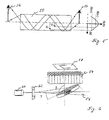
- FIG. 1 shows a section through a coin 10, for example a 1 DM coin.
- a profile created by the embossing is clearly recognizable at 12.
- a coin edge can be seen at 14 and 16 respectively.
- Fig. 1 only half of the Coin 10 shown. The other is omitted for the sake of simplicity.
- a line beam is shown in a level 20 generated.
- the line projected onto the embossing surface of the coin 10 can be stationary so that when the coin moves, for example, in or out of Run over the entire embossing surface from the projected light line beyond the drawing level becomes.
- the light line is scanned. It will be the course of the light line and so that the profile of the coin along the line is determined. This course is thicker black broken line 24 can be seen. Because special measures are not are taken to improve the resolution, the strokes are in the course of Profile line relatively small. It is e.g. B. by a resolution of 132 microns. In the array 26, which can be used instead of the array 22, and a corresponding one Optics upstream, a much better resolution, for example of less than 5 ⁇ m. This resolution can also be achieved by using an array 22 with a higher pixel density. In the The optics used can be, for example, an anamorphic optics act. Corresponding is the course 28 of the profile line. This can be used for discrimination purposes naturally evaluate better than about the profile line 24 in Array 22.
- CMOS image sensors are therefore preferred used in which a physical decoupling of the photosensitive Sensor elements are present, so that direct lighting and speckles do not have an adverse effect.
- Fig. 3 the profile of a 1 DM coin is shown, namely the eagle side.
- the profile line corresponds to the profile through the diameter of the coin.
- Fig. 2 can be seen how a coin 30 typically over a chrome mask is illuminated linearly in a Scheimpflug configuration. Between the Mask 32 and a light source 34, for example an LED, is also one suitable optics 36 arranged. The light levels 38 have to extend the Embossed image area an angle greater than 10 °, preferably between 10 ° and 30 °.
- a laser light source is used, the broadest possible Use light source to minimize the speckle effect. Using this effect does not naturally occur with an LED.
- LEDs are, for example, the arrangements shown in Fig. 4 for generating a sharp line possible.
- the light from a light emitting diode 40 is transmitted via a mirror 42 or a lens 44 bundled and projected through a gap 46 onto the coin. It is also possible the light of a light emitting diode 40 only after the gap 46 with a lens 48 bundle up.
- FIG. 5 shows the schematic structure of a gradient index lens array (GRIN lens).
- the cylindrical lens 50 has a variable refractive index n R in the radial direction such that an object 52 to be imaged is imaged as a real image 54.
- the illustration is done on a scale of 1: 1.
- a GRIN lens array 54 which is parallel to the illumination plane 56 and to the image receiver plane 58.
- the one with ⁇ designated angle between the illumination plane 56 and the normal of the GRIN field 54 is 90 °.
- the coin with its embossed image is opposite that Illumination plane inclined by an angle ⁇ between 0 ° and 90 °.
- a light source 6 shows a laser 60, the laser beam of which is directed via line optics 62 an illumination level 56 is expanded.
Landscapes
- Engineering & Computer Science (AREA)
- Physics & Mathematics (AREA)
- General Physics & Mathematics (AREA)
- Artificial Intelligence (AREA)
- Computer Vision & Pattern Recognition (AREA)
- Multimedia (AREA)
- Theoretical Computer Science (AREA)
- Testing Of Coins (AREA)
- Treatment Of Fiber Materials (AREA)
- Investigating Materials By The Use Of Optical Means Adapted For Particular Applications (AREA)
Description
- Fig. 1
- zeigt schematisch eine Anordnung zur Prägebilderkennung mit unterschiedlicher Auflösung am Bildempfänger.
- Fig. 2
- zeigt eine Möglichkeit zur Erzeugung einer Lichtlinie auf dem Prägebild einer Münze.
- Fig. 3
- zeigt eine nach dem erfindungsgemäßen Verfahren aufgenommene Profillinie einer 1 DM-Münze.
- Fign. 4a bis c
- zeigen schematische Ansichten zur Erzeugung einer Beleuchtung mittels LED.
- Fig. 5
- zeigt den Aufbau einer zylindrischen GRIN-Linse.
- Fig. 6
- zeigt die Anordnung eines GRIN-Linsenfeldes zur Prägebilderkennung.
Claims (9)
- Verfahren zur Erkennung der räumlichen Konfiguration von Münzen in einem Münzautomaten mit den folgenden Schritten:eine Lichtquelle projiziert mindestens ein zweidimensionales Lichtmuster auf die Prägefläche einer zu erkennenden Münze, wobei das Lichtmuster aus Lichtlinien besteht,die Lichtquelle trifft unter einem Winkel größer als 0° und kleiner als 90° in bezug auf die Erstreckung der Prägefläche auf die Prägefläche,die Münze wird relativ zu der stationären Lichtquelle bewegt derart, daß sukzessive ein Teil oder die gesamte Prägefläche der Münze beleuchtet wird,die beleuchtete Münzfläche wird mit einer Optik auf einen Bildempfänger abgebildet,der Verlauf des Lichtmusters wird während des Vorbeibewegens der Münze an der Lichtquelle durch den Bildempfänger aufgezeichnet,die ermittelten Bilddaten werden mit vorgegebenen Bilddaten zur Erzeugung eines Echt- oder Falschsignals durch eine Daten- und Bildverarbeitung verglichen.
- Verfahren nach Anspruch 1, dadurch gekennzeichnet, daß der Verlauf des Lichtmusters durch ein Linsenfeld abgebildet wird, das im wesentlichen parallel zur Beleuchtungsebene angeordnet ist.
- Verfahren nach Anspruch 2, dadurch gekennzeichnet, daß als Linsenfeld ein 1:1 abbildendes GRIN-Linsenfeld vorgesehen ist.
- Verfahren nach einem der Ansprüche 1 bis 3, dadurch gekennzeichnet, daß das Lichtmuster mit einem Laser und einer Linienoptik erzeugt wird.
- Verfahren nach einem der Ansprüche 1 bis 3, dadurch gekennzeichnet, daß das Lichtmuster mit einer LED und einer Maske erzeugt wird.
- Verfahren nach einem der Ansprüche 1 bis 5, dadurch gekennzeichnet, daß der Bildempfänger eine Digitalkamera, einen CCD-Sensor oder einen CMOS-Sensor bzw. -Chip verwendet.
- Verfahren nach einem der Ansprüche 1 bis 7, dadurch gekennzeichnet, daß dem Bildempfänger eine abbildende Optik vorgeschaltet ist zwecks Vergrößerung des Profilbildes in bezug auf die Profilhöhe bzw. -tiefe.
- Verfahren nach Anspruch 7, dadurch gekennzeichnet daß als abbildende Optik eine anamorphotische Optik vorgeschen ist.
- Verfahren nach einem der Ansprüche 1 bis 8, dadurch gekennzeichnet, daß in der Daten- und Bildverarbeitung eine Vergrößerung der Profilhöhe bzw. Profiltiefe und/oder eine Verkleinerung der Profillänge vorgenommen wird.
Applications Claiming Priority (2)
| Application Number | Priority Date | Filing Date | Title |
|---|---|---|---|
| DE19922489 | 1999-05-15 | ||
| DE19922489A DE19922489A1 (de) | 1999-05-15 | 1999-05-15 | Verfahren zur Erkennung der räumlichen Konfiguration von Münzen |
Publications (3)
| Publication Number | Publication Date |
|---|---|
| EP1054361A2 EP1054361A2 (de) | 2000-11-22 |
| EP1054361A3 EP1054361A3 (de) | 2001-10-31 |
| EP1054361B1 true EP1054361B1 (de) | 2003-12-03 |
Family
ID=7908224
Family Applications (1)
| Application Number | Title | Priority Date | Filing Date |
|---|---|---|---|
| EP00110169A Expired - Lifetime EP1054361B1 (de) | 1999-05-15 | 2000-05-15 | Verfahren und Vorrichtung zur Erkennung der räumlichen Konfiguration von Münzen |
Country Status (4)
| Country | Link |
|---|---|
| EP (1) | EP1054361B1 (de) |
| AT (1) | ATE255751T1 (de) |
| DE (2) | DE19922489A1 (de) |
| ES (1) | ES2208179T3 (de) |
Families Citing this family (4)
| Publication number | Priority date | Publication date | Assignee | Title |
|---|---|---|---|---|
| DE20114010U1 (de) | 2001-08-24 | 2001-10-25 | A-S Witkowski GmbH, 45899 Gelsenkirchen | Selbstbedienungsautomat und Münzprüfer |
| DE10202383A1 (de) * | 2002-01-16 | 2003-08-14 | Nat Rejectors Gmbh | Verfahren zur Erkennung eines Prägebildes einer Münze in einem Münzautomaten |
| DE10248972B4 (de) * | 2002-10-17 | 2009-09-10 | Walter Hanke Mechanische Werkstätten GmbH & Co. KG | Verfahren zum Prüfen von Münzen und münzähnlichen Gegenständen sowie ein Münzprüfer hierfür |
| AT514749A1 (de) * | 2013-09-09 | 2015-03-15 | Economa Automatisierungstechnik Gmbh | Verfahren zum Prüfen der Oberfläche von Gegenständen und Münze mit Echtheitsmerkmal |
Family Cites Families (16)
| Publication number | Priority date | Publication date | Assignee | Title |
|---|---|---|---|---|
| DE2306187A1 (de) * | 1973-02-08 | 1974-08-15 | Josef Mergili | Optoelekttonischer muenzpruefer |
| CH604288A5 (de) * | 1977-02-11 | 1978-09-15 | Landis & Gyr Ag | |
| DE2919446A1 (de) * | 1979-05-15 | 1980-11-27 | Bat Cigarettenfab Gmbh | Optisches pruefverfahren fuer gegenstaende und vorrichtung zur durchfuehrung des verfahrens |
| GB2173624B (en) | 1985-04-08 | 1988-12-14 | Qonaar Corp | Low power coin discrimination apparatus |
| DE3526378A1 (de) | 1985-07-24 | 1987-02-05 | Andras Dipl Ing Gati | Vorrichtung mit einem sensor zur erkennung von muenzen |
| NO168615C (no) * | 1989-10-17 | 1992-03-11 | Datalab Oy | Fremgangsmaate og anordning for gjenkjenning av en mynt |
| DD296769A5 (de) | 1990-07-18 | 1991-12-12 | Act Gesellschaft Fuer Soft- Und Hardwaresysteme Mbh,De | Anordnung zur pruefung der physikalischen eigenschaften von muenzen |
| JP2742360B2 (ja) * | 1992-11-13 | 1998-04-22 | ローレルバンクマシン株式会社 | 貨幣パターン検出装置 |
| JPH06208613A (ja) * | 1992-11-13 | 1994-07-26 | Laurel Bank Mach Co Ltd | パターン検出装置 |
| JP2745102B2 (ja) * | 1992-12-02 | 1998-04-28 | ローレルバンクマシン株式会社 | 硬貨判別装置 |
| JP3359158B2 (ja) * | 1994-09-14 | 2002-12-24 | 日本電産コパル株式会社 | 表面パターン読取装置 |
| JPH0997363A (ja) * | 1995-10-02 | 1997-04-08 | Oki Electric Ind Co Ltd | 硬貨撮像装置 |
| JP3516825B2 (ja) * | 1996-03-29 | 2004-04-05 | ローレルバンクマシン株式会社 | 硬貨判別装置 |
| GB9610603D0 (en) | 1996-05-21 | 1996-07-31 | Panzeri Ezio | Coin recognition apparatus |
| JPH10222716A (ja) * | 1997-02-04 | 1998-08-21 | Sankyo Seiki Mfg Co Ltd | コイン認識装置 |
| JPH1114557A (ja) * | 1997-06-25 | 1999-01-22 | Oki Electric Ind Co Ltd | 硬貨認識装置 |
-
1999
- 1999-05-15 DE DE19922489A patent/DE19922489A1/de not_active Withdrawn
-
2000
- 2000-05-15 DE DE50004617T patent/DE50004617D1/de not_active Expired - Lifetime
- 2000-05-15 ES ES00110169T patent/ES2208179T3/es not_active Expired - Lifetime
- 2000-05-15 EP EP00110169A patent/EP1054361B1/de not_active Expired - Lifetime
- 2000-05-15 AT AT00110169T patent/ATE255751T1/de not_active IP Right Cessation
Also Published As
| Publication number | Publication date |
|---|---|
| DE19922489A1 (de) | 2000-11-23 |
| ATE255751T1 (de) | 2003-12-15 |
| EP1054361A2 (de) | 2000-11-22 |
| ES2208179T3 (es) | 2004-06-16 |
| DE50004617D1 (de) | 2004-01-15 |
| EP1054361A3 (de) | 2001-10-31 |
Similar Documents
| Publication | Publication Date | Title |
|---|---|---|
| DE3822303C2 (de) | ||
| DE4338780C2 (de) | Mustererkennungsvorrichtung | |
| EP0979795B1 (de) | Verfahren zur Erkennung von Fadenresten auf Spinnkopshülsen | |
| DE3926349C2 (de) | ||
| DE10237477B4 (de) | Vorrichtung zur Messung von Oberflächendefekten | |
| EP3787900B1 (de) | Verfahren zum überprüfen eines druckzylinders und eine entsprechende anordnung | |
| DE102009058215B4 (de) | Verfahren und Vorrichtung zur Oberflächenprüfung eines Lagerbauteils | |
| DE102004047928B4 (de) | Optisches 3D-Messverfahren und Messeinrichtung | |
| EP0615607A1 (de) | Optischer abstandssensor. | |
| DE19537376A1 (de) | Autofokussierungsmikroskop | |
| DE112006001820T5 (de) | Optimieren der Verwendung und Leistung von optischen Systemen, die mit telezentrischer Dunkelfeldbeleuchtung auf der Achse implementiert werden | |
| WO1994022104A1 (de) | Verfahren zur aufnahme von strichcodierungen | |
| DE102014203645B4 (de) | Verfahren und Vorrichtung zum optischen Bestimmen eines Abstandes | |
| DE112017001937T5 (de) | Probenform-Messverfahren und Probenform-Messvorrichtung | |
| EP1634035A2 (de) | Interferometrische messvorrichtung | |
| EP1054361A2 (de) | Verfahren und Vorrichtung zur Erkennung der räumlichen Konfiguration von Münzen | |
| EP3267367B1 (de) | Zählscheibenvorrichtung | |
| DE10244767A1 (de) | Verfahren und Vorrichtung zum Bestimmen des Abstands zwischen einer Referenzebene und einer inneren oder äußeren optischen Grenzfläche eines Objekts sowie Verwendung derselben zum Bestimmen eines Oberflächenprofils eines, inbesondere metallischen, Objekts, Autofokus-Modul, Mikroskop und Verfahren zum Autofokussieren eines Mikroskops | |
| DE10139717A1 (de) | Verfahren und Vorrichtung zur Untersuchung von Defekten in oder auf Blattgut | |
| EP1563467B1 (de) | Verfahren zur fotografischen aufnahme eines zylinderförmigen, insbesondere plattenförmigen gegenstandes | |
| DE112009001936B4 (de) | Inspektionsvorrichtung- und Verfahren für die optische Untersuchung von Objektoberflächen, insbesondere von Waferkanten | |
| DE10063786A1 (de) | Vorrichtung und Verfahren zum Vermessen eines Gegenstandes | |
| EP1197926A2 (de) | Verfahren zur Erkennung eines Prägebilds einer Münze in einem Münzautomaten | |
| EP2565851A2 (de) | Vorrichtung zur Rücknahme von Leergut und Verfahren zum Klassifizieren von Leergut mit Hilfe von Lichtfeldern | |
| DE10028201A1 (de) | Verfahren und Vorrichtung zum optischen Prüfen von Oberflächen bewegter Gegenstände |
Legal Events
| Date | Code | Title | Description |
|---|---|---|---|
| PUAI | Public reference made under article 153(3) epc to a published international application that has entered the european phase |
Free format text: ORIGINAL CODE: 0009012 |
|
| AK | Designated contracting states |
Kind code of ref document: A2 Designated state(s): AT BE CH CY DE DK ES FI FR GB GR IE IT LI LU MC NL PT SE |
|
| AX | Request for extension of the european patent |
Free format text: AL;LT;LV;MK;RO;SI |
|
| RIN1 | Information on inventor provided before grant (corrected) |
Inventor name: MEYER, WILFRIED Inventor name: EICH, MANFRED PROF. DR. Inventor name: ADAMECK, MARKUS Inventor name: COHRS, ULRICH |
|
| PUAL | Search report despatched |
Free format text: ORIGINAL CODE: 0009013 |
|
| AK | Designated contracting states |
Kind code of ref document: A3 Designated state(s): AT BE CH CY DE DK ES FI FR GB GR IE IT LI LU MC NL PT SE |
|
| AX | Request for extension of the european patent |
Free format text: AL;LT;LV;MK;RO;SI |
|
| 17P | Request for examination filed |
Effective date: 20020213 |
|
| 17Q | First examination report despatched |
Effective date: 20020515 |
|
| AKX | Designation fees paid |
Free format text: AT BE CH CY DE DK ES FI FR GB GR IE IT LI LU MC NL PT SE |
|
| GRAH | Despatch of communication of intention to grant a patent |
Free format text: ORIGINAL CODE: EPIDOS IGRA |
|
| GRAS | Grant fee paid |
Free format text: ORIGINAL CODE: EPIDOSNIGR3 |
|
| GRAA | (expected) grant |
Free format text: ORIGINAL CODE: 0009210 |
|
| AK | Designated contracting states |
Kind code of ref document: B1 Designated state(s): AT BE CH CY DE DK ES FI FR GB GR IE IT LI LU MC NL PT SE |
|
| PG25 | Lapsed in a contracting state [announced via postgrant information from national office to epo] |
Ref country code: FI Free format text: LAPSE BECAUSE OF FAILURE TO SUBMIT A TRANSLATION OF THE DESCRIPTION OR TO PAY THE FEE WITHIN THE PRESCRIBED TIME-LIMIT Effective date: 20031203 Ref country code: IE Free format text: LAPSE BECAUSE OF FAILURE TO SUBMIT A TRANSLATION OF THE DESCRIPTION OR TO PAY THE FEE WITHIN THE PRESCRIBED TIME-LIMIT Effective date: 20031203 Ref country code: CY Free format text: LAPSE BECAUSE OF FAILURE TO SUBMIT A TRANSLATION OF THE DESCRIPTION OR TO PAY THE FEE WITHIN THE PRESCRIBED TIME-LIMIT Effective date: 20031203 |
|
| REG | Reference to a national code |
Ref country code: GB Ref legal event code: FG4D Free format text: NOT ENGLISH |
|
| RIN1 | Information on inventor provided before grant (corrected) |
Inventor name: COHRS, ULRICH Inventor name: MEYER, WILFRIED Inventor name: ADAMECK, MARKUS Inventor name: EICH, MANFRED PROF. DR. |
|
| REG | Reference to a national code |
Ref country code: CH Ref legal event code: NV Representative=s name: ING. MARCO ZARDI C/O M. ZARDI & CO. S.A. Ref country code: CH Ref legal event code: EP |
|
| REG | Reference to a national code |
Ref country code: IE Ref legal event code: FG4D Free format text: GERMAN |
|
| REF | Corresponds to: |
Ref document number: 50004617 Country of ref document: DE Date of ref document: 20040115 Kind code of ref document: P |
|
| PG25 | Lapsed in a contracting state [announced via postgrant information from national office to epo] |
Ref country code: SE Free format text: LAPSE BECAUSE OF FAILURE TO SUBMIT A TRANSLATION OF THE DESCRIPTION OR TO PAY THE FEE WITHIN THE PRESCRIBED TIME-LIMIT Effective date: 20040303 Ref country code: GR Free format text: LAPSE BECAUSE OF FAILURE TO SUBMIT A TRANSLATION OF THE DESCRIPTION OR TO PAY THE FEE WITHIN THE PRESCRIBED TIME-LIMIT Effective date: 20040303 Ref country code: DK Free format text: LAPSE BECAUSE OF FAILURE TO SUBMIT A TRANSLATION OF THE DESCRIPTION OR TO PAY THE FEE WITHIN THE PRESCRIBED TIME-LIMIT Effective date: 20040303 |
|
| GBT | Gb: translation of ep patent filed (gb section 77(6)(a)/1977) |
Effective date: 20040220 |
|
| PG25 | Lapsed in a contracting state [announced via postgrant information from national office to epo] |
Ref country code: AT Free format text: LAPSE BECAUSE OF NON-PAYMENT OF DUE FEES Effective date: 20040515 |
|
| PG25 | Lapsed in a contracting state [announced via postgrant information from national office to epo] |
Ref country code: MC Free format text: LAPSE BECAUSE OF NON-PAYMENT OF DUE FEES Effective date: 20040531 |
|
| REG | Reference to a national code |
Ref country code: ES Ref legal event code: FG2A Ref document number: 2208179 Country of ref document: ES Kind code of ref document: T3 |
|
| REG | Reference to a national code |
Ref country code: IE Ref legal event code: FD4D |
|
| ET | Fr: translation filed | ||
| PLBE | No opposition filed within time limit |
Free format text: ORIGINAL CODE: 0009261 |
|
| STAA | Information on the status of an ep patent application or granted ep patent |
Free format text: STATUS: NO OPPOSITION FILED WITHIN TIME LIMIT |
|
| 26N | No opposition filed |
Effective date: 20040906 |
|
| REG | Reference to a national code |
Ref country code: CH Ref legal event code: PCAR Free format text: ISLER & PEDRAZZINI AG;POSTFACH 1772;8027 ZUERICH (CH) |
|
| PG25 | Lapsed in a contracting state [announced via postgrant information from national office to epo] |
Ref country code: PT Free format text: LAPSE BECAUSE OF NON-PAYMENT OF DUE FEES Effective date: 20040503 |
|
| PGFP | Annual fee paid to national office [announced via postgrant information from national office to epo] |
Ref country code: ES Payment date: 20080306 Year of fee payment: 9 |
|
| PGFP | Annual fee paid to national office [announced via postgrant information from national office to epo] |
Ref country code: CH Payment date: 20080530 Year of fee payment: 9 Ref country code: FR Payment date: 20080228 Year of fee payment: 9 Ref country code: LU Payment date: 20080425 Year of fee payment: 9 |
|
| PGFP | Annual fee paid to national office [announced via postgrant information from national office to epo] |
Ref country code: BE Payment date: 20080225 Year of fee payment: 9 |
|
| PGFP | Annual fee paid to national office [announced via postgrant information from national office to epo] |
Ref country code: IT Payment date: 20080522 Year of fee payment: 9 |
|
| PGFP | Annual fee paid to national office [announced via postgrant information from national office to epo] |
Ref country code: NL Payment date: 20080531 Year of fee payment: 9 |
|
| PGFP | Annual fee paid to national office [announced via postgrant information from national office to epo] |
Ref country code: GB Payment date: 20080521 Year of fee payment: 9 |
|
| BERE | Be: lapsed |
Owner name: *NATIONAL REJECTORS INC. G.M.B.H. Effective date: 20090531 |
|
| REG | Reference to a national code |
Ref country code: CH Ref legal event code: PL |
|
| GBPC | Gb: european patent ceased through non-payment of renewal fee |
Effective date: 20090515 |
|
| PG25 | Lapsed in a contracting state [announced via postgrant information from national office to epo] |
Ref country code: LI Free format text: LAPSE BECAUSE OF NON-PAYMENT OF DUE FEES Effective date: 20090531 Ref country code: CH Free format text: LAPSE BECAUSE OF NON-PAYMENT OF DUE FEES Effective date: 20090531 |
|
| NLV4 | Nl: lapsed or anulled due to non-payment of the annual fee |
Effective date: 20091201 |
|
| PG25 | Lapsed in a contracting state [announced via postgrant information from national office to epo] |
Ref country code: NL Free format text: LAPSE BECAUSE OF NON-PAYMENT OF DUE FEES Effective date: 20091201 |
|
| REG | Reference to a national code |
Ref country code: FR Ref legal event code: ST Effective date: 20100129 |
|
| PG25 | Lapsed in a contracting state [announced via postgrant information from national office to epo] |
Ref country code: FR Free format text: LAPSE BECAUSE OF NON-PAYMENT OF DUE FEES Effective date: 20090602 |
|
| PG25 | Lapsed in a contracting state [announced via postgrant information from national office to epo] |
Ref country code: GB Free format text: LAPSE BECAUSE OF NON-PAYMENT OF DUE FEES Effective date: 20090515 |
|
| PG25 | Lapsed in a contracting state [announced via postgrant information from national office to epo] |
Ref country code: BE Free format text: LAPSE BECAUSE OF NON-PAYMENT OF DUE FEES Effective date: 20090531 |
|
| REG | Reference to a national code |
Ref country code: ES Ref legal event code: FD2A Effective date: 20090516 |
|
| PG25 | Lapsed in a contracting state [announced via postgrant information from national office to epo] |
Ref country code: ES Free format text: LAPSE BECAUSE OF NON-PAYMENT OF DUE FEES Effective date: 20090516 |
|
| PG25 | Lapsed in a contracting state [announced via postgrant information from national office to epo] |
Ref country code: IT Free format text: LAPSE BECAUSE OF NON-PAYMENT OF DUE FEES Effective date: 20090515 |
|
| PG25 | Lapsed in a contracting state [announced via postgrant information from national office to epo] |
Ref country code: LU Free format text: LAPSE BECAUSE OF NON-PAYMENT OF DUE FEES Effective date: 20090515 |
|
| PGFP | Annual fee paid to national office [announced via postgrant information from national office to epo] |
Ref country code: DE Payment date: 20110709 Year of fee payment: 12 |
|
| REG | Reference to a national code |
Ref country code: DE Ref legal event code: R119 Ref document number: 50004617 Country of ref document: DE Effective date: 20121201 |
|
| PG25 | Lapsed in a contracting state [announced via postgrant information from national office to epo] |
Ref country code: DE Free format text: LAPSE BECAUSE OF NON-PAYMENT OF DUE FEES Effective date: 20121201 |