EP1041441A2 - Verfahren zur Herstellung einer Anordnung - Google Patents
Verfahren zur Herstellung einer Anordnung Download PDFInfo
- Publication number
- EP1041441A2 EP1041441A2 EP00302535A EP00302535A EP1041441A2 EP 1041441 A2 EP1041441 A2 EP 1041441A2 EP 00302535 A EP00302535 A EP 00302535A EP 00302535 A EP00302535 A EP 00302535A EP 1041441 A2 EP1041441 A2 EP 1041441A2
- Authority
- EP
- European Patent Office
- Prior art keywords
- mask
- exposure
- layer
- pattern
- fine
- Prior art date
- Legal status (The legal status is an assumption and is not a legal conclusion. Google has not performed a legal analysis and makes no representation as to the accuracy of the status listed.)
- Withdrawn
Links
Images


Classifications
-
- G—PHYSICS
- G03—PHOTOGRAPHY; CINEMATOGRAPHY; ANALOGOUS TECHNIQUES USING WAVES OTHER THAN OPTICAL WAVES; ELECTROGRAPHY; HOLOGRAPHY
- G03F—PHOTOMECHANICAL PRODUCTION OF TEXTURED OR PATTERNED SURFACES, e.g. FOR PRINTING, FOR PROCESSING OF SEMICONDUCTOR DEVICES; MATERIALS THEREFOR; ORIGINALS THEREFOR; APPARATUS SPECIALLY ADAPTED THEREFOR
- G03F7/00—Photomechanical, e.g. photolithographic, production of textured or patterned surfaces, e.g. printing surfaces; Materials therefor, e.g. comprising photoresists; Apparatus specially adapted therefor
- G03F7/70—Microphotolithographic exposure; Apparatus therefor
- G03F7/70425—Imaging strategies, e.g. for increasing throughput or resolution, printing product fields larger than the image field or compensating lithography- or non-lithography errors, e.g. proximity correction, mix-and-match, stitching or double patterning
- G03F7/70466—Multiple exposures, e.g. combination of fine and coarse exposures, double patterning or multiple exposures for printing a single feature
-
- H10P76/00—
-
- G—PHYSICS
- G03—PHOTOGRAPHY; CINEMATOGRAPHY; ANALOGOUS TECHNIQUES USING WAVES OTHER THAN OPTICAL WAVES; ELECTROGRAPHY; HOLOGRAPHY
- G03F—PHOTOMECHANICAL PRODUCTION OF TEXTURED OR PATTERNED SURFACES, e.g. FOR PRINTING, FOR PROCESSING OF SEMICONDUCTOR DEVICES; MATERIALS THEREFOR; ORIGINALS THEREFOR; APPARATUS SPECIALLY ADAPTED THEREFOR
- G03F7/00—Photomechanical, e.g. photolithographic, production of textured or patterned surfaces, e.g. printing surfaces; Materials therefor, e.g. comprising photoresists; Apparatus specially adapted therefor
- G03F7/20—Exposure; Apparatus therefor
- G03F7/2022—Multi-step exposure, e.g. hybrid; backside exposure; blanket exposure, e.g. for image reversal; edge exposure, e.g. for edge bead removal; corrective exposure
Definitions
- This invention relates to a device manufacturing method usable for manufacture of various electronic devices such as semiconductor chips (e.g., IC or LSI), display device (e.g., liquid crystal panel), detecting device (e.g., magnetic head) or image pickup device (e.g., CCD), for example.
- semiconductor chips e.g., IC or LSI
- display device e.g., liquid crystal panel
- detecting device e.g., magnetic head
- image pickup device e.g., CCD
- a mask or reticle (original) is therefore formed with a pattern of a size magnified by 4x or 5x as compared with a pattern to be produced on a semiconductor wafer (substrate to be exposed).
- an X-ray mask (original) is formed with a pattern of the same size as a pattern to be produced on a substrate.
- the controllability of electric voltage to be applied to a deflector is influential to the pattern position control. Further, depending on the flatness (irregularity) of a workpiece to be patterned, a pattern position distortion occurs.
- an X-ray proximity exposure process in addition to the positional distortion of an original itself produced by an electron beam patterning apparatus, there occurs a distortion of an X-ray mask. That is, usually, in an X-ray mask, a pattern of X-ray absorptive material of a thickness of about 0.4 micron is formed on an X-ray transmissive film of a thickness of about 2 microns, for example. Due to a stress distribution of the transmissive film or to a stress of the absorptive material, a positional distortion occurs. Further, during the X-ray proximity exposure process, since the X-ray beam is not a completely parallel beam, there occurs a distortion, called a runout error.
- Japanese Patent Application, Application No. H9-304232 filed by the same assignee of the subject application, proposes an exposure method which assures pattern formation of higher resolution and higher positional precision, as compared with those attainable currently, by use of a mask that can be produced by current techniques and an exposure apparatus currently available.
- this exposure method a fine pattern exposure and a rough pattern exposure are performed superposedly (by dual or multiple exposure) upon a layer on a substrate, to thereby assure enhancement of resolution. This method will be briefly explained below.
- the fine pattern exposure is an exposure process for a pattern having a periodic structure.
- a rough pattern having a desired pattern corresponding to those portions to be left is printed by dual or multiple exposures.
- a development process is performed thereto, under a condition by which the fine pattern at those portion (positions) having been exposed to the rough pattern remains.
- the fine pattern exposure amount and the rough pattern exposure amount are determined at a ratio by which a best resist pattern it obtainable.
- a device manufacturing method including a process for exposure of a first layer on a substrate and a process for exposure of a second layer on the substrate, wherein each exposure of the first and second layers is performed by use of a plurality of originals, and wherein at least one of the originals to be used for exposure of the first layer has the same design rule as that of at least one of the originals to be used for exposure of the second layer.
- the masks having the same design rule may be an identical mask to be used for exposures of both the first and second layers.
- At least a portion of the first or second layer may be exposed by use of at least one of an X-ray, an ultraviolet ray, an extreme ultraviolet ray, and an electron beam.
- Each of the first and second layers may be exposed superposedly by use of a fine pattern original having a relatively fine pattern and a rough pattern original having a relatively rough pattern.
- Each fine pattern to be printed on the first and second layers may have a periodic structure.
- Each rough pattern to be printed on the first and second layers may comprise different patterns.
- At least one pattern for each layer includes a portion having a common design rule.
- the pattern registration precision between different layers can be improved significantly.
- a pattern can be produced at higher resolution and precision, with a good registration precision between different layers.
- At least two originals may be used, including, for example, a first original for printing a fine pattern having a relatively small minimum linewidth upon a layer on a substrate and a second original for printing a rough pattern, formed with a target precision corresponding to a minimum linewidth larger than that of the fine pattern.
- first layer referred to in this specification is not limited to a layer first provided on a bare wafer. It may include an initial layer of two or more layers to be provided superposedly.
- second layer refers to a layer which is superposedly provided after formation of a "first layer”. Further, it is not always necessary that a "first layer” and a “second layer” are formed successively. Namely, after a certain layer is formed subsequent to formation of a "first layer”, a "second layer” may be formed superposedly on the "first layer”.
- a relatively fine pattern and a relatively rough pattern are superposedly photoprinted upon different layers on a substrate such as a semiconductor wafer or a glass plate.
- a resist material on the substrate for the first layer is exposed by dual exposure, comprising a fine pattern exposure and a rough pattern exposure, by which a resist pattern as required for the first layer is transferred to the substrate.
- the position of the resist pattern to be resolved here is strongly dependent upon the position of the fine pattern image as transferred. This is because a latent image as formed on the resist corresponds to the superposition of a fine pattern image and a rough pattern image, and such portion of the latent image as having an exposure intensity higher than a certain threshold remains there as a resist pattern.
- a second layer to be formed on the substrate is also produced by dual exposure, comprising a fine pattern exposure and a rough pattern exposure.
- the resist pattern of the second layer is strongly dependent upon the position of the fine pattern used in the exposure of the second layer.
- a fine mask to be used for formation of a fine pattern of a second layer may be a mask having a portion of the same design as that of a mask having been used for formation of a fine pattern image of a first layer. Alternatively, it may be the same mask as has been used for formation of the fine pattern image of the first layer. By using such mask, a fine pattern image of the second layer is printed.
- a second original for rough pattern exposure may be one which differs from a first original for fine pattern exposure in respect to the type of an absorptive material or the thickness thereof. They may be determined to satisfy a condition for attaining a desired rough pattern.
- an exposure region may be divided in accordance with a fine pattern, and a range of divided zones may be selected in accordance with a rough pattern.
- a resist pattern after development is strongly dependent upon the precision of the fine pattern.
- the invention is applied to a device manufacture wherein a channel-shaped gate electrode layer of polysilicon (first layer) is formed through a proximity X-ray exposure and wherein a wiring contact hole (second layer) is formed.
- first layer a channel-shaped gate electrode layer of polysilicon
- second layer a wiring contact hole
- the first layer formation will be described in regard to a fine pattern exposure for a first layer and a rough pattern exposure for the first layer, separately.
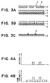
- Figure 1A shows a fine mask 4 wherein a fine pattern 1 of periodic structure is formed at a central portion (exposure picture angle) while alignment marks 2 are formed around it.
- a fine pattern 1 of periodic structure As regards the structure of the fine pattern 1, it comprises a periodic pattern defined by lines and spaces.
- the section of the fine mask 4 has a structure such as shown in Figure 1C.
- the fine pattern 1 comprises an absorptive material such as W (tungsten) for absorbing X-rays, and a mask membrane 3 such as SiC for supporting it.
- Figure 1B shows a wafer 8 which is a substrate to be exposed.
- a positive type resist material is applied to the surface thereof to be exposed.
- FIG 3A there is a SiO 2 layer 7 already formed on the wafer 8.
- an alignment operation is performed for alignment between the alignment marks 2 and 9 of the fine mask 4 and the wafer 8, and then X-rays are projected from the above of the mask 4.
- the X-rays are blocked by those areas where an X-ray absorptive material is present and, as shown in Figure 1B, X-rays passing through the remaining areas are absorbed by the resist, whereby a latent image (invisible image) 1' of the fine pattern 1 is formed there.
- the intensity distributions at each section A-A in Figures 1A and 1B are such as shown in Figure 1C.
- Figure 1C shows an exposure amount distribution and a fine pattern corresponding to it.
- a rough pattern exposure is performed without intervention of a development process.
- Figure 2 shows a rough mask 12 having a rough pattern 5 which is formed with a desired shape, at its central portion thereof. There are alignment marks 2 around the mask.
- Figure 3A is a sectional view corresponding to a section A'-A' in Figure 2 in an exposure process.
- the rough mask 12 has a rough pattern 5 made of an X-ray absorptive material such as W (tungsten), and a mask membrane 13.
- W tungsten
- Figure 4A shows an intensity distribution upon the mask, as produced by this exposure process.
- the intensity distribution provided by the rough pattern as shown in Figure 4A is accumulated on the intensity distribution ( Figure 1C) of the fine pattern already formed as a latent image, such that a combined intensity distribution ( Figure 4B), i.e., an exposure amount distribution, is produced as a latent image of the first layer.
- the alignment marks 9 of the wafer 8 are to be used again in exposure of a second layer. For this reason, during the fine pattern exposure and the rough pattern exposure, an X-ray blocking plate (masking blade) is used to prevent exposure of these alignment marks 9 with X-rays.
- the exposure process described above uses a positive type resist.
- the resist material in a portion exposed with a large exposure amount is solved and removed.
- the resist can be solved into the shape of the rough pattern 5 as shown in Figure 3B, such that the SiO 2 layer 7 can be uncovered.
- a polysilicon layer is formed by a lift-off method and, thereafter, the resist is peeled, whereby a structure such as shown in Figure 3C is produced.
- a second rough mask may be used to enlarge the exposure amount only in that portion.
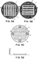
- Figure 5A show the same fine mask 4 having been used for the first layer (Figure 1A).
- Figure 5B shows a fine mask 13 having a fine pattern 11 extending orthogonally to that of Figure 5A. Like the fine mask 4 of Figure 5A, it is formed with alignment mark 2 around the same.
- Figure 5C shows a wafer 8 to be exposed, and it has a surface being coated with a negative type resist material. The first layer process has already been done, to this wafer.
- an SiO 2 layer 15 (insulating layer) is formed over the whole wafer surface ( Figure 7A). Since the alignment marks 9 are not damaged during formation of the first layer, the same alignment marks 9 can be used for exposure of the second layer.
- the mask 4 of Figure 5A is used, and an alignment operation is performed for alignment between the alignment marks 2 and 9 of the fine mask 4 and the wafer 8, and then X-rays are projected from the above of the mask 4.
- X-rays pass through those areas without a mask absorptive material, such that a latent image 1' (invisible image) of the fine pattern 1 is produced on the resist of the wafer 8.
- the mask 13 of Figure 5B is used, and an alignment operation is performed for alignment between the alignment marks 2 and 9 of the fine mask 13 and the wafer, and then X-rays are projected from the above of the mask 13.
- a latent image 11' of the fine pattern 11 is produced.
- Figure 5D shows the result. More specifically, Figure 5D shows an exposure intensity distribution, corresponding to sections each along a line B-B in Figures 5A, 5B and 5C. The position on the wafer 8 surface is taken on the axis of abscissa, while the total exposure intensity is taken on the axis of ordinate.
- Figure 6 shows a rough mask 12' for a second layer.
- absorptive material 20 at a region within the picture angle, where a contact hole is to be formed.
- Alignment marks 2 are formed outside the picture angle.
- Figure 7A shows the section along a line B'-B' in Figure 6 in the exposure process.
- the exposure intensity distribution as obtainable with the rough mask 12' only is such as shown in Figure 8A.
- FIG. 8A Those portions with lower exposure intensity shown in Figure 8A are the areas where contact holes are to be produced, and they correspond to the absorptive material positions on the mask 12'. These positions just correspond to the low exposure intensity positions of the fine mask.
- an exposure intensity distribution as provided by combining the exposure intensity distribution (Figure 5D) through the fine mask exposure and the exposure intensity distribution (Figure 8A) through the rough mask exposure will be such as shown in Figure 8D.
- the intensity at the position where a contact hole is to be formed is lowest.
- a resist pattern 14 defined after a development process is such as shown in Figure 7B.
- the insulating layers 15 and 7 are etched, and contact holes are produced.
- the masks of Figures 1A and 5A are identical (one and the same mask)
- the mask alignment marks 2 are brought into alignment with respect to wafer alignment marks 9 having been formed on a layer before exposure of the first layer. With this procedure, exact alignment can be accomplished.
- the masks 4 and 12 may be brought into alignment beforehand, with respect to alignment marks provided on a reference table of an exposure apparatus, such that the alignment of the masks 4 and 12 can be assured. Then, each mask is placed at the exposure position, and the exposure process is performed.
- alignment marks 2 there are two types of marks, that is, an alignment mark for producing an alignment mark upon a wafer, and an alignment mark for aligning a mask with respect to an alignment mark formed on a wafer.
- an alignment mark for producing an alignment mark upon a wafer
- an alignment mark for aligning a mask with respect to an alignment mark formed on a wafer.
- a mask alignment mark is aligned with respect to an alignment mark formed through exposure of the first layer, to accomplish the mask-to-wafer alignment.
- the alignment method for the first and second layers described above is applicable not only to a case wherein the first layer is a layer to be produced on a bare wafer first.
- alignment marks for producing alignment marks on a wafer, as well as alignment marks for aligning a mask with alignment marks formed on the wafer can be provided in juxtaposition with each other, and the positional relation of them can be set very precisely. Therefore, two layers can be aligned and registered with higher precision.
- the positions of the rough pattern 5 of the first layer and the rough pattern 5' of the second layer both strongly depend on the position of the fine pattern 1 of the common mask 4.
- both of these layers are aligned with respect to the alignment marks 9 on the same wafer 8, the alignment error becomes very small. For this reason, even if the position of the fine pattern 1 of the mask 4 is deviated from a predetermined position, the positions of the rough patterns of the first and second layers also shift as the same as the deviation, and thus the registration precision between these layers increases.
- a common mask 4 is used for both layers, it is not always necessary that one and the same fine pattern is used for plural layers. Different masks may be used, provided that the same structure (design rule) is defined in at least a portion of the fine patterns, where high precision registration is required.
- Figure 9A shows a fine mask 4 (first mask) for a first layer, and it has a fine pattern 1 of periodic structure formed at a central portion (picture angle) of the mask. There are alignment marks 2 formed outside the picture angle.
- Figure 9B shows a rough mask 12 (second mask) for the first layer, and it has a rough pattern 5 formed at a central portion (picture angle) of the mask. There are alignment marks 2 formed outside the picture angle.
- an intensity distribution of a fine pattern image, of a period a half of the period of the fine pattern 1, is produced. This can be accomplished by controlling the spacing between the mask 1 and a wafer so that the same X-ray intensity is provided at the center of an absorptive material of the fine pattern and at the center of the opening.
- the rough pattern 5 inside the picture angle of the rough mask 12 for the first layer consists of a relatively fine pattern formed over the whole surface thereof.
- a dual or multiple exposure with the fine pattern 1 is preferable since then the resolution increases within the whole picture angle.
- the fine pattern 1 of the mask 4 is therefore formed throughout the picture angle region.
- An intensity distribution to be produced by a dual or multiple exposure of the fine mask 4 and the rough mask 2 will be such as shown in Figure 9C.
- Figure 10A shows a fine mask 4' for a first layer, and it has a fine pattern 1' of a predetermined periodic structure formed at a central portion (picture angle) of the mask. There are alignment marks 2 formed outside the picture angle.
- Figure 10B shows a rough mask 12' for the first layer, and it has rough patterns 5' and 5'' formed within the picture angle of the mask. There are alignment marks 2 formed outside the picture angle.
- the rough pattern in the picture angle of the rough mask 12' for the second layer includes a relatively-fine rough pattern 5' at the center of the picture angle, and a relatively-large rough pattern 5'' at a peripheral portion thereof.
- a relatively-fine rough pattern 5' at the center of the picture angle
- a relatively-large rough pattern 5'' at a peripheral portion thereof.
- a fine mask 12' having a fine pattern 1' only in the region corresponding to the region of the relatively-fine rough pattern 5' and having no such fine pattern 1' in the region corresponding to the relatively-large rough pattern 5'' in the peripheral portion (so that an ordinary exposure is carried out), is used for fine pattern exposure of the second layer.
- An intensity distribution to be produced by a dual or multiple exposure of the fine mask 4' and the rough mask 12' will be such as shown in Figure 10C.
- the fine mask 4 for the first layer and the fine mask 4' for the second layer have fine patterns of the same design rule. Also, the fine patterns of these layers to be produced are dependent upon the position of the fine pattern. Therefore, the registration precision between these fine patterns increases.
- a large rough pattern 5'' at the peripheral portion of the picture angle and a relatively-fine rough pattern 5' at the central portion of the picture angle may be printed by multiple exposure, using separate rough masks.
- the fine mask 4' used for exposure of the layer 2 does not have a fine pattern 1' in it peripheral region where the large pattern is present. It is a possible alternative that the same fine mask 4' is used for exposures of two layers while, in the exposure of the second layer with the fine pattern 1, the peripheral portion of the picture angle of the fine mask 4 is covered by a blocking plate, so that the fine pattern exposure is performed while preventing the peripheral portion being irradiated with X-rays. In that occasion, since no fine pattern is transferred to the region where the large pattern 5'' of the rough mask 12' is present, the result is transfer of only the large pattern 5''. Thus, advantageous effects as those of the second example are attainable.
- the invention is applied to a proximity X-ray exposure process.
- the invention is applicable also to various exposure processes such as, for example, a DUV exposure process using extreme ultraviolet rays such as excimer laser (e.g., ArF excimer laser), an X-ray reduction projection exposure process using soft X-rays and a reflection type mask, an electron beam simultaneous exposure process wherein an electron beam is projected to a stencil mask and wherein transmitted electron beam is reduced, and an ion beam exposure process wherein an ion beam is projected in place of an electron beam.
- extreme ultraviolet rays such as excimer laser (e.g., ArF excimer laser)
- an X-ray reduction projection exposure process using soft X-rays and a reflection type mask such as, for example, a DUV exposure process using extreme ultraviolet rays such as excimer laser (e.g., ArF excimer laser), an X-ray reduction projection exposure process using soft X-rays and a reflection type mask, an electron beam simultaneous exposure process where
- a fine mask to be used in such various exposure processes may comprise a mask having an absorptive material formed into a line-and-space shape as described in the first example, or alternatively, it may be a mask using phase shift.
- a mask such as a Levenson type mask, having such structure that the phase changes periodically, may be used to form a fine pattern on a wafer.
- each layer is produced by superposition of a fine pattern and a rough pattern.
- These layers may be formed by using different exposure methods. This is because, in general, while resist materials have different sensitivities, each has a sensitivity to light rays, electrons and X-rays. Therefore, even if the same resist is irradiated by different types of beams, exposure amounts by them can be combined.
- fine patterns of plural layers may be printed by X-ray proximity exposures while the rough pattern transfer may be performed by DUV exposure.
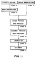
- Figure 11 is a flow chart of procedure for manufacture of microdevices such as semiconductor chips (e.g. ICs or LSIs), liquid crystal panels, CCDs, thin film magnetic heads or micro-machines, for example.
- semiconductor chips e.g. ICs or LSIs
- liquid crystal panels e.g. CCDs
- thin film magnetic heads e.g. MEMS-machines
- Step 1 is a design process for designing a circuit of a semiconductor device.
- Step 2 is a process for making a mask on the basis of the circuit pattern design.
- Step 3 is a process for preparing a wafer by using a material such as silicon.
- Step 4 is a wafer process (called a pre-process) wherein, by using the so prepared mask and wafer, circuits are practically formed on the wafer through lithography.
- Step 5 subsequent to this is an assembling step (called a post-process) wherein the wafer having been processed by step 4 is formed into semiconductor chips.
- This step includes an assembling (dicing and bonding) process and a packaging (chip sealing) process.
- Step 6 is an inspection step wherein operation check, durability check and so on for the semiconductor devices provided by step 5, are carried out. With these processes, semiconductor devices are completed and they are shipped (step 7).
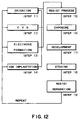
- Figure 12 is a flow chart showing details of the wafer process.
- Step 11 is an oxidation process for oxidizing the surface of a wafer.
- Step 12 is a CVD process for forming an insulating film on the wafer surface.
- Step 13 is an electrode forming process for forming electrodes upon the wafer by vapor deposition.
- Step 14 is an ion implanting process for implanting ions to the wafer.
- Step 15 is a resist process for applying a resist (photosensitive material) to the wafer.
- Step 16 is an exposure process for printing, by exposure, the circuit pattern of the mask on the wafer through the exposure apparatus described above.
- Step 17 is a developing process for developing the exposed wafer.
- Step 18 is an etching process for removing portions other than the developed resist image.
- Step 19 is a resist separation process for separating the resist material remaining on the wafer after being subjected to the etching process. By repeating these processes, circuit patterns are superposedly formed on the wafer.
Landscapes
- Physics & Mathematics (AREA)
- General Physics & Mathematics (AREA)
- Exposure And Positioning Against Photoresist Photosensitive Materials (AREA)
- Exposure Of Semiconductors, Excluding Electron Or Ion Beam Exposure (AREA)
Applications Claiming Priority (2)
| Application Number | Priority Date | Filing Date | Title |
|---|---|---|---|
| JP11085862A JP2000277427A (ja) | 1999-03-29 | 1999-03-29 | デバイス製造方法 |
| JP8586299 | 1999-03-29 |
Publications (2)
| Publication Number | Publication Date |
|---|---|
| EP1041441A2 true EP1041441A2 (de) | 2000-10-04 |
| EP1041441A3 EP1041441A3 (de) | 2003-10-01 |
Family
ID=13870708
Family Applications (1)
| Application Number | Title | Priority Date | Filing Date |
|---|---|---|---|
| EP00302535A Withdrawn EP1041441A3 (de) | 1999-03-29 | 2000-03-28 | Verfahren zur Herstellung einer Anordnung |
Country Status (4)
| Country | Link |
|---|---|
| US (1) | US6645707B2 (de) |
| EP (1) | EP1041441A3 (de) |
| JP (1) | JP2000277427A (de) |
| KR (1) | KR20010006896A (de) |
Families Citing this family (3)
| Publication number | Priority date | Publication date | Assignee | Title |
|---|---|---|---|---|
| US6856029B1 (en) * | 2001-06-22 | 2005-02-15 | Lsi Logic Corporation | Process independent alignment marks |
| US20050064346A1 (en) * | 2003-09-19 | 2005-03-24 | Matsushita Electric Industrial Co., Ltd. | Method for forming resist pattern, method for manufacturing master information carrier, magnetic recording medium, and magnetic recording/reproducing apparatus, and magnetic recording/reproducing apparatus |
| US9003338B2 (en) * | 2013-03-15 | 2015-04-07 | Taiwan Semiconductor Manufacturing Company Limited | Common template for electronic article |
Family Cites Families (11)
| Publication number | Priority date | Publication date | Assignee | Title |
|---|---|---|---|---|
| JPS58209124A (ja) * | 1982-05-31 | 1983-12-06 | Toshiba Corp | レジストパタ−ン形成方法 |
| JP2690960B2 (ja) * | 1988-09-07 | 1997-12-17 | 株式会社日立製作所 | 拡大投影露光方法及びその装置 |
| JP3163666B2 (ja) * | 1991-07-29 | 2001-05-08 | ソニー株式会社 | 位相シフトマスクを用いたパターン形成方法 |
| JPH0777796A (ja) | 1993-09-10 | 1995-03-20 | Fujitsu Ltd | 露光用マスク及び露光方法 |
| US5482819A (en) * | 1994-04-04 | 1996-01-09 | National Semiconductor Corporation | Photolithographic process for reducing repeated defects |
| US5759744A (en) * | 1995-02-24 | 1998-06-02 | University Of New Mexico | Methods and apparatus for lithography of sparse arrays of sub-micrometer features |
| JPH09236930A (ja) | 1995-12-26 | 1997-09-09 | Fujitsu Ltd | パターン形成方法、一組の露光マスク、薄膜トランジスタマトリクス装置及びその製造方法、液晶表示装置及びその製造方法 |
| JP3431411B2 (ja) | 1996-09-03 | 2003-07-28 | 株式会社東芝 | 露光用マスクの位相検査方法 |
| JPH1092714A (ja) * | 1996-09-11 | 1998-04-10 | Mitsubishi Electric Corp | 半導体装置およびその製造方法 |
| JP3101594B2 (ja) | 1997-11-06 | 2000-10-23 | キヤノン株式会社 | 露光方法及び露光装置 |
| JP3387834B2 (ja) * | 1998-10-29 | 2003-03-17 | キヤノン株式会社 | X線露光方法およびデバイス製造方法 |
-
1999
- 1999-03-29 JP JP11085862A patent/JP2000277427A/ja not_active Withdrawn
-
2000
- 2000-03-24 US US09/534,334 patent/US6645707B2/en not_active Expired - Fee Related
- 2000-03-28 EP EP00302535A patent/EP1041441A3/de not_active Withdrawn
- 2000-03-29 KR KR1020000016009A patent/KR20010006896A/ko not_active Ceased
Also Published As
| Publication number | Publication date |
|---|---|
| EP1041441A3 (de) | 2003-10-01 |
| US6645707B2 (en) | 2003-11-11 |
| KR20010006896A (ko) | 2001-01-26 |
| US20030143496A1 (en) | 2003-07-31 |
| JP2000277427A (ja) | 2000-10-06 |
Similar Documents
| Publication | Publication Date | Title |
|---|---|---|
| US7186486B2 (en) | Method to pattern a substrate | |
| KR100186657B1 (ko) | 반투명 보조패턴으로 보조된 주팬턴을 정확히 전사하기위하여 노광장치에 사용된 포토마스크와 그 제조방법 | |
| US6455203B1 (en) | Mask structure and method of manufacturing the same | |
| US20040248016A1 (en) | Method of designing a reticle and forming a semiconductor device therewith | |
| JP2980580B2 (ja) | フォトマスクおよび電子コンポーネントの製造方法 | |
| US6647087B2 (en) | Exposure method | |
| US6272202B1 (en) | Exposure method and X-ray mask structure for use with the same | |
| US6324250B1 (en) | Exposure method | |
| US6620556B2 (en) | Mask for multiple exposure | |
| US6645707B2 (en) | Device manufacturing method | |
| KR100526527B1 (ko) | 포토마스크와 그를 이용한 마스크 패턴 형성 방법 | |
| EP1288721B1 (de) | Photolithographie mit mehrstufigem Substrat | |
| JP3135508B2 (ja) | パターン形成方法およびデバイス生産方法 | |
| JP2000021978A (ja) | フォトマスクおよびパターン形成方法 | |
| EP1496394A2 (de) | Photomaske, Halbleiterbelichtungsgerät und Verfahren, und Verfahren zur Herstellung eines Halbleiterartikels | |
| KR100278917B1 (ko) | 반도체 소자의 콘택 마스크 제조방법 | |
| US6784070B2 (en) | Intra-cell mask alignment for improved overlay | |
| JPH0566568A (ja) | 多重コントラストレジストパターンの製造方法、及び多層レジスト | |
| KR101052923B1 (ko) | 더블 패터닝을 위한 포토마스크 및 이를 이용한 노광방법과그 제조방법 | |
| JPH1115138A (ja) | リソグラフィ用マスクおよびこれを用いたパタン形成方法 | |
| JPH0473758A (ja) | 位相シフトマスクの形成方法 | |
| JPH0567566A (ja) | 多層レジスト及びそれを用いたレジストパターンの製造方法 | |
| JPH09213609A (ja) | 半導体装置の製造方法 | |
| JPS62265723A (ja) | レジスト露光方法 | |
| JP2002184672A (ja) | フォトマスクの位置合わせマークの形成方法 |
Legal Events
| Date | Code | Title | Description |
|---|---|---|---|
| PUAI | Public reference made under article 153(3) epc to a published international application that has entered the european phase |
Free format text: ORIGINAL CODE: 0009012 |
|
| AK | Designated contracting states |
Kind code of ref document: A2 Designated state(s): AT BE CH CY DE DK ES FI FR GB GR IE IT LI LU MC NL PT SE |
|
| AX | Request for extension of the european patent |
Free format text: AL;LT;LV;MK;RO;SI |
|
| PUAL | Search report despatched |
Free format text: ORIGINAL CODE: 0009013 |
|
| AK | Designated contracting states |
Kind code of ref document: A3 Designated state(s): AT BE CH CY DE DK ES FI FR GB GR IE IT LI LU MC NL PT SE |
|
| AX | Request for extension of the european patent |
Extension state: AL LT LV MK RO SI |
|
| RIC1 | Information provided on ipc code assigned before grant |
Ipc: 7G 03F 9/00 B Ipc: 7H 01L 21/027 B Ipc: 7G 03F 7/00 A |
|
| 17P | Request for examination filed |
Effective date: 20040225 |
|
| AKX | Designation fees paid |
Designated state(s): DE GB NL |
|
| 17Q | First examination report despatched |
Effective date: 20040513 |
|
| STAA | Information on the status of an ep patent application or granted ep patent |
Free format text: STATUS: THE APPLICATION IS DEEMED TO BE WITHDRAWN |
|
| 18D | Application deemed to be withdrawn |
Effective date: 20061109 |