EP1040539B1 - Gepulstes stromversorgungssystem mit hoher pulsrate - Google Patents
Gepulstes stromversorgungssystem mit hoher pulsrate Download PDFInfo
- Publication number
- EP1040539B1 EP1040539B1 EP98963922A EP98963922A EP1040539B1 EP 1040539 B1 EP1040539 B1 EP 1040539B1 EP 98963922 A EP98963922 A EP 98963922A EP 98963922 A EP98963922 A EP 98963922A EP 1040539 B1 EP1040539 B1 EP 1040539B1
- Authority
- EP
- European Patent Office
- Prior art keywords
- pulse
- capacitor
- voltage
- pulse power
- power source
- Prior art date
- Legal status (The legal status is an assumption and is not a legal conclusion. Google has not performed a legal analysis and makes no representation as to the accuracy of the status listed.)
- Expired - Lifetime
Links
- 239000003990 capacitor Substances 0.000 claims description 102
- 230000006835 compression Effects 0.000 claims description 37
- 238000007906 compression Methods 0.000 claims description 37
- 238000004804 winding Methods 0.000 claims description 15
- 239000007787 solid Substances 0.000 claims description 13
- 230000004907 flux Effects 0.000 claims description 7
- 239000004020 conductor Substances 0.000 claims description 5
- 230000001105 regulatory effect Effects 0.000 claims description 5
- RYGMFSIKBFXOCR-UHFFFAOYSA-N Copper Chemical compound [Cu] RYGMFSIKBFXOCR-UHFFFAOYSA-N 0.000 claims description 2
- 229910052802 copper Inorganic materials 0.000 claims description 2
- 239000010949 copper Substances 0.000 claims description 2
- 230000000740 bleeding effect Effects 0.000 claims 2
- 230000001276 controlling effect Effects 0.000 claims 2
- 230000007423 decrease Effects 0.000 claims 1
- 238000012544 monitoring process Methods 0.000 claims 1
- 238000011084 recovery Methods 0.000 description 10
- 238000010586 diagram Methods 0.000 description 9
- 238000000034 method Methods 0.000 description 7
- 238000012546 transfer Methods 0.000 description 7
- 238000004364 calculation method Methods 0.000 description 6
- 238000002955 isolation Methods 0.000 description 5
- 229910052751 metal Inorganic materials 0.000 description 5
- 239000002184 metal Substances 0.000 description 5
- 230000033228 biological regulation Effects 0.000 description 4
- 238000013461 design Methods 0.000 description 4
- 238000010304 firing Methods 0.000 description 4
- 229910001220 stainless steel Inorganic materials 0.000 description 4
- 239000010935 stainless steel Substances 0.000 description 4
- 230000007717 exclusion Effects 0.000 description 3
- 229920006395 saturated elastomer Polymers 0.000 description 3
- PXHVJJICTQNCMI-UHFFFAOYSA-N Nickel Chemical compound [Ni] PXHVJJICTQNCMI-UHFFFAOYSA-N 0.000 description 2
- 238000012423 maintenance Methods 0.000 description 2
- 239000000463 material Substances 0.000 description 2
- 229920002799 BoPET Polymers 0.000 description 1
- 229910001369 Brass Inorganic materials 0.000 description 1
- PXGOKWXKJXAPGV-UHFFFAOYSA-N Fluorine Chemical compound FF PXGOKWXKJXAPGV-UHFFFAOYSA-N 0.000 description 1
- 239000005041 Mylar™ Substances 0.000 description 1
- 108091092920 SmY RNA Proteins 0.000 description 1
- 241001237710 Smyrna Species 0.000 description 1
- 229910052782 aluminium Inorganic materials 0.000 description 1
- XAGFODPZIPBFFR-UHFFFAOYSA-N aluminium Chemical compound [Al] XAGFODPZIPBFFR-UHFFFAOYSA-N 0.000 description 1
- 238000013459 approach Methods 0.000 description 1
- 230000008901 benefit Effects 0.000 description 1
- 239000010951 brass Substances 0.000 description 1
- 230000001419 dependent effect Effects 0.000 description 1
- 238000007599 discharging Methods 0.000 description 1
- 238000005516 engineering process Methods 0.000 description 1
- 229910052731 fluorine Inorganic materials 0.000 description 1
- 239000011737 fluorine Substances 0.000 description 1
- 239000011521 glass Substances 0.000 description 1
- 239000012212 insulator Substances 0.000 description 1
- 229910052743 krypton Inorganic materials 0.000 description 1
- DNNSSWSSYDEUBZ-UHFFFAOYSA-N krypton atom Chemical compound [Kr] DNNSSWSSYDEUBZ-UHFFFAOYSA-N 0.000 description 1
- 238000001459 lithography Methods 0.000 description 1
- 239000000696 magnetic material Substances 0.000 description 1
- 238000004519 manufacturing process Methods 0.000 description 1
- 230000013011 mating Effects 0.000 description 1
- 238000005259 measurement Methods 0.000 description 1
- 230000004048 modification Effects 0.000 description 1
- 238000012986 modification Methods 0.000 description 1
- 229910052754 neon Inorganic materials 0.000 description 1
- GKAOGPIIYCISHV-UHFFFAOYSA-N neon atom Chemical compound [Ne] GKAOGPIIYCISHV-UHFFFAOYSA-N 0.000 description 1
- 229910052759 nickel Inorganic materials 0.000 description 1
- 230000010287 polarization Effects 0.000 description 1
- 230000008569 process Effects 0.000 description 1
- 230000000644 propagated effect Effects 0.000 description 1
- 230000009467 reduction Effects 0.000 description 1
- 230000008439 repair process Effects 0.000 description 1
- 230000003252 repetitive effect Effects 0.000 description 1
- 230000009466 transformation Effects 0.000 description 1
- 230000001131 transforming effect Effects 0.000 description 1
- 239000002699 waste material Substances 0.000 description 1
Images


Classifications
-
- G—PHYSICS
- G03—PHOTOGRAPHY; CINEMATOGRAPHY; ANALOGOUS TECHNIQUES USING WAVES OTHER THAN OPTICAL WAVES; ELECTROGRAPHY; HOLOGRAPHY
- G03F—PHOTOMECHANICAL PRODUCTION OF TEXTURED OR PATTERNED SURFACES, e.g. FOR PRINTING, FOR PROCESSING OF SEMICONDUCTOR DEVICES; MATERIALS THEREFOR; ORIGINALS THEREFOR; APPARATUS SPECIALLY ADAPTED THEREFOR
- G03F7/00—Photomechanical, e.g. photolithographic, production of textured or patterned surfaces, e.g. printing surfaces; Materials therefor, e.g. comprising photoresists; Apparatus specially adapted therefor
- G03F7/70—Microphotolithographic exposure; Apparatus therefor
- G03F7/70008—Production of exposure light, i.e. light sources
- G03F7/70025—Production of exposure light, i.e. light sources by lasers
-
- G—PHYSICS
- G03—PHOTOGRAPHY; CINEMATOGRAPHY; ANALOGOUS TECHNIQUES USING WAVES OTHER THAN OPTICAL WAVES; ELECTROGRAPHY; HOLOGRAPHY
- G03F—PHOTOMECHANICAL PRODUCTION OF TEXTURED OR PATTERNED SURFACES, e.g. FOR PRINTING, FOR PROCESSING OF SEMICONDUCTOR DEVICES; MATERIALS THEREFOR; ORIGINALS THEREFOR; APPARATUS SPECIALLY ADAPTED THEREFOR
- G03F7/00—Photomechanical, e.g. photolithographic, production of textured or patterned surfaces, e.g. printing surfaces; Materials therefor, e.g. comprising photoresists; Apparatus specially adapted therefor
- G03F7/70—Microphotolithographic exposure; Apparatus therefor
- G03F7/70008—Production of exposure light, i.e. light sources
- G03F7/70041—Production of exposure light, i.e. light sources by pulsed sources, e.g. multiplexing, pulse duration, interval control or intensity control
-
- G—PHYSICS
- G03—PHOTOGRAPHY; CINEMATOGRAPHY; ANALOGOUS TECHNIQUES USING WAVES OTHER THAN OPTICAL WAVES; ELECTROGRAPHY; HOLOGRAPHY
- G03F—PHOTOMECHANICAL PRODUCTION OF TEXTURED OR PATTERNED SURFACES, e.g. FOR PRINTING, FOR PROCESSING OF SEMICONDUCTOR DEVICES; MATERIALS THEREFOR; ORIGINALS THEREFOR; APPARATUS SPECIALLY ADAPTED THEREFOR
- G03F7/00—Photomechanical, e.g. photolithographic, production of textured or patterned surfaces, e.g. printing surfaces; Materials therefor, e.g. comprising photoresists; Apparatus specially adapted therefor
- G03F7/70—Microphotolithographic exposure; Apparatus therefor
- G03F7/70483—Information management; Active and passive control; Testing; Wafer monitoring, e.g. pattern monitoring
- G03F7/7055—Exposure light control in all parts of the microlithographic apparatus, e.g. pulse length control or light interruption
- G03F7/70558—Dose control, i.e. achievement of a desired dose
-
- G—PHYSICS
- G03—PHOTOGRAPHY; CINEMATOGRAPHY; ANALOGOUS TECHNIQUES USING WAVES OTHER THAN OPTICAL WAVES; ELECTROGRAPHY; HOLOGRAPHY
- G03F—PHOTOMECHANICAL PRODUCTION OF TEXTURED OR PATTERNED SURFACES, e.g. FOR PRINTING, FOR PROCESSING OF SEMICONDUCTOR DEVICES; MATERIALS THEREFOR; ORIGINALS THEREFOR; APPARATUS SPECIALLY ADAPTED THEREFOR
- G03F7/00—Photomechanical, e.g. photolithographic, production of textured or patterned surfaces, e.g. printing surfaces; Materials therefor, e.g. comprising photoresists; Apparatus specially adapted therefor
- G03F7/70—Microphotolithographic exposure; Apparatus therefor
- G03F7/70483—Information management; Active and passive control; Testing; Wafer monitoring, e.g. pattern monitoring
- G03F7/7055—Exposure light control in all parts of the microlithographic apparatus, e.g. pulse length control or light interruption
- G03F7/70575—Wavelength control, e.g. control of bandwidth, multiple wavelength, selection of wavelength or matching of optical components to wavelength
-
- H—ELECTRICITY
- H01—ELECTRIC ELEMENTS
- H01S—DEVICES USING THE PROCESS OF LIGHT AMPLIFICATION BY STIMULATED EMISSION OF RADIATION [LASER] TO AMPLIFY OR GENERATE LIGHT; DEVICES USING STIMULATED EMISSION OF ELECTROMAGNETIC RADIATION IN WAVE RANGES OTHER THAN OPTICAL
- H01S3/00—Lasers, i.e. devices using stimulated emission of electromagnetic radiation in the infrared, visible or ultraviolet wave range
- H01S3/02—Constructional details
- H01S3/03—Constructional details of gas laser discharge tubes
- H01S3/036—Means for obtaining or maintaining the desired gas pressure within the tube, e.g. by gettering, replenishing; Means for circulating the gas, e.g. for equalising the pressure within the tube
-
- H—ELECTRICITY
- H01—ELECTRIC ELEMENTS
- H01S—DEVICES USING THE PROCESS OF LIGHT AMPLIFICATION BY STIMULATED EMISSION OF RADIATION [LASER] TO AMPLIFY OR GENERATE LIGHT; DEVICES USING STIMULATED EMISSION OF ELECTROMAGNETIC RADIATION IN WAVE RANGES OTHER THAN OPTICAL
- H01S3/00—Lasers, i.e. devices using stimulated emission of electromagnetic radiation in the infrared, visible or ultraviolet wave range
- H01S3/09—Processes or apparatus for excitation, e.g. pumping
- H01S3/097—Processes or apparatus for excitation, e.g. pumping by gas discharge of a gas laser
- H01S3/0971—Processes or apparatus for excitation, e.g. pumping by gas discharge of a gas laser transversely excited
-
- H—ELECTRICITY
- H01—ELECTRIC ELEMENTS
- H01S—DEVICES USING THE PROCESS OF LIGHT AMPLIFICATION BY STIMULATED EMISSION OF RADIATION [LASER] TO AMPLIFY OR GENERATE LIGHT; DEVICES USING STIMULATED EMISSION OF ELECTROMAGNETIC RADIATION IN WAVE RANGES OTHER THAN OPTICAL
- H01S3/00—Lasers, i.e. devices using stimulated emission of electromagnetic radiation in the infrared, visible or ultraviolet wave range
- H01S3/14—Lasers, i.e. devices using stimulated emission of electromagnetic radiation in the infrared, visible or ultraviolet wave range characterised by the material used as the active medium
- H01S3/22—Gases
- H01S3/223—Gases the active gas being polyatomic, i.e. containing two or more atoms
- H01S3/225—Gases the active gas being polyatomic, i.e. containing two or more atoms comprising an excimer or exciplex
-
- H—ELECTRICITY
- H03—ELECTRONIC CIRCUITRY
- H03K—PULSE TECHNIQUE
- H03K17/00—Electronic switching or gating, i.e. not by contact-making and –breaking
- H03K17/51—Electronic switching or gating, i.e. not by contact-making and –breaking characterised by the components used
- H03K17/80—Electronic switching or gating, i.e. not by contact-making and –breaking characterised by the components used using non-linear magnetic devices; using non-linear dielectric devices
-
- H—ELECTRICITY
- H03—ELECTRONIC CIRCUITRY
- H03K—PULSE TECHNIQUE
- H03K3/00—Circuits for generating electric pulses; Monostable, bistable or multistable circuits
- H03K3/02—Generators characterised by the type of circuit or by the means used for producing pulses
- H03K3/53—Generators characterised by the type of circuit or by the means used for producing pulses by the use of an energy-accumulating element discharged through the load by a switching device controlled by an external signal and not incorporating positive feedback
- H03K3/57—Generators characterised by the type of circuit or by the means used for producing pulses by the use of an energy-accumulating element discharged through the load by a switching device controlled by an external signal and not incorporating positive feedback the switching device being a semiconductor device
-
- H—ELECTRICITY
- H01—ELECTRIC ELEMENTS
- H01S—DEVICES USING THE PROCESS OF LIGHT AMPLIFICATION BY STIMULATED EMISSION OF RADIATION [LASER] TO AMPLIFY OR GENERATE LIGHT; DEVICES USING STIMULATED EMISSION OF ELECTROMAGNETIC RADIATION IN WAVE RANGES OTHER THAN OPTICAL
- H01S3/00—Lasers, i.e. devices using stimulated emission of electromagnetic radiation in the infrared, visible or ultraviolet wave range
- H01S3/09—Processes or apparatus for excitation, e.g. pumping
- H01S3/097—Processes or apparatus for excitation, e.g. pumping by gas discharge of a gas laser
- H01S3/09702—Details of the driver electronics and electric discharge circuits
Definitions
- a gain medium is created by an electric discharge between two elongated electrodes into a circulating gas.
- Very high voltages are usually required to initiate the discharge but once the discharge begins, a plasma is created which reduces the electrical resistance between the electrodes to almost zero, effectively creating what is almost a short circuit. This requires a method to limit the current once the discharge has started.
- a common method to deal with the two issues is to provide a "peaking" capacitor (Cp) in parallel with the electrodes.
- the peaking capacitor is periodically charged with the voltage needed to initiate the discharge but with only enough electrical energy for one pulse.
- the almost short circuit between the electrodes created by the high voltage drains the peaking capacitor of its energy which terminates the pulse.
- a gas circulating system produces a gas flow (such as 1,000 inches/second) between the electrodes which quickly replaces the ionized gas between the electrodes resulting from each pulse with fresh gas prior to the next pulse.
- the next pulse is generated by another quick charge on the peaking capacitor similar to the prior one.
- it is the job of the pulse power system to provide on the peaking capacitor sufficient voltage and electrical energy for one pulse at a desired pulse rate, such as 1,000 times per second.
- the peaking capacitor is charged from a 12-20 kv DC power source using a high voltage switch to charge a charging capacitor, Co, and a high voltage switch such as a thyratron to transfer the energy on the charging capacitor to the peaking capacitor.
- a high voltage switch such as a thyratron
- Other prior art pulse power systems use magnetic pulse compression circuits in order to provide the needed quick repetitive high voltage, high energy charging of the peaking capacitor. Examples are described in U.S. Patent Nos. 5,448,580 and 5,313,481. These circuits normally utilize multi-stage LC networks which convert relatively long, relatively low voltage pulses into the needed very short high voltage pulses.
- the prior art includes pulse power systems supplying very high voltage short pulses for industrial gas discharge lasers such as excimer lasers at pulse rates in the range of 1,000 Hz. These lasers need to operate reliably 24 hours per day for many weeks with only short down times for routine maintenance. There is a need for pulse power systems with increased reliability which can operate at pulse rates in the range of 2,000 Hz to 5,000 Hz or greater.
- the present invention provides a high pulse rate pulse power source for supplying controlled high energy electrical pulses at rates of 2000 Hz or greater.
- the source includes a pulse generating circuit including a charging capacitor, a solid state switch and a current limiting inductor. Pulses generated in the pulse generating circuit are compressed in at least two pulse compression circuits and a step-up pulse transformer increases peak voltage to at least 12,000 volts.
- a very fast regulated power supply is provided for charging the charging capacitor in less than 400 microseconds and a pulse control system, including a programmed processor, controls the charging of the charging capacitor to an accuracy of less than about one percent at a rate of at least 2000 charges per second.
- a preferred embodiment of the present invention useful for providing electrical pulses for excimer lasers provides pulses of up to 5.5 Joules per pulse at pulse rates up to 2000 Hz or greater.
- a peaking capacitor is charged with up to 5.5 Joules from zero voltage to a discharge voltage in the range of 16,000 volts in about 100 ns. This is substantially faster than prior art designs and provides significant improvements in lasing efficiency. This faster rise time is achieved using two stages of pulse compression and a 1:23 pulse transformer, with a four-sectioned straight stainless steel rod as a secondary "winding", in between the first and second stages.
- pulse energy of each pulse is controlled with a feedback control system in which the energy of previous pulses are measured and the measurements are used to determine a control voltage for a charging capacitor.
- This charging capacitor is then charged to the control voltage using a regulated power supply.
- Extremely rapid precise charging is provided in which the charging capacitor is charged at the rate of about 3 volts per microsecond to a few volts in excess of the control voltage then bleed down through a bleed circuit to the control voltage.
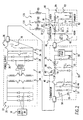
- FIG. 1 A first preferred embodiment of a pulse power system for an industrial narrow-band KrF excimer laser, is shown in block diagram form in FIG. 1.
- FIG. 2 A simplified combination block and circuit diagram of this preferred embodiment is shown in FIG. 2.
- the diagrams show a preferred embodiment built and tested by the Applicants for converting 208 volt three phase standard plant alternating current into 0.5 Joule to 6 Joule, 12 kv to 22 kv electrical pulses on a peaking capacitor of the excimer laser at pulse rates in the range of 2,000 Hz or greater.
- a system description is first provided below followed by a more detailed description of some of the important details of the individual modules and components of the system.
- This system is manufactured in four separate modules as indicated in FIGS. 1 and 2, each of which becomes an important part of the excimer laser system and each of which can be quickly replaced in the event of a parts failure or in the course of a regular preventative maintenance program.
- These modules are designated by Applicants: high voltage power supply module 20, commutator module 40, compression head module 60 and laser chamber module 80.
- High voltage power supply module 20 comprises a 300 volt rectifier 22 for converting the 208 volt three phase plant power from source 10 to 300 volt DC.
- Inverter 24 converts the output of rectifier 22 to high frequency 300 volt pulses in the range 100 kHz to 200 kHz. The frequency and the on period of inverter 24 are controlled by the HV power supply control board 21 in order to provide course regulation of the ultimate output pulse energy of the system.
- the output of inverter 24 is stepped up to about 1200 volts in step-up transformer 26.
- the output of transformer 26 is converted to 1200 volts DC by rectifier 28 which includes a standard bridge rectifier circuit 30 and a filter capacitor 32.
- HV power supply control board 21 which controls the operation of inverter 24 as shown in FIG. 1.
- Set points within HV power supply control board 21 are set by laser system control board 100.
- pulse energy control for the laser system is provided by power supply module 20.
- the electrical circuits in commutator 40 and compression head 60 merely serve to amplify and compress the electrical energy stored on charging capacitor 42 by power supply module 20.
- FIG. 1 indicates that control board 100 has controlled the power supply to provide 700 volts to charging capacitor 42 which during the charging cycle is isolated from the down stream circuits by solid state switch 46.
- Commutator module 40 comprises Co charging capacitor 42, which in this embodiment is a bank of capacitors connected in parallel to provide a total capacitance of 8.1 ⁇ F.
- Voltage divider 44 provides a feedback voltage signal to the HV power supply control board 21 which is used by control board 21 to limit the charging of capacitor 42 to the voltage (called the "control voltage") which when formed into an electrical pulse and compressed and amplified in commutator 40 and compression head 60 will produce the desired discharge voltage on peaking capacitor 82 and across electrodes 83 and 84.
- solid state switch 46 is a IGBT switch, although other switch technologies such as SCRs, GTOs, MCTs, etc. could also be used.
- a 600 nH charging inductor 48 is in series with solid state switch 46 to temporarily limit the current through switch 46 while it closes to discharge the Co charging capacitor 42.
- the charge on charging capacitor 42 is thus switched onto C 1 8.5 ⁇ F capacitor 52 in about 5 ⁇ s as shown on FIG. 6B.
- a saturable inductor 54 holds off the voltage on capacitor 52 and then becomes saturated allowing the transfer of charge from capacitor 52 through 1:23 step up pulse transformer 56 to C p-1 capacitor 62 in a transfer time period of about 550 ns, as shown on FIG. 6C, for a first stage of compression 61.
- pulse transformer 56 The design of pulse transformer 56 is described below. Performance wise the transformer is an extremely efficient pulse transformer, transforming a 700 volt 17,500 ampere 550 ns pulse rate into a 16,100 volt, 760 ampere 550 ns pulse which is stored very temporarily on C p-1 capacitor bank 62 in compression head module 60.
- Compression head module 60 further compresses the pulse.
- An L p-1 saturable inductor 64 (with about 125 nH saturated inductance) holds off the voltage on 16.5 nF C p-1 capacitor bank 62 for approximately 550 ns then allows the charge on C p-1 to flow (in about 100 ns) onto 16.5 nF Cp peaking capacitor 82 located on the top of laser chamber 80 and which is electrically connected in parallel with electrodes 83 and 84.
- This transformation of a 550 ns long pulse into a 100 ns long pulse to charge Cp peaking capacitor 82 makes up the second stage and last of compression as indicated at 65 on FIG. 1.
- the voltage on peaking capacitor 82 has reached about 14,000 volts and discharge between the electrodes begins.
- the discharge lasts about 50 ns during which time lasing occurs within the resonance chamber of the excimer laser.
- the resonance chamber is defined by a line narrowing package 86 comprised in this example by a 3-prism beam expander, a tuning mirror and an eschelle grating and an output coupler 88 which in this example, comprises a 10 percent R mirror.
- the laser pulse for this laser is a narrow band 20 ns 248 nm pulse of about 10 mJ and the repetition rate is 2000 pulses per second.
- the pulses define a laser beam 90 and the pulses of the beam are monitored by photodiode 92.
- the signal from photodiode 92 is transmitted to processor 102 in control board 100 and the processor uses this energy signal and preferably other historical pulse energy data to set the command voltage for the next and/or future pulses.
- processor 102 in control board 100 is programmed with a special algorithm which uses the most recent pulse energy signal along with the energy signal of all previous pulses in the burst along with other historical pulse profile data to select a control voltage for the subsequent pulse so as to minimized pulse-to-pulse energy variations and also to minimize burst-to-burst energy variations.
- This calculation is performed by processor 102 in control board 100 using this algorithm during a period of about 35 ⁇ s.
- the laser pulses occurs about 5 ⁇ s following the To firing of IGBT switch 46 shown on FIG. 6C and about 20 ⁇ s are required to collect the laser pulse energy data. (The start of the firing of switch 46 is called To.)
- a new control voltage value is thus ready (as shown on FIG. 6A) about 70 microseconds after the firing of IGBT switch 46 for the previous pulse (at 2,000 Hz the firing period is 500 ⁇ s).
- the features of this algorithm are described in greater detail in U.S. Patent Application Serial No. 09/034,870.
- This preferred embodiment is provided with electronic circuitry which recovers excess energy on charging capacitor 42 from the previous pulse which substantially reduces waste energy and virtually eliminates after ringing in the laser chamber 80.
- the energy recovery circuit 57 composed of energy recovery inductor 58 and energy recovery diode 59, the series combination of the two connected in parallel across Co charging capacitor 42. Because the impedance of the pulse power system is not exactly matched to that of the chamber and due to the fact that the chamber impedance varies several orders of magnitude during the pulse discharge, a negative going "reflection" is generated from the main pulse which propagates back towards the front end of the pulse generating system. After the excess energy has propagated back through the compression head 60 and the commutator 40, switch 46 opens up due to the removal of the trigger signal by the controller.
- the energy recovery circuit 57 reverses the polarity of the reflection which has generated a negative voltage on the charging capacitor 42 through resonant free wheeling (a half cycle of ringing of the L-C circuit made up of the charging capacitor 42 and the energy recovery inductor 58) as clamped against reversal of current in inductor 58 by diode 59.
- the net result is that substantially all of the reflected energy from the chamber 80 is recovered from each pulse and stored on charging capacitor 42 as a positive charge ready to be utilized for the next pulse.
- FIG. 6 is a time line chart showing the charges on capacitor Co, C 1 C p-1 and Cp. The chart shows the process of energy recovery on Co.
- a DC bias current is provided such that each inductor is reverse saturated at the time a pulse is initiated by the closing of switch 46.
- bias current flow of approximately 15A backwards (compared to the normal pulse current flow) through the inductors.
- This bias current is provided by bias current source 120 through isolation inductor Lbl.
- Actual current flow travels from the power supply through the ground connection of the commutator, through the primary winding of the pulse transformer, through saturable inductor 54, through saturable inductor 48, and through isolation inductor Lbl back to the bias current source 120 as indicated by arrows B1.
- a bias current B2 of approximate 5A is provided from the second bias current source 126 through isolation inductor Lb2.
- the current splits and the majority B2-1 goes through saturable inductor Lp-1 64 and back through isolation inductor Lb3 back to the second bias current source 126.
- a smaller fraction of the current B2-2 travels back through the HV cable connecting the compression head 60 and the commutator 40, through the pulse transformer secondary winding to ground, and through a biasing resistor back to the second bias current source 126.
- This second smaller current is used to bias the pulse transformer so that it is also reset for the pulsed operation.
- the amount of current which splits into each of the two legs is determined by the resistance in each path and is intentionally adjusted such that each path receives the correct amount of bias current.
- Co is charged with (for example) a positive 700 volts such that when switch 46 is closed current flows from capacitor 42 through inductor 48 in a direction toward C 1 capacitor 52 (which means that electrons are actually flowing in the reverse direction). Similarly, the current flow is from C 1 capacitor 52 through the primary side of pulse transformer 56 toward ground. Thus, the direction of current and pulse energy is the same from charging capacitor 42 to pulse transformer 56. As explained below under the section entitled "Pulse Transformer" current flow in both the primary loops and the secondary loop of pulse transformer 56 are both toward ground. The result is that current flow between pulse transformer 56 and the electrodes during discharge is in the direction away from the electrodes toward transformer 56.
- the direction of electron flow during discharge is from ground through the secondary of pulse transformer 56 temporarily onto C p-1 capacitor 62 through inductor 64, temporarily onto Cp capacitor 82, through inductor 81, through electrode 84 (which is the discharge cathode) through the discharge plasma, through electrode 83 and back to ground.
- pulse transformer 56 electrons flow in the same direction as the pulse energy during discharge.
- rectifier 22 is a 6 pulse phase controlled rectifier with a plus 150v to -150V DC output.
- Inverter 24 is actually three inverters 24A, 24B and 24C. Inverters 24B and 24C are turned off when the voltage on 8 ⁇ F Co charging capacitor 42 is 50 volts less than the command voltage and inverter 24A is turned off when the voltage on Co 42 slightly exceeds the command voltage. This procedure reduces the charge rate near the end of the charge.
- Step up transformers 26A, 26B and 26C are each rated at 7 kw and transform the voltage to 1200 volt AC.
- the HV power supply control board 21 converts a 12 bit digital command to an analog signal and compares it with a feedback signal 45 from Co voltage monitor 44.
- inverter 24A When the feedback voltage exceeds the command voltage, inverter 24A is turned off as discussed above, Q2 switch 34 closes to dissipate stored energy within the supply, Q3 isolation switch 36 opens to prevent any additional energy leaving the supply and Q1 bleed switch 38 closes to bleed down the voltage on Co 42 until the voltage on Co equals the command voltage. At that time Q 1 opens.
- FIGS. 1 and 2 The principal components of commutator 40 and compression head 60 are shown on FIGS. 1 and 2 and are discussed above with regard to the operation of the system. In this section, we describe details of fabrication of the commutator.
- Solid state switch 46 is an P/N CM 1000 HA-28H IGBT switch provided by Powerex, Inc. with offices in Youngwood, Pennsylvania.
- Inductors 48, 54 and 64 are saturable inductors similar to those described in U.S. Patents 5,448,580 and 5,315,611.
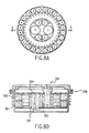
- a top and section view of the saturable inductor 64 is shown respectively in FIGS. 8A and 8B.
- flux excluding metal pieces 301, 302, 303 and 304 are added as shown in FIG. 8B in order to reduce the leakage flux in the inductors.
- These flux excluding pieces substantially reduce current flow through the inductor prior to saturation and greatly improves the pulse forming performance of the inductor in the system.
- the current makes four loops through vertical conductors.
- Capacitor banks 42, 52 and 62 are all comprised of banks of off-the-shelf capacitors connected in parallel. These capacitors are available from suppliers such as Murata with offices in Smyrna, Georgia. Applicants preferred method of connecting the capacitors and inductors is to bolt them to positive and negative terminals on special printed circuit board having heavy nickel coated copper leads in a manner similar to that described ins U.S. Patent No. 5,448,580.
- Pulse transformer 56 is also similar to the pulse transformer described in U.S. Patent Nos. 5,448,580 and 5,313,481; however, the pulse transformers of the present embodiment has only a single turn in the secondary winding and 23 primary windings.
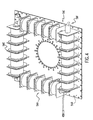
- a drawing of pulse transformer 56 is shown in FIG. 4.
- Each of the 23 primary windings comprise an aluminum spool 56A having two flanges (each with a flat edge with threaded bolt holes) which are bolted to positive and negative terminals on printed circuit board 56B as shown along the bottom edge of FIG. 4.
- Insulators 56C separates the positive terminal of each spool from the negative terminal of the adjacent spool.
- a hollow cylinder 1 1/16 inches long with a 0.875 OD with a wall thickness of about 1/32 inch.
- the spool is wrapped with one inch wide, 0.7 mil thick MetglasTM 2605 S3A and a 0.1 mil thick mylar film until the OD of the insulated MetglasTM wrapping is 2.24 inches.
- a prospective view of a single wrapped spool forming one primary winding is shown in FIG. 5.
- the secondary of the transformer is a single OD stainless steel rod mounted within a tight fitting insulating tube of electrical glass.
- the winding is in four sections as shown in FIG. 4.
- the stainless steel secondary shown as 56D in FIG. 4 is grounded to a ground lead on printed circuit board 56B at 56E and the high voltage terminal is shown at 56F.
- a 700 volt pulse between the + and - terminals of the primary windings will produce a minus 16,100 volt pulse at terminal 56F on the secondary side.
- This design provides very low leakage inductance permitting extremely fast output risetime.
- the Cp capacitor 82 is comprised of a bank of 28 0.59 nf capacitors mounted on top of the chamber pressure vessel. (Typically a KrF laser is operated with a lasing gas made up of 1.0% krypton, 0.1% fluorine, and the remainder neon.)
- the electrodes are each solid brass bars about 28 inches long which are separated by about 0.5 to 1.0 inch.
- the top electrode is the cathode and the bottom electrode is connected to ground as indicated in FIG. 1.
- Co is charged with a positive voltage and the flow of electrons is into the ground electrode of the laser chamber.
- the circuit can be easily reversed with Co charged to a negative charging voltage of about 700 volts and the electron flow will be from the ground electrode to the high voltage electrodes. Also reverse flow of electrons across the electrode gap could be accomplished by changing the polarity of the secondary winding (i.e., the four-section stainless steel tube).
- FIG. 7 shows a modification which would permit bi-polar operation of the laser.
- two power supplies are provided one supplying +1200 volts and the other providing -1200 volts.
- switch 46 is duplicated so that we have 46A and 46B.
- 46A When 46A is closed the polarity of system is like that described in detail above. However, with 46A open and switch 46B closes the resulting pulse is everywhere reversed and the electron flow across the discharge gap is from the ground electrode to the high voltage electrode (in this case about +14,000 volts). In this case, the energy recovery circuit 57 is not needed.
- Co A is charged to +700 v at To 46A will close allowing Co A to discharge through inductor 48 then it will open and 46B will close permitting the reflected energy to be recovered on Co B after recovery of the energy 46B opens. Then Co B is charged to -700 v and at the next To 46B closes allowing Co B to discharge through the circuit.
- the result is alternating discharge directions. This embodiment should provide for more even wear of the electrodes.
- FIG. 10 is a side section view of the laser system showing the location of the compressor lead module in relation to electrodes 83 and 84.
- This technique was designed to minimize the impedance associated with the compression lead chamber connection and at the same time facilitates quick replacement of the compression head.
- the ground connection is made with an approximately 28 inch long slot tab connection along the back side of the compression head as shown at 81 A in FIG. 10A and 81B in FIG. 10B.
- the top of the slot is fitted with flexible finger stock.
- a preferred finger stock material is sold under the trade name Multilam®.
- the high voltage connection is made between a six-inch diameter smooth bottom of saturable inductor 64 and a mating array of flexible finger stock at 89 in FIG. 10A.
- a preferred finger stock material is Multilam®. This arrangement permits the replacement of the compression head module for repair or preventative maintenance in about five minutes.
- oil leakage from electrical components has been a problem.
- oil insulated components are limited to the saturable inductors.
- the saturable inductors as shown in FIG. 8B are housed in a pot type oil containing housing in which all seal connections are located above the oil level to substantially eliminate the possibility of oil leakage.
- the lowest seal in inductor 64 is shown at 308 in FIG. 8B.
- the power supply module described for the first preferred embodiment which utilizes two rectifiers, an inverter and a transformer as shown in FIGS. 1 and 2; is replaced by an off-the-shelf power supply and a resonance charging circuit. This latter approach provides much faster charging of the charging capacitor.
- FIG 9A An electrical circuit showing this preferred embodiment is shown in FIG 9A.
- a standard capacitor charging power supply 200 having a 480 VAC/40 amp input and a 1200 VDC 50 amp output is used.
- Such power supplies are available from suppliers such as Ecgar, Maxwell, Kaiser and Ale.
- This power supply continuously charges a 325 ⁇ F capacitor 202 to the voltage level commanded by the control board 204.
- the control board 204 also commands IGBT switch 206 closed and open to transfer energy from capacitor 202 to capacitor 42.
- Inductor 208 sets up the transfer time constant in conjunction with capacitor 202 and 42.
- Control board 202 receives a voltage feedback 212 that is proportional to the voltage on capacitor 42 and a current feedback 214 that is proportional to the current flowing through inductor 208.
- control board 204 can calculate in real time the final voltage on capacitor 42 should IGBT switch 206 open at that instant of time. Therefore with a command voltage 210 fed into control board 204 a precise calculation can be made of the stored energy within capacitor 42 and inductor 208 to compare to the required charge voltage commanded 210. From this calculation, the control board 204 will determine the exact time in the charge cycle to open IGBT switch 206.
- IGBT switch 206 opens the energy stored in the magnetic field of inductor 208 will transfer to capacitor 42 through the diode path 216.
- the accuracy of the real time energy calculation will determine the amount of fluctuation dither that will exist on the final voltage on capacitor 42. Due to the extreme charge rate of this system, too much dither will exist to meet a desired systems regulation need of ⁇ 0.05%. Therefore a bleed down circuit is included in this embodiment
- Bleed down circuit 216 will be commanded closed by the control board 204 when current flowing through inductor 208 stops.
- the time constant of capacitor 42 and resistor 220 should be sufficiently fast to bleed down capacitor 42 to the command voltage 210 without being an appreciable amount of the total charge cycle.
- FIG. 9B A second resonant charger system is shown in FIG. 9B. This circuit is similar to the one shown in FIG. 9A.
- the principal circuit elements are:
- the power supply is a fixed 700-volt power supply.
- the power supply is attached directly to C-1 eliminating the need for voltage feedback to the supply.
- the performance of the system is independent of the voltage regulation on C-1 therefore only the most basic control loop is necessary in the power supply. Secondly the supply will be adding energy into the system whenever the voltage on C-1 falls below the 700-volt setting. This allows the power supply the entire time between laser pulse, (and even during laser pulses), to replenish energy transferred from C-1 to C0. This further reduces the power supply peak current requirements over the pulse power system described above. As can be seen in FIG. 6A the power supply is only given a percentage of the total time between laser pulses to charge C0 to a desired voltage. The combination of requiring a supply with the most basic control loop, and minimizing the peak current rating of the supply to the average power requirements of the system reduces the power supply cost an estimated 50%. Additionally this preferred design provides vendor flexibility since constant current, fixed output voltage power supplies are readily available from multiple sources.
- the reason for adding 100 volts to the calculation is to ensure current is still flowing in L1 at the time the voltage on C0 equals the command voltage.
- the maximum first pulse voltage on C0 will be 1400 volts.
- the maximum operating voltage will be 1200 volts. This allows the system to hold up to 200 volts of charge in L1 for reserve. This reserve can be incrementally pulsed onto C0 as needed due to leakage losses during the time after C0 equals the command voltage and the laser discharging C0.
Landscapes
- Physics & Mathematics (AREA)
- Electromagnetism (AREA)
- Engineering & Computer Science (AREA)
- Plasma & Fusion (AREA)
- Optics & Photonics (AREA)
- General Physics & Mathematics (AREA)
- Nonlinear Science (AREA)
- Lasers (AREA)
- Generation Of Surge Voltage And Current (AREA)
Claims (27)
- Pulsleistungsquelle für hohe Pulsraten mit der Bereitstellung gesteuerter elektrischer Pulse bei Raten von 2000 Hz oder höher, mit:a) einer Pulserzeugungsschaltung (40) mit:zum Erzeugen elektrischer Pulse mit elektrischer Energie mit mehr als 3 Joule und mit Spitzenspannungen über 600 Volt;1) einem Ladekondensator (42) zum Speichern einer Ladung bei Spannungen von über 600 Volt,2) einem Halbleiterschalter (46), der beim Schließen die Entladung des Ladekondensators bewirkt, und3) einer Strombegrenzungsinduktivität (48) in Reihe mit dem Halbleiterschalter, um temporär den Strom durch den Schalter beim Schließen zu begrenzen,b) mindestens zwei Pulskompressionsschaltungen, die eine erste Kompressionsschaltung (61) und eine zweite Kompressionsschaltung (65) definieren, wobei jede Kompressionsschaltung eine Kondensatorbank (62, 89) und eine sättigbare Induktivität (54, 64) aufweist und wobei die mindestens zwei Pulskompressionsschaltungen in Reihe verbunden sind;c) einem Hochsetzpulstransformator (56) zum Erhöhen der Spitzenspannung der elektrischen Pulse auf mindestens 12 000 Volt, wobei der Pulstransformator mehrere elektrisch parallele Primärwicklungen (56a) aufweist und wobei eine Sekundärwicklung mindestens einen im Wesentlichen geraden Leiter aufweist;d) eine sehr schnelle geregelte Leistungsversorgung (20) zum Laden des Ladekondensators (42) mit mindestens 3 Joule elektrischer Energie bei Spannungen von mindestens 600 Volt in weniger als 400 Mikrosekunden, unde) einem sehr schnellen Pulssteuerungssystem (100) mit einem Prozessor (102) zum Steuern des Ladens des Ladekondensators (42) mit einer Genauigkeitsabweichung von weniger als 1% bei einer Rate von mindestens 2000 Ladungen pro Sekunde.
- Pulsleistungsquelle nach Anspruch 1, wobei der Hochsetztransformator ein Teil der ersten Kompressionsschaltung ist.
- Pulsleistungsquelle nach Anspruch 1, wobei der mindestens eine im Wesentliche gerade Leiter vier gerade Stäbe aufweist, die elektrisch in Reihe geschaltet sind.
- Pulsleistungsquelle nach Anspruch 1, wobei die mehreren Primärwicklungen mindestens 20 Primärwicklungen sind.
- Pulsleistungsquelle nach Anspruch 1, wobei die geregelte Leistungsversorgung eine Entladungsschaltung mit einem Schalter (38) und einem Widerstand aufweist, um eine Spannung an dem Ladekondensator auf eine gewünschte Steuerspannung abzusenken.
- Pulsleistungsquelle nach Anspruch 1, wobei die Quelle eine Komponente eines elektrischen Entladungslasers (80) ist und elektrische Pulse erzeugt, um Entladungen zwischen Elektroden (83, 84) des Lasers zur Erzeugung von Laserpulsen mit jeweils einer definierten Pulsenergie zu erzeugen.
- Pulsleistungsquelle nach Anspruch 6, die ferner einen Pulsenergiemonitor (92) zum Überwachen der Energie der Laserpulse umfasst.
- Pulsleistungsquelle nach Anspruch 7, wobei der Prozessor zum Steuern des Ladens des Ladekondensators mit einem Algorithmus programmiert ist, um eine Steuerspannung für einen Puls auf der Grundlage der Pulsenergie mindestens eines vorhergehenden Pulses zu berechnen.
- Pulsleistungsquelle nach Anspruch 8, wobei der mindestens eine vorhergehende Puls die gesamten Pulse aus einer Pulssequenz umfasst.
- Pulsleistungsquelle nach Anspruch 9, wobei der mindestens eine Puls ferner Pulse von früheren Pulssequenzen umfasst.
- Pulsleistungsquelle nach Anspruch 1, wobei die mindestens zwei Kompressionsschaltungen zwei Kompressionsschaltungen sind und der Kondensator in der zweiten Kompressionsschaltung ein Spitzenkondensator ist.
- Pulsleistungsquelle nach Anspruch 1, wobei die Pulserzeugungsschaltung, die Kompressionsschaltungen, der Pulstransformator und die Leistungsversorgung als Module hergestellt sind und Komponenten eines elektrischen Entladungslasersystems mit zwei Elektroden bilden.
- Pulsleistungsquelle nach Anspruch 12, wobei das Lasersystem ein Excimerlasersystem ist.
- Pulsleistungssystem nach Anspruch 13, wobei der Excimerlaser ein KrF-Lasersystem ist.
- Pulsleistungssystem nach Anspruch 12, wobei die Module luftgekühlt sind.
- Pulsleistungssystem nach Anspruch 12, wobei die sättigbaren Induktivitäten in Transformatoröl eingetaucht sind, das einen Ölstand in einem topfähnlichen Behälter definiert mit mindestens einem Dichtübergang, wobei der Ölpegel unterhalb des mindestens einen Dichtübergangs liegt.
- Pulsleistungssystem nach Anspruch 1, wobei mindestens eine der sättigbaren Induktivitäten zumindest einen Bereich (301, 302, 303, 305) ohne Fluss aufweist.
- Pulsleistungssystem nach Anspruch 1, wobei der Kondensator und die Induktivitäten elektrisch unter Verwendung kupferbeschichteter gedruckter Leiterplatten und Bolzen zum Verbinden der Kondensatoren und der Induktivitäten mit den gedruckten Leiterplatten verbunden sind.
- Pulsleistungssystem nach Anspruch 12, wobei eine der beiden Elektroden mit Masse verbunden ist und wobei das Pulsleistungssystem eine negative Hochspannung der anderen der beiden Elektroden zuführt.
- Pulsleistungssystem nach Anspruch 12, wobei eine der beiden Elektroden mit Masse verbunden ist, und das Pulsleistungssystem eine positive Hochspannung der anderen der beiden Elektroden zuführt.
- Pulsleistungssystem nach Anspruch 12, wobei die Pulserzeugungsschaltung eine Pulserzeugungsschaltung zum Erzeugen negativer Pulse ist und ferner eine zweite Pulserzeugungsschaltung für die Erzeugung positiver Pulse vorgesehen ist, wobei die erste Pulserzeugungsschaltung und die zweite Pulserzeugungsschaltung so gesteuert werden, um abwechselnd Pulse zu erzeugen, um einen bipolaren Betrieb des elektrischen Entladungslasers zu bewirken.
- Pulsleistungssystem nach Anspruch 13, wobei das Excimerlasersystem ein ArF-Lasersystem ist.
- Pulsleistungsquelle mit hoher Pulsrate nach Anspruch 1, wobei die sehr schnelle Leistungsversorgung eine Leistungsversorgungsresonanzschaltung umfasst mit:a) einem Quellenkondensator (32) mit einer Kapazität, die mindestens 5 x der Kapazität des Ladekondensators entspricht;b) einer Gleichspannungsleistungsversorgung (22, 24, 26, 30) mit einer Nennlast von mindestens 7 kW zum Bereitstellen elektrischer Leistung bei mindestens 300 Volt für den Quellenkondensator;c) einer strombegrenzenden Leistungsversorgungsinduktivität für das Begrenzen des Stromflusses von dem Quellenkondensator zu dem Ladekondensator;d) einem Halbleiterschalter (36), der mit dem Quellenkondensator, der strombegrenzenden Leistungsversorgungsinduktivität und dem Ladekondensator in Reihe geschaltet ist, wobei der Ladekondensator durch Schließen des Halbleiterschalters geladen wird.
- Pulsleistungsquelle mit hoher Pulsrate nach Anspruch 23, wobei die Leistungsversorgungsresonanzschaltung ferner eine Entladeschaltung zum Absenken der Spannung auf dem Ladekondensator bis herunter zu einem vorbestimmten Sollwert aufweist.
- Pulsleistungsquelle mit hoher Pulsrate nach Anspruch 23, wobei die Leistungsversorgungsresonanzschaltung ferner eine Freilaufstromschleife aufweist, die die strombegrenzende Leistungsversorgungsinduktivität, eine Diode und einen Halbleiterfreilaufstromschalter aufweist.
- Pulsleistungsquelle mit hoher Pulsrate nach Anspruch 25, wobei der Prozessor so programmiert ist, um den Freilaufstromschleifenschalter zu schließen, wenn eine Spannung an dem Ladekondensator auf einen ersten vorbestimmten Wert ansteigt.
- Pulsleistungsquelle mit hoher Pulsrate nach Anspruch 26, wobei der Prozessor ferner programmiert ist, um den Freilaufstromschleifenschalter zu öffnen, wenn die Spannung an dem Ladekondensator auf einen zweiten vorbestimmten Wert abfällt.
Applications Claiming Priority (7)
| Application Number | Priority Date | Filing Date | Title |
|---|---|---|---|
| US08/990,848 US5940421A (en) | 1997-12-15 | 1997-12-15 | Current reversal prevention circuit for a pulsed gas discharge laser |
| US990848 | 1997-12-15 | ||
| US08/995,832 US5982795A (en) | 1997-12-22 | 1997-12-22 | Excimer laser having power supply with fine digital regulation |
| US995832 | 1997-12-22 | ||
| US118773 | 1998-07-18 | ||
| US09/118,773 US5936988A (en) | 1997-12-15 | 1998-07-18 | High pulse rate pulse power system |
| PCT/US1998/026602 WO1999031773A1 (en) | 1997-12-15 | 1998-12-15 | High pulse rate pulse power system |
Publications (3)
| Publication Number | Publication Date |
|---|---|
| EP1040539A1 EP1040539A1 (de) | 2000-10-04 |
| EP1040539A4 EP1040539A4 (de) | 2002-09-18 |
| EP1040539B1 true EP1040539B1 (de) | 2004-11-10 |
Family
ID=27382215
Family Applications (1)
| Application Number | Title | Priority Date | Filing Date |
|---|---|---|---|
| EP98963922A Expired - Lifetime EP1040539B1 (de) | 1997-12-15 | 1998-12-15 | Gepulstes stromversorgungssystem mit hoher pulsrate |
Country Status (6)
| Country | Link |
|---|---|
| US (1) | US6028872A (de) |
| EP (1) | EP1040539B1 (de) |
| JP (1) | JP3725781B2 (de) |
| AU (1) | AU1915099A (de) |
| DE (1) | DE69827524T2 (de) |
| WO (1) | WO1999031773A1 (de) |
Families Citing this family (48)
| Publication number | Priority date | Publication date | Assignee | Title |
|---|---|---|---|---|
| US6240112B1 (en) * | 1997-12-15 | 2001-05-29 | Cymer, Inc. | High pulse rate pulse power system with liquid cooling |
| US6151346A (en) * | 1997-12-15 | 2000-11-21 | Cymer, Inc. | High pulse rate pulse power system with fast rise time and low current |
| US6381256B1 (en) | 1999-02-10 | 2002-04-30 | Lambda Physik Ag | Molecular fluorine laser with spectral linewidth of less than 1 pm |
| US6490307B1 (en) | 1999-03-17 | 2002-12-03 | Lambda Physik Ag | Method and procedure to automatically stabilize excimer laser output parameters |
| US6424666B1 (en) | 1999-06-23 | 2002-07-23 | Lambda Physik Ag | Line-narrowing module for high power laser |
| US6650679B1 (en) | 1999-02-10 | 2003-11-18 | Lambda Physik Ag | Preionization arrangement for gas laser |
| US6456643B1 (en) | 1999-03-31 | 2002-09-24 | Lambda Physik Ag | Surface preionization for gas lasers |
| US6618421B2 (en) * | 1998-07-18 | 2003-09-09 | Cymer, Inc. | High repetition rate gas discharge laser with precise pulse timing control |
| US6757315B1 (en) | 1999-02-10 | 2004-06-29 | Lambda Physik Ag | Corona preionization assembly for a gas laser |
| US6965624B2 (en) * | 1999-03-17 | 2005-11-15 | Lambda Physik Ag | Laser gas replenishment method |
| US6463086B1 (en) | 1999-02-10 | 2002-10-08 | Lambda Physik Ag | Molecular fluorine laser with spectral linewidth of less than 1 pm |
| US6389052B2 (en) | 1999-03-17 | 2002-05-14 | Lambda Physik Ag | Laser gas replenishment method |
| US6421365B1 (en) | 1999-11-18 | 2002-07-16 | Lambda Physik Ag | Narrow band excimer or molecular fluorine laser having an output coupling interferometer |
| US6546037B2 (en) | 1999-02-10 | 2003-04-08 | Lambda Physik Ag | Molecular fluorine laser with spectral linewidth of less than 1 pm |
| US6727731B1 (en) | 1999-03-12 | 2004-04-27 | Lambda Physik Ag | Energy control for an excimer or molecular fluorine laser |
| US6700915B2 (en) | 1999-03-12 | 2004-03-02 | Lambda Physik Ag | Narrow band excimer laser with a resonator containing an optical element for making wavefront corrections |
| DE29907349U1 (de) | 1999-04-26 | 2000-07-06 | Lambda Physik Gesellschaft zur Herstellung von Lasern mbH, 37079 Göttingen | Laser zur Erzeugung schmalbandiger Strahlung |
| US6785316B1 (en) | 1999-08-17 | 2004-08-31 | Lambda Physik Ag | Excimer or molecular laser with optimized spectral purity |
| US6553050B1 (en) | 1999-11-18 | 2003-04-22 | Lambda Physik Ag | Narrow band excimer or molecular fluorine laser having an output coupling interferometer |
| US6603788B1 (en) | 1999-11-23 | 2003-08-05 | Lambda Physik Ag | Resonator for single line selection |
| JP2003521683A (ja) | 2000-01-25 | 2003-07-15 | ラムダ フィジーク アーゲー | ビーム・パラメータ監視ユニット、分子弗素(F2)或はArFレーザ・システム、分子弗素(F2)レーザ・システム、およびArFレーザ・システム |
| US6735232B2 (en) | 2000-01-27 | 2004-05-11 | Lambda Physik Ag | Laser with versatile output energy |
| US7075963B2 (en) | 2000-01-27 | 2006-07-11 | Lambda Physik Ag | Tunable laser with stabilized grating |
| US6834066B2 (en) | 2000-04-18 | 2004-12-21 | Lambda Physik Ag | Stabilization technique for high repetition rate gas discharge lasers |
| US6862307B2 (en) | 2000-05-15 | 2005-03-01 | Lambda Physik Ag | Electrical excitation circuit for a pulsed gas laser |
| US6711202B2 (en) * | 2000-06-09 | 2004-03-23 | Cymer, Inc. | Discharge laser with porous insulating layer covering anode discharge surface |
| US6763049B1 (en) | 2000-06-15 | 2004-07-13 | Lambda Emi | Very high repetition rate power supply system and method |
| US6577663B2 (en) | 2000-06-19 | 2003-06-10 | Lambda Physik Ag | Narrow bandwidth oscillator-amplifier system |
| JP4079585B2 (ja) * | 2000-10-12 | 2008-04-23 | オリジン電気株式会社 | コンデンサの充電方法及び充電装置 |
| US6384579B2 (en) | 2000-06-27 | 2002-05-07 | Origin Electric Company, Limited | Capacitor charging method and charging apparatus |
| US6603789B1 (en) | 2000-07-05 | 2003-08-05 | Lambda Physik Ag | Narrow band excimer or molecular fluorine laser with improved beam parameters |
| US6807205B1 (en) | 2000-07-14 | 2004-10-19 | Lambda Physik Ag | Precise monitor etalon calibration technique |
| US6721345B2 (en) | 2000-07-14 | 2004-04-13 | Lambda Physik Ag | Electrostatic precipitator corona discharge ignition voltage probe for gas status detection and control system for gas discharge lasers |
| US6671302B2 (en) | 2000-08-11 | 2003-12-30 | Lambda Physik Ag | Device for self-initiated UV pre-ionization of a repetitively pulsed gas laser |
| US6801561B2 (en) | 2000-09-25 | 2004-10-05 | Lambda Physik Ag | Laser system and method for spectral narrowing through wavefront correction |
| JP3755577B2 (ja) * | 2000-10-10 | 2006-03-15 | ウシオ電機株式会社 | 露光用ArF、KrFエキシマレーザ装置及びフッ素レーザ装置 |
| US6747741B1 (en) | 2000-10-12 | 2004-06-08 | Lambda Physik Ag | Multiple-pass interferometric device |
| JP3589996B2 (ja) | 2001-03-27 | 2004-11-17 | オリジン電気株式会社 | コンデンサ充電方法及びコンデンサ充電器 |
| US6998620B2 (en) * | 2001-08-13 | 2006-02-14 | Lambda Physik Ag | Stable energy detector for extreme ultraviolet radiation detection |
| JP3701015B2 (ja) | 2001-10-30 | 2005-09-28 | オリジン電気株式会社 | コンデンサの充電方法及びその充電装置 |
| US8379687B2 (en) | 2005-06-30 | 2013-02-19 | Cymer, Inc. | Gas discharge laser line narrowing module |
| US7706424B2 (en) * | 2005-09-29 | 2010-04-27 | Cymer, Inc. | Gas discharge laser system electrodes and power supply for delivering electrical energy to same |
| US7321607B2 (en) | 2005-11-01 | 2008-01-22 | Cymer, Inc. | External optics and chamber support system |
| CN101924489B (zh) * | 2009-12-31 | 2013-07-31 | 周云正 | 非热等离子体脉冲电源 |
| WO2014017562A1 (ja) * | 2012-07-26 | 2014-01-30 | ギガフォトン株式会社 | レーザ装置及びレーザ装置の制御方法 |
| CN104601033B (zh) * | 2015-02-06 | 2017-12-15 | 中国人民解放军信息工程大学 | 高压脉冲型磁控管电源 |
| WO2018195454A1 (en) * | 2017-04-20 | 2018-10-25 | De Rochemont L Pierre | Resonant high energy density storage device |
| EP3925056A1 (de) | 2019-02-13 | 2021-12-22 | Sew-Eurodrive GmbH & Co. KG | System zur berührungslosen übertragung elektrische leistung an ein mobilteil |
Family Cites Families (17)
| Publication number | Priority date | Publication date | Assignee | Title |
|---|---|---|---|---|
| US4258334A (en) * | 1976-05-17 | 1981-03-24 | Sri International | Noble gas-halogen transfer laser method and means |
| US4710939A (en) * | 1983-07-23 | 1987-12-01 | Quantum Diagnostics Ltd. | X-ray frequency down converter |
| US4549091A (en) * | 1983-08-08 | 1985-10-22 | Standard Oil Company (Indiana) | Electrical excitation circuit for gas lasers |
| US4611327A (en) * | 1983-11-25 | 1986-09-09 | Amoco Corporation | Gas transport laser system |
| US4606034A (en) * | 1985-02-19 | 1986-08-12 | Board Of Trustees, University Of Illinois | Enhanced laser power output |
| CA1298959C (en) * | 1985-09-28 | 1992-04-21 | Kohzo Hakuta | Method of refining rare gas halide excimer laser gas |
| US5142543A (en) * | 1988-01-27 | 1992-08-25 | Kabushiki Kaisha Komatsu Seisakusho | Method and system for controlling narrow-band oscillation excimer laser |
| JPH03504429A (ja) * | 1988-04-20 | 1991-09-26 | シーメンス アクチェンゲゼルシヤフト | 特にteガスレーザー用の高出力の高電圧パルス発生装置および方法 |
| JPH0760914B2 (ja) * | 1989-01-30 | 1995-06-28 | セントラル硝子株式会社 | エキシマーレーザーガスの精製法並びにその装置 |
| US5463650A (en) * | 1992-07-17 | 1995-10-31 | Kabushiki Kaisha Komatsu Seisakusho | Apparatus for controlling output of an excimer laser device |
| US5313481A (en) * | 1993-09-29 | 1994-05-17 | The United States Of America As Represented By The United States Department Of Energy | Copper laser modulator driving assembly including a magnetic compression laser |
| JP2631080B2 (ja) * | 1993-10-05 | 1997-07-16 | 株式会社小松製作所 | レーザ装置の出力制御装置 |
| JP2816813B2 (ja) * | 1994-04-12 | 1998-10-27 | 株式会社小松製作所 | エキシマレーザ装置 |
| US5448580A (en) * | 1994-07-05 | 1995-09-05 | The United States Of America As Represented By The United States Department Of Energy | Air and water cooled modulator |
| DE69628514T2 (de) * | 1995-02-17 | 2004-04-29 | Cymer, Inc., San Diego | Leistungspulsgenerator mit energierückgewinnung |
| US5936988A (en) * | 1997-12-15 | 1999-08-10 | Cymer, Inc. | High pulse rate pulse power system |
| US5940421A (en) * | 1997-12-15 | 1999-08-17 | Cymer, Inc. | Current reversal prevention circuit for a pulsed gas discharge laser |
-
1998
- 1998-12-15 EP EP98963922A patent/EP1040539B1/de not_active Expired - Lifetime
- 1998-12-15 AU AU19150/99A patent/AU1915099A/en not_active Abandoned
- 1998-12-15 JP JP2000539559A patent/JP3725781B2/ja not_active Expired - Fee Related
- 1998-12-15 DE DE69827524T patent/DE69827524T2/de not_active Expired - Lifetime
- 1998-12-15 US US09/211,825 patent/US6028872A/en not_active Expired - Lifetime
- 1998-12-15 WO PCT/US1998/026602 patent/WO1999031773A1/en not_active Ceased
Also Published As
| Publication number | Publication date |
|---|---|
| DE69827524T2 (de) | 2005-04-07 |
| JP2002509363A (ja) | 2002-03-26 |
| JP3725781B2 (ja) | 2005-12-14 |
| WO1999031773A1 (en) | 1999-06-24 |
| US6028872A (en) | 2000-02-22 |
| EP1040539A4 (de) | 2002-09-18 |
| AU1915099A (en) | 1999-07-05 |
| EP1040539A1 (de) | 2000-10-04 |
| DE69827524D1 (de) | 2004-12-16 |
Similar Documents
| Publication | Publication Date | Title |
|---|---|---|
| EP1040539B1 (de) | Gepulstes stromversorgungssystem mit hoher pulsrate | |
| EP1101258B1 (de) | Pulsgeneratorsystem mit hoher pulsrate | |
| US6151346A (en) | High pulse rate pulse power system with fast rise time and low current | |
| US6240112B1 (en) | High pulse rate pulse power system with liquid cooling | |
| US6018537A (en) | Reliable, modular, production quality narrow-band high rep rate F2 laser | |
| US6782031B1 (en) | Long-pulse pulse power system for gas discharge laser | |
| WO1999060679A1 (en) | Reliable modular production quality narrow-band high rep rate f2 laser | |
| USRE38054E1 (en) | Reliable, modular, production quality narrow-band high rep rate F2 laser | |
| KR100343032B1 (ko) | 적색 가시광 및 ir 제어부를 구비한 f2 레이저 | |
| TW393816B (en) | High pulse rate pulse power system | |
| JP2005150526A (ja) | 電源装置および高電圧パルス発生装置並びに放電励起式ガスレーザ装置 | |
| TW412891B (en) | Reliable modular production quality narrow-band high rep rate F2 laser | |
| KR20240088911A (ko) | 레이저 전극을 컨디셔닝하기 위한 장치 및 방법 | |
| EP1821377A2 (de) | Gasentladungslasersystem |
Legal Events
| Date | Code | Title | Description |
|---|---|---|---|
| PUAI | Public reference made under article 153(3) epc to a published international application that has entered the european phase |
Free format text: ORIGINAL CODE: 0009012 |
|
| 17P | Request for examination filed |
Effective date: 20000614 |
|
| AK | Designated contracting states |
Kind code of ref document: A1 Designated state(s): DE FR GB NL |
|
| A4 | Supplementary search report drawn up and despatched |
Effective date: 20020806 |
|
| AK | Designated contracting states |
Kind code of ref document: A4 Designated state(s): DE FR GB NL |
|
| RIC1 | Information provided on ipc code assigned before grant |
Free format text: 7H 01S 3/097 A, 7H 01S 3/0971 B |
|
| GRAP | Despatch of communication of intention to grant a patent |
Free format text: ORIGINAL CODE: EPIDOSNIGR1 |
|
| RAP1 | Party data changed (applicant data changed or rights of an application transferred) |
Owner name: CYMER, INC. |
|
| GRAS | Grant fee paid |
Free format text: ORIGINAL CODE: EPIDOSNIGR3 |
|
| GRAA | (expected) grant |
Free format text: ORIGINAL CODE: 0009210 |
|
| AK | Designated contracting states |
Kind code of ref document: B1 Designated state(s): DE FR GB NL |
|
| REG | Reference to a national code |
Ref country code: GB Ref legal event code: FG4D |
|
| REF | Corresponds to: |
Ref document number: 69827524 Country of ref document: DE Date of ref document: 20041216 Kind code of ref document: P |
|
| ET | Fr: translation filed | ||
| PLBE | No opposition filed within time limit |
Free format text: ORIGINAL CODE: 0009261 |
|
| STAA | Information on the status of an ep patent application or granted ep patent |
Free format text: STATUS: NO OPPOSITION FILED WITHIN TIME LIMIT |
|
| 26N | No opposition filed |
Effective date: 20050811 |
|
| REG | Reference to a national code |
Ref country code: DE Ref legal event code: R082 Ref document number: 69827524 Country of ref document: DE Representative=s name: GRUENECKER PATENT- UND RECHTSANWAELTE PARTG MB, DE Ref country code: DE Ref legal event code: R081 Ref document number: 69827524 Country of ref document: DE Owner name: CYMER, LLC (N.D.GES. D.STAATES NEVADA), SAN DI, US Free format text: FORMER OWNER: CYMER, INC., SAN DIEGO, CALIF., US |
|
| REG | Reference to a national code |
Ref country code: FR Ref legal event code: PLFP Year of fee payment: 18 |
|
| PGFP | Annual fee paid to national office [announced via postgrant information from national office to epo] |
Ref country code: GB Payment date: 20151221 Year of fee payment: 18 Ref country code: DE Payment date: 20151211 Year of fee payment: 18 |
|
| PGFP | Annual fee paid to national office [announced via postgrant information from national office to epo] |
Ref country code: NL Payment date: 20151221 Year of fee payment: 18 Ref country code: FR Payment date: 20151221 Year of fee payment: 18 |
|
| REG | Reference to a national code |
Ref country code: FR Ref legal event code: TP Owner name: CYMER, LLC, US Effective date: 20160615 |
|
| REG | Reference to a national code |
Ref country code: GB Ref legal event code: 732E Free format text: REGISTERED BETWEEN 20160811 AND 20160817 |
|
| REG | Reference to a national code |
Ref country code: NL Ref legal event code: PD Owner name: KONA TECHNOLOGIES LLC; US Free format text: DETAILS ASSIGNMENT: VERANDERING VAN EIGENAAR(S), SAMENVOEGEN; FORMER OWNER NAME: CYMER, INC. Effective date: 20160930 Ref country code: NL Ref legal event code: HC Owner name: CYMER LLC; US Free format text: DETAILS ASSIGNMENT: VERANDERING VAN EIGENAAR(S), VERANDERING VAN NAAM VAN DE EIGENAAR(S); FORMER OWNER NAME: KONA TECHNOLOGIES LLC Effective date: 20160930 |
|
| REG | Reference to a national code |
Ref country code: DE Ref legal event code: R119 Ref document number: 69827524 Country of ref document: DE |
|
| REG | Reference to a national code |
Ref country code: NL Ref legal event code: MM Effective date: 20170101 |
|
| GBPC | Gb: european patent ceased through non-payment of renewal fee |
Effective date: 20161215 |
|
| PG25 | Lapsed in a contracting state [announced via postgrant information from national office to epo] |
Ref country code: NL Free format text: LAPSE BECAUSE OF NON-PAYMENT OF DUE FEES Effective date: 20170101 |
|
| REG | Reference to a national code |
Ref country code: FR Ref legal event code: ST Effective date: 20170831 |
|
| PG25 | Lapsed in a contracting state [announced via postgrant information from national office to epo] |
Ref country code: FR Free format text: LAPSE BECAUSE OF NON-PAYMENT OF DUE FEES Effective date: 20170102 |
|
| PG25 | Lapsed in a contracting state [announced via postgrant information from national office to epo] |
Ref country code: GB Free format text: LAPSE BECAUSE OF NON-PAYMENT OF DUE FEES Effective date: 20161215 Ref country code: DE Free format text: LAPSE BECAUSE OF NON-PAYMENT OF DUE FEES Effective date: 20170701 |