EP1038360B1 - Empfänger mit programmierbaren dynamikbereich - Google Patents
Empfänger mit programmierbaren dynamikbereich Download PDFInfo
- Publication number
- EP1038360B1 EP1038360B1 EP98960824A EP98960824A EP1038360B1 EP 1038360 B1 EP1038360 B1 EP 1038360B1 EP 98960824 A EP98960824 A EP 98960824A EP 98960824 A EP98960824 A EP 98960824A EP 1038360 B1 EP1038360 B1 EP 1038360B1
- Authority
- EP
- European Patent Office
- Prior art keywords
- signal
- dynamic range
- adc
- receiver
- loop
- Prior art date
- Legal status (The legal status is an assumption and is not a legal conclusion. Google has not performed a legal analysis and makes no representation as to the accuracy of the status listed.)
- Expired - Lifetime
Links
Images


Classifications
-
- H—ELECTRICITY
- H04—ELECTRIC COMMUNICATION TECHNIQUE
- H04B—TRANSMISSION
- H04B1/00—Details of transmission systems, not covered by a single one of groups H04B3/00 - H04B13/00; Details of transmission systems not characterised by the medium used for transmission
- H04B1/06—Receivers
- H04B1/10—Means associated with receiver for limiting or suppressing noise or interference
- H04B1/1027—Means associated with receiver for limiting or suppressing noise or interference assessing signal quality or detecting noise/interference for the received signal
-
- H—ELECTRICITY
- H03—ELECTRONIC CIRCUITRY
- H03M—CODING; DECODING; CODE CONVERSION IN GENERAL
- H03M3/00—Conversion of analogue values to or from differential modulation
- H03M3/30—Delta-sigma modulation
- H03M3/458—Analogue/digital converters using delta-sigma modulation as an intermediate step
- H03M3/478—Means for controlling the correspondence between the range of the input signal and the range of signals the converter can handle; Means for out-of-range indication
- H03M3/488—Means for controlling the correspondence between the range of the input signal and the range of signals the converter can handle; Means for out-of-range indication using automatic control
-
- H—ELECTRICITY
- H04—ELECTRIC COMMUNICATION TECHNIQUE
- H04B—TRANSMISSION
- H04B1/00—Details of transmission systems, not covered by a single one of groups H04B3/00 - H04B13/00; Details of transmission systems not characterised by the medium used for transmission
- H04B1/06—Receivers
- H04B1/10—Means associated with receiver for limiting or suppressing noise or interference
- H04B1/109—Means associated with receiver for limiting or suppressing noise or interference by improving strong signal performance of the receiver when strong unwanted signals are present at the receiver input
-
- H—ELECTRICITY
- H03—ELECTRONIC CIRCUITRY
- H03M—CODING; DECODING; CODE CONVERSION IN GENERAL
- H03M3/00—Conversion of analogue values to or from differential modulation
- H03M3/30—Delta-sigma modulation
- H03M3/39—Structural details of delta-sigma modulators, e.g. incremental delta-sigma modulators
- H03M3/402—Arrangements specific to bandpass modulators
- H03M3/404—Arrangements specific to bandpass modulators characterised by the type of bandpass filters used
-
- H—ELECTRICITY
- H03—ELECTRONIC CIRCUITRY
- H03M—CODING; DECODING; CODE CONVERSION IN GENERAL
- H03M3/00—Conversion of analogue values to or from differential modulation
- H03M3/30—Delta-sigma modulation
- H03M3/39—Structural details of delta-sigma modulators, e.g. incremental delta-sigma modulators
- H03M3/412—Structural details of delta-sigma modulators, e.g. incremental delta-sigma modulators characterised by the number of quantisers and their type and resolution
- H03M3/414—Structural details of delta-sigma modulators, e.g. incremental delta-sigma modulators characterised by the number of quantisers and their type and resolution having multiple quantisers arranged in cascaded loops, each of the second and further loops processing the quantisation error of the loop preceding it, i.e. multiple stage noise shaping [MASH] type
Definitions
- the present invention relates to communications. More particularly, the present invention relates to a novel and improved programmable dynamic range receiver.
- High performance is required for many applications. High performance can be described by the linearity of the active devices (e.g. amplifiers, mixers, etc.) and the noise figure of the receiver. Second, for some applications such as in a cellular communication system, power consumption is an important consideration because of the portable nature of the receiver. Generally, high performance and high efficiency are conflicting design considerations.
- Most communication systems are narrow band systems which operate on an input RF signal having a predetermined bandwidth and center frequency.
- the input RF signal typically comprises other spurious signals located throughout the frequency spectrum. Non-linearity within the active devices causes intermodulation of spurious signals, resulting in products which may fall into the signal band.
- Second order non-linearity produces products at the sum and difference frequencies.
- spurious signals which can produce in-band second-order products are located far away from the signal band and can be easily filtered.
- third order non-linearity are more problematic.
- near band spurious signals (which are difficult to filter) can produce third order intermodulation products falling in-band, causing degradation in the received signal.
- the amplitude of the third-order products are scaled by g 1 •g 2 2 and g 1 2 •g 2 .
- every doubling of the amplitude of the spurious signals produces an eight-fold increase in the amplitude of the third order products.
- every 1 dB increase in the input RF signal results in 1 dB increase in the output RF signal but 3 dB increase in the third order products.
- the linearity of a receiver can be characterized by the input-referred third-order intercept point (IIP3).
- IIP3 input-referred third-order intercept point
- the output RF signal and the third-order intermodulation products are plotted versus the input RF signal.
- the IIP3 is a theoretical point where the desired output RF signal and the third-order products become equal in amplitude.
- the IIP3 is an extrapolated value since the active device goes into compression before the IIP3 point is reached.
- the calculation in equation (2) can be carried out in sequential order for subsequent stages within the receiver.
- N ⁇ F d S ⁇ N ⁇ R i ⁇ n - S ⁇ N ⁇ R out , where NF d is the noise figure of the active device, SNR in is the signal-to-noise ratio of the input RF signal into the active device, SNR out is signal-to-noise ratio of the output RF signal from the active device, and NF d , SNR in and SNR out are all given in decibel (dB).
- NF d decibel
- the gain of the active device can affect the noise figure of the subsequent stages. Similar to the IIP3 calculation in equation (2), the noise figure calculation in equation (4) can be carried out in sequential order for subsequent stages of the receiver.
- Receivers are employed for many communication applications, such as cellular communication systems and high definition television (HDTV).
- exemplary cellular communication systems include Code Division Multiple Access (CDMA) communication systems, Time Division Multiple Access (TDMA) communication systems, and analog FM communication systems.
- CDMA Code Division Multiple Access
- TDMA Time Division Multiple Access
- analog FM communication systems analog FM communication systems.
- CDMA Code Division Multiple Access
- FM-based transmission can cause jammers to appear within the allocated CDMA band and very close to the received CDMA signal.
- the amplitude of the jammers can be many time greater than that of the CDMA signal.
- the receiver is designed to have high IIP3.
- design of a high IIP3 receiver requires the active devices within the receiver to be biased with high DC current, thereby consuming large amounts of power. This design approach is especially undesirable for cellular application wherein the receiver is a portable unit and power is limited.
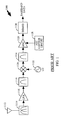
- FIG. 1 An exemplary block diagram of a receiver architecture of the prior art is shown in FIG. 1.
- the transmitted RF signal is received by antenna 1112, routed through duplexer 1114, and provided to low noise amplifier (LNA) 1116.
- LNA 1116 amplifies the RF signal and provides the signal to bandpass filter 1118.
- Bandpass filter 1118 filters the signal to remove some of the spurious signals which can cause intermodulation products in the subsequent stages.
- the filtered signal is provided to mixer 1120 which downconverts the signal to an intermediate frequency (IF) with the sinusoidal from local oscillator 1122.
- the IF signal is provided to bandpass filter 1124 which filters spurious signals and downconversion products prior to the subsequent downconversion stage.
- the filtered IF signal is provided to automatic-gain-control (AGC) amplifier 1126 which amplifies the signal with a variable gain to provide an IF signal at the required amplitude.
- the gain is controlled by a control signal from AGC control circuit 1128.
- the IF signal is provided to demodulator 1130 which demodulates the signal in accordance with the modulation format used at the transmitter.
- demodulator 1130 demodulates the signal in accordance with the modulation format used at the transmitter.
- BPSK binary phase shift keying
- QPSK quaternary phase shift keying
- OFQPSK offset quaternary phase shift keying
- QAM quadrature amplitude modulation
- a digital demodulator is used to provide the digitized baseband data.
- FM demodulator is used to provide the analog signal.
- Receiver 1100 comprises the basic functionalities required by most receivers. However, the location of amplifiers 1116 and 1126, bandpass filters 1118 and 1124, and mixer 1120 can be rearranged to optimize the receiver performance for a particular application. In this receiver architecture, high IIP3 is provided for by biasing the active devices at high DC bias current and/or by controlling the gain of amplifier 1126.
- This receiver architecture has several drawbacks.
- the active devices are typically biased to a high DC current to provide the highest required IIP3. This has the effect of operating receiver 1100 at the high IIP3 operating point at all times, even though high IIP3 is not required most of the time.
- the high IIP3 can be improved by adjusting the gain of AGC amplifier 1126 , as disclosed in the aforementioned U.S. Patent No. 5,099,204. However, lowering the gain of amplifier 1126 can degrade the noise figure of receiver 1100.
- Document US5619536 discloses a digital superheterodyne receiver with improved accuracy, freedom from drift and adaptivity such that its characteristics can be adjusted according to different needs, for example to adapt to different types of modulation or different bandwidths to eliminate a scrambler, or to apply pre-filtering or adaptive filtering for equalization. 5,099,204. However, lowering the gain of amplifier 1126 can degrade the noise figure of receiver 1100.
- the present invention is defined in the appended claims and is a novel and improved programmable dynamic range receiver which provides the requisite level of performance with reduced power consumption.
- the receiver comprises a front end, a ⁇ ADC, a digital signal processor, a power detector, and an AGC control circuit.
- the input RF signal is conditioned and downconverted into an IF signal by the front end.
- the IF signal is quantized by the ⁇ ADC to produce IF samples which are processed by the digital signal processor to yield the desired signal.
- the power detector measures the amplitude of the signal into the ⁇ ADC.
- the required dynamic range is computed from measurement of the amplitude of the desired signal and the signal into the ⁇ ADC.
- the required dynamic range is determined based on the operating mode of the receiver.
- the ⁇ ADC is implemented with one or more loops. Each loop provides a predetermined dynamic range performance.
- One or more loops within the ⁇ ADC can be enabled or disabled as the required dynamic range exceeds or falls below a set of dynamic range thresholds.
- the dynamic range thresholds can be selected based on numerous considerations, such as the statistics of the input RF signal and the performance of the ⁇ ADC.
- the dynamic range thresholds can be implemented with hysteresis to prevent toggling of the loops between the enabled and disabled states.
- the ⁇ ADC is designed with adjustable bias current.
- the dynamic range of the ⁇ ADC varies approximately proportional to the bias current.
- the bias current can be adjusted in discrete steps or in continuous manner.
- the dynamic range of the ⁇ ADC is determined by the maximum input signal swing and the noise from ⁇ ADC which comprises the circuit noise and the quantization noise.
- the reference voltage can be lowered while maintaining approximately the same noise level. This is especially true when one loop is switched out and the quantization noise increases such that it is much greater than the circuit noise.
- the amplifier driving the ⁇ ADC has a lower maximum signal swing and can be biased with less current.
- the dynamic range of the ⁇ ADC is a function of the oversampling ratio which is proportional to the sampling frequency, since the bandwidth of the signal into the ⁇ ADC is constant. High dynamic range requires a high oversampling ratio.
- the power consumption of the circuits used to implement the ⁇ ADC can be dependent on the sampling frequency. In the present invention, when high dynamic range is not required, the sampling frequency can be lowered to minimize power consumption.
- the receiver can be designed with two or more ⁇ ADCs which provide the sampling function for two or more operating modes.
- a receiver can be designed with two ⁇ ADCs, one for CDMA mode and one for FM mode.
- the ⁇ ADC for the FM mode can be designed to consume significantly less power because of the lower signal bandwidth and the lower required dynamic range.
- the appropriate ⁇ ADC can be switched on depending on whether the receiver is operating in the CDMA or FM mode.
- the receiver of the present invention provides the requisite level of system performance and minimizes power consumption by controlling the DC bias of the active devices.
- the present invention can be practiced using one of three embodiments described in detail below.
- the amount of non-linearity at the output of the receiver is measured and used to set the IIP3 operating point of the active devices within the receiver, such as the amplifiers and mixer.
- the IIP3 operating point of the active devices are set in accordance with the expected received signal level based on the operating mode of the receiver.
- the IIP3 operating point of the active devices are set in accordance with the measured signal level at various stages within the receiver.
- the AGC function is provided by an AGC control circuit which operates in conjunction with a bias control circuit.
- the IIP3 operating point of the active devices are set in accordance with the measured amount of non-linearity which is dependent on the amplitude of the signal.
- the signal amplitude in turn, depends on the gain settings of the receiver.
- the AGC and bias control are operated in an integrated manner to provide the required level of linearity over a specified AGC range while minimizing power consumption.
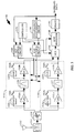
- FIG. 2 A block diagram of an exemplary receiver architecture of the present invention is shown in FIG. 2.
- the transmitted RF signal is received by antenna 1212, routed through duplexer 1214, and provided to attenuator 1216.
- Attenuator 1216 attenuates the RF signal to provide a signal at the required amplitude and provides the attenuated signal to RF processor 1210.
- the attenuated signal is provided to pad 1222a and low noise amplifier (LNA) 1220a.
- LNA 1220a amplifies the RF signal and provides the amplified signal to bandpass filter 1226.
- Pad 1222a provides a predetermined level of attenuation and connects in series with switch 1224a.
- Switch 1224a provides a bypass route around LNA 1220a when the gain of LNA 1220a is not needed.
- Bandpass filter 1226 filters the signal to remove spurious signals which can cause intermodulation products in the subsequent signal processing stages.
- the filtered signal is provided to pad 1222b and low noise amplifier (LNA) 1220b.
- LNA 1220b amplifies the filtered signal and provides the signal to RF/IF processor 1248.
- Pad 1222b provides a predetermined level of attenuation and connects in series with switch 1224b.
- Switch 1224b provides a bypass route around LNA 1220b when the gain of LNA 1220b is not needed.
- mixer 1230 downconverts the signal to an intermediate frequency (IF) with the sinusoidal from local oscillator (LO) 1228.
- IF intermediate frequency
- LO local oscillator
- the IF signal is provided to bandpass filter 1232 which filters out spurious signals and out-of-band downconversion products.
- the filtered IF signal is provided to voltage control amplifier (VGA) 1234 which amplifies the signal with a variable gain which is adjusted by a gain control signal.
- VGA voltage control amplifier
- Amplifier 1234 can also be implemented as a fixed gain amplifier, depending on the system requirement, and this is also within the scope of the present invention.
- the amplified IF signal is provided to demodulator 1250 which demodulates the signal in accordance with the modulation format used by the transmitter (not shown).
- RF processor 1210 and RF/IF processor 1248 is collectively referred to as a front end.
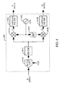
- FIG. 4 A block diagram of an exemplary demodulator 1250 used for demodulation of quadrature modulated signals (e.g. QPSK, OQPSK, and QAM) is illustrated in FIG. 4.
- demodulator 1250 is implemented as a subsampling bandpass demodulator.
- the IF signal is provided to bandpass sigma delta analog-to-digital converter ( ⁇ ADC) 1410 which quantizes the signal at a high sampling frequency determined by the CLK signal.
- ⁇ ADC bandpass sigma delta analog-to-digital converter
- An exemplary design of a ⁇ ADC is described in detail in U.S. Application Serial No. 08/928,874 entitled "SIGMA-DELTA ANALOG-TO-DIGITAL CONVERTER", filed September 12, 1997, and assigned to the assignee of the present invention.
- ⁇ ADC within a receiver is disclosed in copending U.S. Patent Application Serial No. 08/987,306, entitled "RECEIVER WITH SIGMA-DELTA ANALOG-TO-DIGITAL CONVERTER", filed December 9, 1997, assigned to the assignee of the present invention and incorporated by reference herein.
- the quantized signal is provided to filter 1412 which filters and decimates the signal.
- the filtered signal is provided to multipliers 1414a and 1414b which downconvert the signal to baseband with the in-phase and quadrature sinusoids from local oscillator (LO2) 1420 and phase shifter 1418, respectively.
- Phase shifter 1418 provides 90° of phase shift for the quadrature sinusoidal.
- the baseband I and Q signals are provided to lowpass filters 1416a and 1416b, respectively, which filter the signal to provide the I and Q data.
- the baseband data in FIG. 2 comprises the I and Q data in FIG. 4.
- filter 1412 and/or lowpass filters 1416 also provide scaling of the signal to enable demodulator 1250 to provide baseband data at various amplitudes.
- Other implementations of demodulator 1250 can be designed to performed the demodulation of QPSK modulated waveform and are within the scope of the present invention.
- receiver 1200 comprises the basic functionalities required by most receivers.
- the arrangement of attenuator 1216, LNAs 1220a and 1220b, bandpass filters 1226 and 1232, and mixer 1230 can be reordered to optimize the performance of receiver 1200 for specific applications.
- attenuator 1216 can be interposed between LNA 1220a and bandpass filter 1226 to improve the noise figure performance.
- a bandpass filter can be inserted before LNA 1220a to remove undesirable spurious signals before the first amplifier stage.
- Different arrangements of the functionalities shown herein can be contemplated and are within the scope of the present invention.
- other arrangements of the functionalities shown herein in combination with other receiver functionalities which are known in the art can also be contemplated and are within the scope of the present invention.
- Attenuator 1216, switches 1224a and 1224b, and demodulator 1250 are controlled by AGC control circuit 1260 such that the IF signal from amplifier 1234 is at the required amplitude.
- AGC control circuit 1260 is controlled by AGC control circuit 1260 such that the IF signal from amplifier 1234 is at the required amplitude.
- the AGC function is described in detail below.
- LNAs 1220a and 1220b are fixed gain amplifiers.
- LNAs 1220a and 1220b and mixer 1230 are controlled by bias control circuit 1280 to adjust the DC bias current and/or voltages of these active devices such that the required linearity performance is achieved with minimal power consumption.
- the variable IIP3 bias control mechanism is described in detail below.
- receiver architecture of the present invention can be adopted for use in various applications, including cellular telephone and HDTV applications.
- receiver 1200 can be adopted for use in CDMA communication systems operating at the personal communication system (PCS) band or the cellular band.
- PCS personal communication system
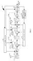
- FIG. 3 A block diagram of an exemplary receiver which supports dual-band (PCS and cellular) and dual-mode (CDMA and AMPS) is shown in FIG. 3.
- the PCS band has a bandwidth of 60 MHz and a center frequency of 1900 MHz.
- the cellular band has a bandwidth of 25 MHz and a center frequency of 900 MHz.
- Each band requires a unique RF bandpass filter. Therefore, two RF processors are used for the two bands.
- Receiver 1300 comprises many of the same components as those in receiver 1200 (see FIG. 2).
- Antenna 1312, duplexer 1314, and attenuator 1316 are identical to antenna 1212, duplexer 1214, and attenuator 1216 in receiver 1200.
- the attenuated signal from attenuator 1316 is provided to RF processors 1310a and 1310b.
- RF processor 1310a is designed to operate at the cellular band and RF processor 1310b is designed to operate at the PCS band.
- RF processor 1310a is identical to RF processor 1210 in receiver 1200.
- RF processor 1310a comprises two stages of low-noise amplifier (LNA) 1320a and 1320b connected in cascade with bandpass filter 1326 interposed between the stages.
- LNA low-noise amplifier
- Each LNA 1320 has a parallel signal path comprising pad 1322 and switch 1324.
- RF processor 1310b is similar to RF processor 1310a except that LNAs 1321a and 1321b and bandpass filter 1327 are designed to operate at the PCS band.
- the output from RF processors 1310a and 1310b are provided to multiplexer (MUX) 1346 which selects the desired signal in accordance with a control signal from controller 1370 (not shown in FIG. 3 for simplicity).
- the RF signal from MUX 1346 is provided to RF/IF processor 1348 which is identical to RF/IF processor 1248 in FIG. 2.
- the IF signal from processor 1348 is provided to demodulator (DEMOD) 1350 which demodulates the signal in accordance with the modulation format used at the remote transmitter (not shown).
- Demodulator 1350, AGC control circuit 1360, bias control circuit 1380, and non-linearity measurement circuit 1390 in FIG. 3 are identical to demodulator 1250, AGC control circuit 1260, bias control circuit 1280, and non-linearity measurement circuit 1290 in FIG. 2, respectively.
- Controller 1370 connects to AGC control circuit 1360, bias control circuit 1380, and MUX 1346 and controls the operation of these circuits.
- Controller 1370 can be implemented as a microprocessor, a microcontroller, or a digital signal processor programmed to perform the functions herein described.
- Controller 1370 can also comprise a memory storage element for storing the operating modes of receiver 1300 and the associated control signals.
- Attenuator 1216 has an attenuation range of 20 dB and provides an attenuation of 0.2 dB to -20 dB.
- Attenuator 1216 can be designed with a pair of diodes or by field effect transistors (FETs), the implementations of which are known in the art.
- FETs field effect transistors
- LNAs 1220a and 1220b have fixed gains of 13 dB each.
- LNAs 1220a and 1220b can be off-the-shelf monolithic RF amplifiers or amplifiers designed using discrete components.
- An exemplary discrete design of LNA 1220 is given in detail below.
- bandpass filter 1226 is a surface acoustic wave (SAW) filter which has a bandwidth of 25 MHz, the entire bandwidth of the cellular band, and is centered about 900 MHz.
- SAW surface acoustic wave
- bandpass filter 1232 is also a SAW filter which has a bandwidth of 1.2288 MHz, the bandwidth of one CDMA system, and is centered about 116.5 MHz.
- Mixer 1230 is an active mixer which can be an off-the-shelf mixer, such as the Motorola MC13143, or other active mixer which is designed in the manner known in the art. Mixer 1230 can also be implemented with passive components, such as double-balanced diode mixer.
- Amplifier 1234 can be a monolithic amplifier or an amplifier designed with discrete components. In the exemplary embodiment, amplifier 1234 is designed to provide a gain of 40 dB.
- the overall gain range of receiver 1200 is +51 dB to -5 dB.
- This gain range presumes exemplary insertion loss of -3 dB for bandpass filter 1226, gain of +1 dB for mixer 1230, and insertion loss of -13 dB for bandpass filter 1232.
- an AGC range of 80 dB is typically required to adequately handle path loss, fading conditions, and jammers.
- the AGC range provided by attenuator 1216, LNAs 1220a and 1220b, and pads 1222a and 1222b is 56 dB.
- the remaining 24 dB of AGC range is provided by demodulator 1250 and/or amplifier 1234.
- ADC 1410 quantizes the analog waveform and provides the digitized values to the subsequent digital signal processing blocks.
- the required resolution for ADC 1410 is four bits.
- an additional six bits of resolution provides headroom for the yet unfiltered jammers.
- ADC 1410 can be designed to provide more than ten bits of resolution. Each additional bit over ten can be used to provide 6 dB of gain control. Fortunately, at high CDMA signal levels, the out-of-band jammer levels cannot continue to be +72 dB above the CDMA signal.
- the jammers require less than 6 bits of resolution for jammer headroom.
- the AGC function performed in demodulator 1250 is active only when the CDMA signal is strong, e.g., at the high end of the CDMA control range.
- the extra bits of resolution which are initially reserved for jammer headroom are now used for the AGC function as the result of the strong CDMA signal levels.
- FIG. 5A A schematic diagram of an exemplary discrete LNA design is shown in FIG. 5A.
- the RF input is provided to one end of AC coupling capacitor 1512.
- the other end of capacitor 1512 connects to one end of capacitor 1514 and inductor 1516.
- the other end of capacitor 1514 connects to analog ground and the other end of inductor 1516 connects to one end of resistors 1518 and 1520 and the base of transistor 1540.
- the other end of resistor 1518 connects to the power supply Vdc and the other end of resistor 1520 connects to analog ground.
- Bypass capacitor 1522 connects to Vdc and analog ground.
- transistor 1540 is a low noise RF transistor, such as the Siemens BFP420, which is commonly used in the art.
- the emitter of transistor 1540 connects to one end of inductor 1542.
- the other end of inductor 1542 connects to current source 1580 which also connects to analog ground.
- the collector of transistor 1540 connects to one end of inductor 1532, resistor 1534, and capacitor 1536.
- the other end of inductor 1532 and resistor 1534 connect to Vdc.
- the other end of capacitor 1536 comprises the RF output.
- capacitors 1512 and 1536 provide AC coupling of the RF input and output signals, respectively.
- Capacitor 1514 and inductor 1516 provide noise matching.
- Inductors 1516 and 1532 also provide matching of the LNA input and output, respectively.
- Inductor 1532 also provides a DC path for the bias current of transistor 1540.
- Inductor 1542 provides degeneration of the emitter impedance to improve linearity.
- Resistors 1518 and 1520 set the DC bias voltage at the base of transistor 1540.
- Resistor 1534 determines the gain of LNA 1220 and the output impedance.
- Current source 1580 controls the bias current of transistor 1540 which determines the IIP3 of LNA 1220.
- FIG. 5B A schematic diagram of an exemplary current source 1580 is shown in FIG. 5B.
- the sources of n-channel MOSFETs 1582 and 1584 are connected to analog ground.
- the drain of MOSFET 1584 is connected to one end of resistor 1586.
- the other end of resistor 1586 connects to the drain of MOSFET 1582 and comprises the output of current source 1580.
- Bypass capacitor 1588 connects across the output of current source 1580 and analog ground.
- the gate of MOSFET 1582 is connected to Vbias1 and the gate of MOSFET 1584 is connected to Vbias2.
- MOSFETs 1582 and 1584 provide the collector bias current Icc for transistor 1540 which, in turn, determines the IIP3 operating point of LNA 1220.
- the gates of MOSFETs 1582 and 1584 are connected to a control voltages Vbias1 and Vbias2, respectively.
- Vbias1 low (e.g. 0V)
- MOSFET 1582 is turned OFF and provides no collector bias current Icc for transistor 1540.
- Vbias1 is high (e.g. approaching Vdc)
- MOSFET 1582 is turned ON and provides the maximum collector bias current for transistor 1540.
- Vbias1 determines the amount of collector bias current Icc provided by MOSFET 1582.
- Vbias2 determines the amount of collector bias current provided by MOSFET 1584.
- the voltage at the base of transistor 1540 and the value of resistor 1586 limit the maximum collector bias current provided by MOSFET 1584.
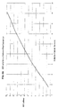
- the IIP3 performance of LNA 1220 versus collector bias current Icc is illustrated in FIG. 6A. Notice that the IIP3 increases approximately 6 dB per octave increase (or doubling) in collector bias current.
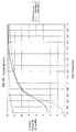
- the collector bias current of transistor 1540, the gain of LNA 1220, and the IIP3 of LNA 1220 versus the control voltage Vbias1 are illustrated in FIG. 6B. Notice that the gain is approximately constant (e.g. gain variation of approximately 1 dB for all Vbias1 voltages). Also, note that the IIP3 varies in similar manner with the collector bias current Icc. Thus, the collector bias current can be decreased, if high IIP3 is not required, with minimal effect on the gain of LNA 1220.
- FIGS. 5A and 5B illustrate an exemplary design of LNA 1220 and current source 1580, respectively.
- LNA 1220 can be designed using other topologies to provide the necessary performance (e.g. higher gain, improved noise figure, better matching).
- LNA 1220 can be designed with other active devices, such as bipolar-junction transistors (BJT), heterojunction-bipolar transistors (HBT), metal-oxide-semiconductor field effect transistor (MOSFET), gallium arsenide field effect transistor (GaAsFET), or other active devices.
- BJT bipolar-junction transistors
- HBT heterojunction-bipolar transistors
- MOSFET metal-oxide-semiconductor field effect transistor
- GaAsFET gallium arsenide field effect transistor
- LNA 1220 can also be implemented as monolithic amplifier in the manner known in the art.
- current source 1580 can be designed and implemented in other manners known in the art. The various implementations of LNA 1220
- in-band intermodulation products can be created by spurious signals passing through non-linear devices.
- One application which has a demanding linearity requirement is a CDMA communication system which is co-located with other cellular telephone systems, such as the Advance Mobile Phone System (AMPS).
- AMPS Advance Mobile Phone System
- the other cellular telephone systems can transmit spurious signals (or jammers) at high power near the operating band of the CDMA system, thereby necessitating high IIP3 requirement on the CDMA receiver.
- the spurious signal rejection requirement for a CDMA system is defined by two specifications, a two-tone test and a single-tone test, in the "TIA/EIA/IS-98-A Intermodulation Spurious Response Attenuation", hereinafter the IS-98-A standard.
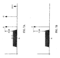
- the two-tone test is illustrated in FIG. 7A.
- the two tones are equal in amplitude and 58 dB higher than the amplitude of the CDMA signal.
- This test simulates an FM-modulated signal being transmitted on the adjacent channel, such as the signal from an AMPS system.
- the FM-modulated signal contains the bulk of the power in the carrier whereas the power in the CDMA waveform is spread across the 1.2288 MHz bandwidth.
- the CDMA signal is more immune to channel condition and is maintained at a low power level by a power control loop. In fact, the CDMA signal is maintained at the minimal power level necessary for a requisite level of performance to reduce interference and increase capacity.
- the single-tone test is illustrated in FIG. 7B.
- the linearity of the receiver is specified at the CDMA input power level of -101 dBm, -90 dBm, and -79 dBm.
- the jammers are at -43 dBm, -32 dBm, and -21 dBm (+58 dBc)
- the in-band equivalent signal of the intermodulation products are at -104 dBm, -93 dBm, and -82 dBm, for the input power level of -101 dBm, -90 dBm, and -79 dBm, respectively.
- the product at +2500 KHz can be easily filtered by the subsequent bandpass filters 1226 and 1232 (see FIG. 2).
- the product at +100 KHz falls within the CDMA waveform and degrades the CDMA signal.
- the IIP3 of the active devices within receiver 1200 is adjusted in accordance with the amount of non-linearity in the received signal.
- Receiver 1200 is designed to meet the two-tone intermodulation specification.
- the jammers are present for only a fraction of the operating time of receiver 1200.
- the amplitude of the jammers will rarely reach the +58 dB level as specified. Therefore, to design for the worse case jammers and to operate receiver 1200 in the high IIP3 mode in anticipation of the worse case jammers is a waste of battery power.
- the IIP3 of the active devices are adjusted in accordance with the measured non-linearity in the output signal from receiver 1200.
- the non-linearity is measured by the RSSI slope method.
- the measurement of the RSSI slope is described in detail in U.S. Patent No. 5,107,225, entitled “HIGH DYNAMIC RANGE CLOSED LOOP AUTOMATIC GAIN CONTROL CIRCUIT", issued April 21, 1992, assigned to the assignee of the present invention and incorporated by reference herein.
- bandpass filter 1232 has a bandwidth of 1.2288 MHz and suppresses most of the jammers and out-of-band intermodulation products.
- the IF signal from amplifier 1234 is provided to demodulator 1250 which processes the IF signal and provides the digitized baseband data which comprises the I and Q data.
- the baseband data is provided to non-linearity measurement circuit 1290.
- the power measurement is provided to bias control circuit 1280.
- the power measurement contains the power of the desired baseband I and Q signals as well as the power of the intermodulation products.
- the intermodulation products increase two dB for each dB increase in the input signal level.
- the intermodulation products increase three dB for each dB increase in the input signal level.
- the amount of intermodulation can be estimated by measurement of the RSSI slope which is defined as the change in the output signal level versus the change in the input signal level.
- the change in the input signal level can be set at a predetermined increment (e.g. 0.5 dB).
- 0.5 dB increase in the input signal level corresponds to 0.5 dB increase in the output signal level and an RSSI slope of 1.0.
- the RSSI slope increases as one or more active devices transitions into the non-linear operating region.
- a higher RSSI slope corresponds to greater level of non-linearity.
- An RSSI slope of 3.0 corresponds to receiver 1200 operating in total compression (e.g. no increase in the desired output signal level as the input is increased) and the output being dominated by third order intermodulation products.
- the RSSI slope can be compared against a predetermined RSSI threshold. If the RSSI slope exceeds the threshold, the IIP3 of the proper active device is increased. Alternatively, if the RSSI slope is below the RSSI threshold, the IIP3 is decreased.
- the RSSI threshold can be adjusted during operation of receiver 1200 based on the required bit-error-rate (BER) or frame-error-rate (FER) performance. A higher RSSI threshold allows for higher level of intermodulation products before increasing the IIP3, thereby minimizing power consumption at the expense of BER or FER performance.
- the RSSI threshold can also be adjusted by a control loop which sets the threshold for a required level of performance (e.g. 1% FER). In the exemplary embodiment, the RSSI slope is selected to be 1.2. However, the use of other RSSI thresholds are within the scope of the present invention.
- the RSSI slope is one method for measuring the level of non-linearity.
- the level of non-linearity can also be measured by calculating the change in the energy-per-chip-to-noise-ratio (Ec/Io) of the output signal for an incremental change in the amplitude of the input signal.
- the intermodulation products increase by a factor of three to one when receiver 1200 is in compression and the output signal is dominated by third order intermodulation products.
- the level of non-linearity can be estimated by the change in Ec/Io versus the change in the input signal level.
- Other methods to measure the level of non-linearity can be contemplated and are within the scope of the present invention.
- the IIP3 of the active devices are adjusted in a accordance with the amount of non-linearity (e.g. through measurement of the RSSI slope) experienced by each active device.
- LNAs 1220a and 1220b provide a fixed gain.
- mixer 1230 experiences the largest signal level
- LNA 1220b experiences the next largest signal level
- LNA 1220a experiences the smallest signal level (this presumes that the gain of LNA 1220a is larger than the insertion loss of bandpass filter 1226).
- the IIP3 operating point of mixer 1230 is increased first if a jammer is detected (e.g. through high RSSI slope measurement). Once the IIP3 of mixer 1230 is fully adjusted (e.g.
- the IIP3 of LNA 1220b is increased.
- the IIP3 of LNA 1220a can be increased.
- LNA 1220a is maintained at a predetermined IIP3 operating point to optimize the performance of receiver 1200 .
- the IIP3 of LNA 1220b is decreased first if no jammer is detected. Once the IIP3 of LNA 1220b is fully adjusted (e.g. to the lowest IIP3 operating point), the IIP3 of mixer 1230 is decreased.
- the IIP3 of LNA 1220b and mixer 1230 can be adjusted in continuous manner (e.g. by providing for continuous Vbias1 and Vbias2 control voltages) or in discrete steps.
- the present invention is directed to the use of continuous, discrete steps, or other methods for controlling the IIP3 of the active devices.
- IIP3 adjustment presumes that IIP3 is the only consideration. However, different applications may experience different input conditions and have different performance requirements. The order of IIP3 adjustment can be rearranged to meet these requirements. Furthermore, the IIP3 adjustment can be reversed in direction from that described above (e.g. decreasing IIP3 for increasing input signal level) to optimize the performance of receiver 1200 for a particular operating condition. Different order of IIP3 adjustment and different direction of IIP3 adjustment are within the scope of the present invention.
- the required AGC range is nominally 80 dB.
- the AGC range is provided by attenuator 1216, LNAs 1220a and 1220b, pads 1222a and 1222b, demodulator 1250, and possibly amplifier 1234.
- attenuator 1216 provides an AGC range of 20 dB
- pad 1222a and 1222b each provide an AGC range of 5 dB
- LNA 1220a and 1220b each provide an AGC range of 13 dB
- amplifier 1234 and/or demodulator 1250 provides an AGC range of 24 dB.
- amplifier 1234 can be designed to provide an AGC range to supplements those of other components.
- the AGC range of pads 1222 can be reduced to 2 dB each and amplifier 1234 can be designed with 6 dB of AGC range.
- the first 2 dB of AGC range is provided by demodulator 1250.
- Demodulator 1250 comprises bandpass subsampling ⁇ ADC 1410 which provides additional bits of resolution which can be used for AGC control.
- the next 20 dB of AGC range is provided by attenuator 1216 and/or amplifier 1234.
- the next 18 dB of AGC range is provided by LNAs 1220a and pad 1222a.
- the next 18 dB of AGC range is provided by LNAs 1220b and pad 1222b.
- the remaining 22 dB of AGC range is provided by amplifier 1234 and/or demodulator 1250.
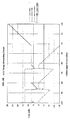
- FIG. 8A An exemplary diagram illustrating the AGC control operation of receiver 1200 of the present invention for ascending CDMA input signal power is illustrated in FIG. 8A.
- amplifier 1234 is implemented as a fixed gain amplifier for simplicity.
- the CDMA input power level can range from -104 dBm to -24 dBm. From -104 dBm to -102 dBm, LNAs 1220a and 1220b are turned ON, switches 1224a and 1224b are switched OFF, and the AGC is provided by demodulator 1250. From -102 dBm to -85 dBm the AGC is provided by attenuator 1216.
- LNA 1220a is turned OFF, switch 1224a is switched ON, LNA 1220b remains ON, switch 1224b remains OFF, and the AGC is provided by attenuator 1216.
- LNAs 1220a and 1220b are turned OFF, switches 1224a and 1224b are switched ON, and the AGC is provided by attenuator 1216.
- attenuator 1216 is fully attenuated, the IF signal level into demodulator 1250 increases dB per dB with the input RF signal level, and the AGC is provided after ADC 1410 by demodulator 1250.
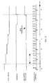
- FIG. 8B An exemplary diagram illustrating the AGC control operation of receiver 1200 for descending CDMA signal power is illustrated in FIG. 8B.
- amplifier 1234 is implemented as a fixed gain amplifier in this example for simplicity.
- LNAs 1220a and 1220b are turned OFF, switches 1224a and 1224b are switched ON, and the AGC is provided after ADC 1410 by demodulator 1250.
- the AGC is provided by attenuator 1216.
- Attenuator 1216 is at the minimum attenuation state and the AGC is provided by demodulator 1250.
- LNA 1220b is turned ON and switch 1224b is switched OFF.
- the AGC is provided by attenuator 1216.
- the AGC is provided by demodulator 1250.
- LNA 1220a is turned ON and switch 1224a is switched OFF.
- the AGC is provided by attenuator 1216.
- the AGC is provided by demodulator 1250.
- FIGS. 8A-8B illustrate the input RF signal levels where LNAs 1220a and 1220b are turned ON and OFF.
- LNA 1220a is turned OFF as the input signal level exceeds -85 dBm (see FIG. 8A) but is not turned ON again until the signal level decreases past -91 dBm.
- the 6 dB of hysteresis prevents LNA 1220a from toggling between the ON and OFF states.
- LNA 1220b also is provided with 6 dB of hysteresis for the same reason. Different amounts of hysteresis can be used to optimize system performance and are within the scope of the present invention.
- the discussion above illustrates an exemplary implementation of the required AGC control.
- the AGC control can also be implemented with AGC amplifiers having adjustable gains.
- the arrangement of attenuator 1216 and LNAs 1220a and 1220b as illustrated in FIG. 2 is just one implementation which satisfies the CDMA specification.
- Other implementations of the AGC functionalities using the elements described herein, and other implementations using these elements in combination with other elements or circuits which are known in the art, are within the scope of the present invention.
- the IIP3 of the active devices are set in accordance with the measured level of non-linearity produced by receiver 1200.
- the level of non-linearity can be estimated by the RSSI slope or by Ec/Io measurement.
- the timing diagram of an exemplary RSSI slope measurement implementation is illustrated in FIG. 9.
- the input RF signal level is changed by varying the attenuation of attenuator 1216 in narrow pulses. Each pulse is referred to as a "wiggle".
- the RSSI slope is measured for each pulse and the measurements are averaged over a predetermined period T to improve the accuracy of the RSSI slope measurement. At the end of the period T, the measured RSSI slope is compared to the RSSI threshold and the result is used to adjust the IIP3 of the active devices in the manner described above.
- the RSSI slope measurement at T 0 is less than the RSSI threshold, indicating that receiver 1200 is operating within the linear limit.
- the IIP3 of LNA 1220b is decreased to conserve power consumption.
- the measured RSSI slope is less than the RSSI threshold and the IIP3 of LNA 1220b continues to be decreased.
- the measured RSSI slope is still less than the RSSI threshold and the IIP3 of mixer 1230 is decreased since the IIP3 of LNA 1220b has been adjusted fully to the minimal IIP3 operating point.
- the measured RSSI slope is greater than the RSSI threshold, indicating that the intermodulation products has increased to an unacceptable level.
- the IIP3 of mixer 1230 is increased to improve linearity in response thereto.
- each pulse is 200 ⁇ sec in duration
- the period T is 5 msec
- the number of pulses within one period T is nine.
- the duty cycle is 36 percent.
- the duty cycle of the pulses should be low enough so that the Ec/Io of the desired signal is minimally degraded by the periodic perturbation in the signal amplitude.
- the width of the pulses is selected to be short in duration to minimize disturbance to AGC control circuit 1280.
- the AGC control loop is slow and cannot track the changes in signal level caused by the short attenuation pulses.
- the present invention is directed at the use of pulses of various widths and various duty cycles for the functions described herein.
- the amplitude of the perturbation in the input RF signal level is selected to be small to minimize degradation in the output signal and to minimize effect on the IIP3 of the entire receiver 1200.
- the attenuation step for RSSI slope measurement is 0.5 dB. Other values for the attenuation step can be used and are within the scope of the present invention.
- the RSSI threshold is selected to be 1.2.
- the use of one RSSI threshold can result in toggling the IIP3 operating points between successive periods T.
- two RSSI thresholds can be used to provide hysteresis.
- the IIP3 is not increased unless the measured RSSI slope exceeds the first RSSI threshold and the IIP3 is not decreased unless the measured RSSI slope is below the second RSSI threshold.
- the use of a single threshold or multiple thresholds are within the scope of the present invention.
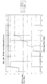
- FIG. 10A A diagram illustrating the IIP3 bias control operation of receiver 1200 of the present invention for ascending input RF power level is shown in FIG. 10A.
- the input RF signal comprises a CDMA signal and two-tone jammers which are +58 dBc above the CDMA signal.
- the CDMA signal power is between -104 dBm and -101 dBm
- the IIP3 of mixer 1230 is set at +10 dBm and the IIP3 of LNAs 1220a and 1220b are set at 0 dBm.
- the measured RSSI slope exceeds the RSSI threshold, and the IIP3 of mixer 1230 is increased to +15 dBm to minimize the level of non-linearity.
- Attenuator 1216 provides attenuation of the input RF signal between -104 dBm and -84dBm.
- LNA 1220a is bypassed and attenuator 1216 resets to its low attenuation state.
- the CDMA signal power is at -83 dBm, -79 dBm, -75 dBm, and -71 dBm, the IIP3 of LNA 1220b is increased to minimize intermodulation products.
- LNA 1220b is bypassed and attenuator 1216 again resets to its low attenuation state.
- FIG. 10B A diagram illustrating the IIP3 bias control operation of receiver 1200 for descending input RF power level is shown in FIG. 10B.
- the input RF signal comprises a CDMA signal and two-tone jammers which are +58 dBc above the CDMA signal.
- LNAs 1220a and 1220b are bypassed.
- LNA 1220b is turned ON to provide the necessary gain.
- the IIP3 of LNA 1220b is decreased to minimize power consumption.
- the input RF power level where the IIP3 of mixer 1230 and LNAs 1220a and 1220b are adjusted are determined by the measured RSSI slope.
- the RSSI slope measurement may not result in linearly spaced IIP3 bias switch points as shown in FIGS. 10A and 10B.
- the stepwise switch points can be replaced with continuously adjustable bias control.
- the IIP3 of the active devices are set in accordance with the operating mode of the receiver.
- receiver 1300 can be used in a cellular telephone which is required to operate in either PCS or cellular band.
- Each band can support either digital and/or analog platforms.
- Each platform can further comprise a variety of operating modes. The various operating modes are utilized to improve performance and conserve battery power.
- different operating modes are used to support the following features of a cellular telephone : (1) slotted mode paging for longer stand-by time, (2) gain step for dynamic range enhancement, (3) punctured transmitter output for longer talk time, (4) frequency band selection for dual-band phones (PCS and cellular), (5) multiple access toggling between systems (CDMA, AMPS, GSM, etc.), and (6) means for circuit bias control in the presence of jammers.
- the operating modes of the cellular telephone can have different performance requirements.
- each operating mode is assigned a unique identifier comprising N mode bits.
- the mode bits define particular characteristics of the operating mode. For example, one mode bit can be used to select between the PCS and cellular band and another mode bit can be used to select between digital (CDMA) or analog (FM) mode.
- the N mode bits are provided to a logic circuitry within controller 1370 which decodes the N mode bits into a control bus comprising up to 2 N control bits.
- the control bus is routed to circuits within receiver 1300 which require control.
- control bus can direct the following : (1) set the IIP3 of the mixer within RF/IF processor 1348 and the LNAs within RF processors 1310a and 1310b, (2) set the gain of receiver 1300, (3) set the DC bias voltages and/or current to other RF and IF circuitry within receiver 1300, (4) select the desired signal band, and (5) set the oscillators to the proper frequencies.
- Receiver 1300 supports dual-band (PCS and cellular) and dual-mode (CDMA and FM).
- PCS dual-band
- CDMA dual-mode
- FM both CDMA and FM transmissions
- four mode bits are utilized.
- the four mode bits are the BAND_SELECT, IDLE/, FM/, and LNA_RANGE bits.
- receiver 1300 When BAND_SELECT is set to 0 (cellular band), receiver 1300 operates in one of the cellular operating modes listed in Table 1. Table 1 only lists the IIP3 operating point of LNAs 1320a and 1320b. A similar table can be generated for the IIP3 operating point of the active mixer within RF/IF processor 1348. While in the cellular mode, the DC bias current for LNAs 1321a and 1321b are turned OFF to conserve battery power.
- Tables 1 and 2 list the IIP3 operating points of the LNAs to minimize power consumption while maintaining the require performance. Additional tables can be generated for other circuits which require control. For example, a table can be generated which sets the AGC to the proper operating range based on the expected input signal level for the desired operating mode. Other tables can be generated to set the DC bias voltages or current which are required by various circuits within receiver 1300.
- the IIP3 of the active devices are set in accordance with the measured amplitude of the signal at various signal processing stages within the receiver.
- power detectors can be connected to the output of selected components to measure the power level of the signal.
- power detectors can be connected to the output of LNA 1220a and 1220b and mixer 1230 to measure the power of the RF signal from these components.
- the power measurements are then provided to bias control circuit 1280 which use the information to adjust the IIP3 operating point of any component operating past a predetermined level of non-linearity.
- power detectors can be connected to the output of mixer 1230 and demodulator 1250 to measure the power of the RF signal and baseband signal, respectively, from these components.
- the power measurements are also provided to bias control circuit 1280.
- the difference in power between these two measurements represents the power from the out-of-band signals, which can be used to infer the required IIP3 performance.
- Bias control circuit 1280 adjusts the operating point of the components in the manner described above to maintain the required level of performance.
- the power detector can be implemented in many manner known in the art, such was a diode detector follow by a lowpass filter.
- the ⁇ ADC within the receiver of the present invention can be designed to provide the required dynamic range while minimizing power consumption. Power consumption is especially important in CDMA communication systems because of the portable nature of the cellular telephone.
- the ⁇ ADC can be designed to minimize power consumption by providing for sections of the ⁇ ADC to be disabled when high dynamic range is not required.
- the ⁇ ADC can also be designed with adjustable bias current which can be varied based on the amplitude of the signal into the ⁇ ADC and the required performance.
- the reference voltage of the ⁇ ADC can also be adjusted lower when less dynamic range is required to minimize power consumption.
- the sampling frequency of the ⁇ ADC can also be lowered when high dynamic range is not required to further minimize power consumption.
- the receiver is designed to operate under various operating conditions as specified by the IS-98-A standard.
- the input RF signal comprises a CDMA signal which ranges from -104 dBm to -79 dBm.
- IS-98-A specifies a two-tone and a single-tone operating condition.
- the input RF signal comprises the CDMA signal and two jammers which are each +58 dBc above the amplitude of the CDMA signal and are located +900KHz and +1700KHz from the center frequency of the CDMA signal.
- the input RF signal comprises the CDMA signal and a signal jammer which is +72 dBc above the amplitude of the CDMA signal and is located +900KHz from the center frequency of the CDMA signal.
- the ⁇ ADC is designed with the necessary dynamic range to operate under the worse case operating conditions. In practice, these worse case conditions occur infrequently. Therefore, operating the ⁇ ADC in the high dynamic range mode at all times represents a waste of resource.
- the ⁇ ADC can be configured to minimize power consumption when high dynamic range is not required.
- the amplitude of the desired signal (e.g. the in-band CDMA signal) into the ⁇ ADC is maintained at +20 dB above the noise floor of the ⁇ ADC. This can be accomplished by measuring the amplitude of the desired signal after the digital signal processing and using the measured amplitude to adjust the gains of the front end.
- the above condition e.g. +18 dB above the noise floor
- a ⁇ ADC with four bits of resolution can be utilized to quantize the desired signal.
- the signal into the ⁇ ADC comprises the desired signal plus jammers.
- the amplitude of the jammers can vary over a wide range and can make up a significant portion of the signal into the ⁇ ADC.
- the desired signal and jammers need to fall within the ceiling of the ⁇ ADC so that clipping of these signals do not occur.
- the jammers need to be properly quantized by the ⁇ ADC (even though the jammers are eventually filtered out by the subsequent digital signal processing) since clipping of the jammers results in intermodulation products which may fall into the signal band and degrade the desired signal.
- the ⁇ ADC is designed to provide 12 bits of resolution to meet the worse case operating conditions. The remaining eight bits of resolution are reserved for jammers and AGC control. The dynamic range of the ⁇ ADC can be adjusted such that the desired signal and the jammers are properly quantized, without clipping, while minimizing power consumption.
- the required dynamic range can be estimated by measuring the amplitude of the desire signal and the amplitude of the signal into the ⁇ ADC.
- the amplitude of the desired signal can be measured by computing the RSSI of the desired signal.
- the RSSI measurement is described in detail in the aforementioned U.S. Patent No. 5,107,225.
- the RSSI measurement is performed on the desired signal after the digital signal processing which removes undesirable images and spurious signals.
- the amplitude of the signal into the ⁇ ADC can be measured by a power detector connected to the input of the ⁇ ADC.
- the power detector can be implemented in the manner known in the art, such as an envelop detector implemented with a diode or a peak detector.
- the peak detector can detect if the input signal into the ⁇ ADC is above the saturating voltage of the ⁇ ADC which is half of the reference voltage. When this occurs, the ⁇ ADC can be switched to a higher dynamic range mode.
- the amplitude of the signal into ⁇ ADC can be estimated from measurement of the amplitude of the signal from various components within the front end, such as the output of mixer 1230 or the output of bandpass filter 1234 (see FIG. 2).
- a power detector can be used to measure the amplitude of the signal.
- the gain of the components interposed between the power detector and the ⁇ ADC is taken into account in calculating the amplitude of the signal into the ⁇ ADC.
- the spectral content of the measured signal should approximate the spectral content of the signal into the ⁇ ADC to enhance the accuracy of the estimate. Inaccuracy in the estimate results in a non-optimal dynamic range adjustment mechanism.
- the required dynamic range can be determined based on the operating mode of the receiver.
- Each operating mode can be associated with a different operating condition. For example, CDMA mode requires high dynamic range because of possible jammers near the signal band. FM mode requires less dynamic range since the input requirements are less stringent.
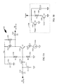
- loop 110a provides a first dynamic range and has a low noise floor.
- Loop 110b provides a second dynamic range but has a slightly higher noise floor than loop 110a.
- the lower noise floor of loop 110a is partially the result of biasing the amplifiers within loop 110a with higher bias current and using larger capacitors with loop 110a.
- each loop 110 within MASH ADC 100 can be selectively disabled, based on the amplitude of the signal into the ⁇ ADC and the required dynamic range, to minimize power consumption.
- the bias current of the amplifiers within each loop 110 can be adjusted to minimize power consumption and maintain the required performance.
- the signal into the ⁇ ADC is provided to loop 110a, the bias current of all amplifiers is set high, and MASH ADC 100 operates in the manner described above.
- This operating condition may result from an input RF signal comprising the CDMA signal and two large jammers at +58 dBc or an input RF signal comprising the CDMA signal and one large jammer at +72 dBc.
- loop 110b can be disabled and the output Y1 from loop 110a comprises the output from the ⁇ ADC.
- loop 110a can be disabled, the signal into the ⁇ ADC can be provided to loop 110b, and the output Y2 from loop 110b comprises the output from the ⁇ ADC.
- one to two loops can be enabled to provide the required dynamic range.
- the dynamic range thresholds wherein the loops are disabled can be selected based on numerous considerations.
- the thresholds can be selected based on the statistics of the amplitude of the input RF signal. For example, the percentage of time the input RF signal comprises jammers of various amplitudes can be tabulated. This information can be used to select the dynamic range thresholds which yield the minimum power consumption by ensuring that the minimal number of loop is enabled most of the time.
- the thresholds can also be selected based on the design performance of the ⁇ ADC.
- each threshold can be implemented with hysteresis to prevent toggling of the loops between the enabled and disabled states. An exemplary implementation of hysteresis is described below.
- the bias current of the amplifiers in each loop 110 can be adjusted to minimize power consumption while providing the required performance.
- loop 110a is designed to consume a maximum of 10 mA of bias current and loop 110b is designed to consume a maximum of 6 mA of bias current.
- the amplifier within resonator 130a is designed to consume 6 mA and the amplifier within resonator 130b is designed to consume 4 mA.
- the bias current for each amplifier is set high.
- the bias current can be decreased. Dynamic range varies approximately proportional to the bias current such that a two-fold decrease in bias current results in 6 dB less of dynamic range.
- the bias current of the amplifier within resonator 130a can be decreased from 6 mA down to 3 mA and the bias current of the amplifier within resonator 130b can be decreased from 4 mA down to 2 mA when 6 dB less of dynamic range is required.
- the bias current for the amplifiers within loop 110b can be decreased accordingly when high dynamic range is not required.
- the bias current can be adjusted in discrete steps or in a continuous manner.
- An additional mechanism to minimize power consumption is through adjustment of the reference voltage within the ⁇ ADC.
- the dynamic range of the ⁇ ADC is determined by the maximum input signal swing and the noise from ⁇ ADC which comprises the circuit noise and the quantization noise. As the required dynamic range decreases, the reference voltage can be lowered while maintaining approximately the same noise level. This is especially true when one loop is switched out and the quantization noise increases such that it is much greater than the circuit noise because the reference voltage of the ⁇ ADC is maintained constant. By lowering the reference voltage such that the quantization noise is approximately equal to the circuit noise, the desired level of performance is provided while maintaining the signal level at a low level. By decreasing the reference voltage and the signal swing within the ⁇ ADC, the amplifier bias current can be decreased. As an additional benefit, the amplifier driving the ⁇ ADC has a lower maximum signal swing and can also be biased with less current.
- Adjustment of the amplifier bias current can be performed independently of the disablement of the loops, or can be performed in conjunction with the disablement of the loops.
- the loops are enabled based on a coarse range of required dynamic range and the bias current are used for fine adjustment of dynamic range.
- analysis and measurements can be performed to determine the dynamic range provided by various configurations of the ⁇ ADC. This information can be tabulated and stored. Then, based on the required dynamic range, the ⁇ ADC can be configured accordingly, using the tabulated data.
- the various methods used to configure the ⁇ ADC to provide the required dynamic range while minimizing power consumption are within the scope of the present invention.
- the ⁇ ADC provides 79 dB of dynamic range (or greater than 12 bits of resolution) when both loops are enabled and an oversampling ratio (OSR) of 32 is utilized.
- OSR oversampling ratio
- loop 110a provides 54 dB of dynamic range
- loop 110b provides 42 dB of dynamic range
- loops 110a and 110b provide 79 dB of dynamic range when combined.
- a margin of 6 dB is reserved to handle fluctuations in the amplitude of the input RF signal.
- each dynamic range threshold can be implemented with hysteresis to prevent toggling between the enabled and disabled states.
- each dynamic range threshold comprises an upper threshold and a lower threshold.
- the loop with the higher dynamic range is not enabled unless the required dynamic range exceeds the upper threshold and the loop with the lower dynamic range is not enabled unless the required dynamic range falls below the lower threshold.
- loop 110a is not enabled unless the required dynamic range exceeds 51 dB. While operating with only loop 110a, loop 110b is enabled and loop 110a is disabled only if the required dynamic range falls below 45 dB.
- An exemplary application of the present invention for a CDMA communication system is tabulated in Table 3.
- the desired signal level is high, low dynamic range is required and only loop 110b is enabled.
- the desired signal level is low and the jammer level is high, high dynamic range is required to properly quantize the jammer and desired signal.
- the desired signal level is low and the jammer level is low, two options are available.
- the signal into the ⁇ ADC can be amplified, increasing the low signal level into a high signal level which can be sampled by loop 110b.
- loop 110a can be used to sample the signal but the bias current can be decreased to conserve power and the DAC level within loop 110a can be decreased to match the low signal level.
- Table 3 ADC Configuration Based on Input Signal Signal Level Jammer Level ADC Configuration low low enable loop 110b or loop 110b 1 low high enable loop 110a and loop 110b high low enable loop 110b high high enable loop 110b Note 1: 1) first option is to enable loop 110b and amplify the signal into the ⁇ ADC by 6 dB; 2) second option is to enable loop 110a and decrease the bias current and DAC level in loop 110a
- the dynamic range of the ⁇ ADC is a function of the oversampling ratio.
- Higher sampling frequency corresponds to higher oversampling ratio, since the bandwidth of the input signal is fixed, and higher dynamic range.
- higher sampling frequency can result in higher power consumption by the circuits which are used to implement the ⁇ ADC.
- the power consumption of CMOS circuits is proportional to the frequency of the switching clocks of the CMOS circuits.
- higher operating frequency requires wider bandwidth circuits which typically require more bias current.
- Higher switching frequency requires more bias current in the switches and more bias current in the amplifiers for faster settling .
- the sampling frequency of the ⁇ ADC can be decreased to minimize power consumption when high dynamic range is not required. Decreasing the sampling frequency allows the circuits within the ⁇ ADC to be biased with less current. Also, lower sampling frequency can result in less power dissipation in the circuits within the ⁇ ADC.
- oversampling ratio for oversampling ratio of less than 16, dynamic range decreases faster than 27 dB/octave.
- the oversampling ratio is maintained at a minimum of 16.
- the center frequency of the IF signal (e. g. the signal into the ⁇ ADC) is dependent on the sampling frequency.
- the first frequency downconversion is adjusted to produce an IF signal at the new IF frequency which is necessitated by the new sampling frequency. Care should be exercised such that spurious signals and harmonics of excessive amplitude do not fall in the new IF band.
- the receiver can also be designed with two or more ⁇ ADCs to support two or more operating modes. This allows each ⁇ ADC to be optimize to provide the required performance while minimizing power consumption.
- the appropriate ⁇ ADC can be switched on depending on the operating mode. For example, a receiver can be designed with two ⁇ ADCs, one for CDMA mode and one for FM mode. The ⁇ ADC for the FM mode can be designed to consume significantly less power because of the lower signal bandwidth and the lower required dynamic range. The appropriate ⁇ ADC can be switched on depending on whether the receiver is operating in the CDMA or FM mode.
Claims (22)
- Ein Empfänger mit programmierbarem dynamischem Bereich (1200), der Folgendes aufweist:ein Frontend (1210, 1248) zum Empfangen eines HF-Signals und zum Erzeugen eines Zwischenfrequenz- bzw. ZF-Signals (IF = intermediate frequency);einen ΣΔ-ADC (1410) verbunden mit dem HF-Prozessor (1210) zum Empfangen des ZF-Signals und zum Erzeugen von ZF-Abtastungen, wobei der ΣΔ-ADC einen dynamischen Bereich besitzt;einen Leistungsdetektor verbunden mit dem HF-Prozessor (1210) zum Messen einer Amplitude des ZF-Signals; undeinen Digitalsignalprozessor (1370) verbunden mit dem ΣΔ-ADC zum Empfangen der ZF-Abtastungen und zum Erzeugen eines gewünschten Signals;gekennzeichnet dadurch, dass der dynamische Bereich des ΣΔ-ADCs angepasst ist basierend auf einem benötigten dynamischen Bereich, wobei der benötigte dynamische Bereich abhängig ist von der Amplitude des ZF-Signals.
- Empfänger nach Anspruch 1, wobei der ΣΔ-ADC mehrere Schleifen bzw. Loops (110) aufweist, wobei jede Schleife aktiviert oder gesperrt wird in Abhängigkeit von dem benötigten dynamischen Bereich.
- Empfänger nach Anspruch 2, wobei der ΣΔ-ADC ein MASH 4-4 ADC ist, wobei der MASH 4-4 ADC eine erste Schleife und eine zweite Schleife aufweist.
- Empfänger nach Anspruch 3, wobei die erste Schleife von MASH 4-4 ADC verwendet wird, wenn der benötigte dynamische Bereich geringer ist als eine erste Dynamikbereichsschwelle, wobei die zweite Schleife verwendet wird, wenn der benötigte dynamische Bereich über der ersten Dynamikbereichsschwelle liegt und geringer ist als eine zweite Dynamikbereichsschwelle, und wobei die erste Schleife und die zweite Schleife verwendet werden, wenn der benötigte dynamische Bereich über der zweiten Dynamikbereichsschwelle liegt.
- Empfänger nach Anspruch 4, wobei die ersten und zweiten Dynamikbereichsschwellen mit Hysterese implementiert sind.
- Empfänger nach Anspruch 1, wobei der ΣΔ-ADC Verstärker (1220) aufweist, wobei die Verstärker einen Bias- bzw. Vorspannstrom besitzen.
- Empfänger nach Anspruch 6, wobei der Bias-Strom der Verstärker angepasst wird, basierend auf dem benötigten dynamischen Bereich.
- Ein Verfahren zum Vorsehen eines programmierbaren dynamischen Bereichs in einem Empfänger (1200), wobei das Verfahren folgende Schritte aufweist:Empfangen eines HF-Signals;Verarbeiten des HF-Signals, um ein ZF-Signal zu erzeugen;Abtasten des ZF-Signals mit einem ΣΔ-ADC (1410), um ZF-Abtastungen zu erzeugen, wobei der ΣΔ-ADC einen dynamischen Bereich besitzt;Verarbeiten der ZF-Abtastungen, um ein gewünschtes Signal zu erzeugen;dadurch gekennzeichnet, dass das Verfahren die weiteren folgenden Schritte aufweist:Messen einer Amplitude des ZF-Signals;Messen einer Amplitude des gewünschten Signals;Berechnen eines gewünschten dynamischen Bereichs gemäß der gemessenen Amplitude des ZF-Signals und der gemessenen Amplitude des gewünschten Signals; undAnpassen des dynamischen Bereichs des ΣΔ-ADCs gemäß dem benötigten dynamischen Bereich.
- Verfahren nach Anspruch 8, wobei der Anpassungsschritt folgenden Schritte aufweist:Aktivieren einer ersten Schleife innerhalb des ΣΔ-ADCs, wenn der benötigte dynamische Bereich unter einer ersten Dynamikbereichschwelle liegt.
- Verfahren nach Anspruch 9, wobei der Anpassungsschritt weiterhin folgenden Schritt aufweist:Aktivieren einer zweiten Schleife innerhalb des ΣΔ-ADCs, wenn der benötigte dynamische Bereich über der ersten Dynamikbereichsschwelle liegt und unter einer zweiten Dynamikbereichsschwelle liegt.
- Verfahren nach Anspruch 10, wobei der Anpassungsschritt weiterhin folgenden Schritt aufweist:Aktivieren der ersten Schleife innerhalb des ΣΔ-ADCs, wenn der benötigte dynamische Bereich über der zweiten Dynamikbereichsschwelle liegt.
- Verfahren nach Anspruch 11, wobei die ersten und zweiten Dynamikbereichsschwellen mit Hysterese implementiert sind.
- Verfahren nach Anspruch 11, wobei die ersten und zweiten Dynamikbereichsschwellen ausgewählt werden basierend auf Statistiken des HF-Signals.
- Verfahren nach Anspruch 11, wobei die ersten und zweiten Dynamikbereichsschwellen ausgewählt werden basierend auf einer Performance des ΣΔ-ADCs.
- Verfahren nach Anspruch 8, wobei der Anpassungsschritt folgenden Schritt aufweist:Anpassen eines Bias-Stromes des ΣΔ-ADCs basierend auf dem benötigten dynamischen Bereich.
- Verfahren nach Anspruch 8, wobei der Anpassungsschritt folgenden Schritt aufweist:Verändern einer Abtastfrequenz des ΣΔ-ADCs basierend auf dem benötigten dynamischen Bereich.
- Verfahren nach Anspruch 16, wobei der Anpassungsschritt weiterhin folgenden Schritt aufweist:Halten eines Oversampling-Verhältnisses des ΣΔ-ADCs auf einem Minimum von 16.
- Verfahren nach Anspruch 8, wobei das HF-Signal ein CDMA-Signal aufweist.
- Verfahren nach Anspruch 18, wobei der ΣΔ-ADC mehr als vier Bits Auflösung besitzt.
- Verfahren nach Anspruch 19, das weiterhin folgenden Schritt aufweist:Halten des gewünschten Signals auf 18 dB über einem Rauschboden bzw. Grund des ΣΔ-ADCs.
- Verfahren nach Anspruch 20, wobei der benötigte dynamische Bereich berechnet wird, so dass das ZF-Signal nicht durch den ΣΔ-ADC abgeschnitten ist.
- Verfahren nach Anspruch 1, wobei der benötigte dynamische Bereich weiter abhängig ist von der Amplitude des gewünschten Signals.
Applications Claiming Priority (3)
| Application Number | Priority Date | Filing Date | Title |
|---|---|---|---|
| US08/987,853 US6134430A (en) | 1997-12-09 | 1997-12-09 | Programmable dynamic range receiver with adjustable dynamic range analog to digital converter |
| US987853 | 1997-12-09 | ||
| PCT/US1998/026053 WO1999030427A1 (en) | 1997-12-09 | 1998-12-08 | Programmable dynamic range receiver |
Publications (2)
| Publication Number | Publication Date |
|---|---|
| EP1038360A1 EP1038360A1 (de) | 2000-09-27 |
| EP1038360B1 true EP1038360B1 (de) | 2007-05-02 |
Family
ID=25533629
Family Applications (1)
| Application Number | Title | Priority Date | Filing Date |
|---|---|---|---|
| EP98960824A Expired - Lifetime EP1038360B1 (de) | 1997-12-09 | 1998-12-08 | Empfänger mit programmierbaren dynamikbereich |
Country Status (16)
| Country | Link |
|---|---|
| US (1) | US6134430A (de) |
| EP (1) | EP1038360B1 (de) |
| JP (1) | JP4259754B2 (de) |
| KR (1) | KR100722076B1 (de) |
| CN (1) | CN100407583C (de) |
| AU (1) | AU743320B2 (de) |
| BR (1) | BR9813483A (de) |
| CA (1) | CA2312958C (de) |
| DE (1) | DE69837722T2 (de) |
| ES (1) | ES2286863T3 (de) |
| HK (1) | HK1032160A1 (de) |
| IL (1) | IL136404A (de) |
| MY (1) | MY118516A (de) |
| TW (1) | TW496041B (de) |
| WO (1) | WO1999030427A1 (de) |
| ZA (1) | ZA9811242B (de) |
Families Citing this family (97)
| Publication number | Priority date | Publication date | Assignee | Title |
|---|---|---|---|---|
| JP3545606B2 (ja) * | 1998-03-04 | 2004-07-21 | 株式会社東芝 | 受信装置 |
| US7283797B1 (en) * | 1998-03-06 | 2007-10-16 | Ericsson Inc. | System and method of improving the dynamic range of a receiver in the presence of a narrowband interfering signal |
| KR100357619B1 (ko) * | 1998-06-23 | 2003-01-15 | 삼성전자 주식회사 | 이동 통신단말기의 출력전력 제어장치 및 방법 |
| JP3562967B2 (ja) * | 1998-08-06 | 2004-09-08 | アルプス電気株式会社 | Qpsk変調信号受信ユニット |
| US6693953B2 (en) * | 1998-09-30 | 2004-02-17 | Skyworks Solutions, Inc. | Adaptive wireless communication receiver |
| US6556807B1 (en) * | 1998-10-06 | 2003-04-29 | Mitsubishi Electric & Electronics Usa, Inc. | Antenna receiving system |
| US6532370B1 (en) | 1999-09-30 | 2003-03-11 | Skyworks Solutions, Inc. | Cellular handset with adjustable analog to digital conversion |
| US7113744B1 (en) * | 1999-10-21 | 2006-09-26 | Broadcom Corporation | Adaptive radio transceiver with a power amplifier |
| US6738601B1 (en) * | 1999-10-21 | 2004-05-18 | Broadcom Corporation | Adaptive radio transceiver with floating MOSFET capacitors |
| US7555263B1 (en) | 1999-10-21 | 2009-06-30 | Broadcom Corporation | Adaptive radio transceiver |
| JP2001156665A (ja) * | 1999-11-24 | 2001-06-08 | Hitachi Ltd | 受信装置及びこれを用いたテレビジョン受像装置ならびに記録再生装置 |
| JP3795282B2 (ja) * | 1999-12-01 | 2006-07-12 | アルプス電気株式会社 | 伝送経路切替回路 |
| DE19960559A1 (de) * | 1999-12-15 | 2001-07-05 | Infineon Technologies Ag | Empfangsvorrichtung für winkelmodulierte Signale |
| US6625238B2 (en) * | 2000-03-29 | 2003-09-23 | Sony Corporation | Low power and high linearity receivers with reactively biased front ends |
| US6388526B1 (en) * | 2000-07-06 | 2002-05-14 | Lucent Technologies Inc. | Methods and apparatus for high performance reception of radio frequency communication signals |
| US6538588B1 (en) * | 2000-09-18 | 2003-03-25 | Qualcomm, Incorporated | Multi-sampling Σ-Δ analog-to-digital converter |
| US6407689B1 (en) * | 2000-11-01 | 2002-06-18 | Qualcomm, Incorporated | Method and apparatus for controlling stages of a multi-stage circuit |
| US7376206B1 (en) * | 2000-11-06 | 2008-05-20 | Qualcomm Incorporated | Method and apparatus for adjusting the phase of a received signal |
| FR2821228B1 (fr) * | 2001-02-16 | 2003-04-11 | Thomson Multimedia Sa | Dispositif de reception a controle de gain automatique |
| US6721547B2 (en) | 2001-05-04 | 2004-04-13 | Atheros Communications, Inc. | In-band and out-of-band signal detection for automatic gain calibration systems |
| US6785523B2 (en) | 2001-05-04 | 2004-08-31 | Atheros Communications, Inc. | Self-correlation detection in automatic gain calibration |
| WO2002091104A2 (en) * | 2001-05-04 | 2002-11-14 | Atheros Communications, Inc. | Self-correlation detection and in-band and out-of-band signal detection for automatic gain calibration systems |
| US6624776B2 (en) * | 2001-07-16 | 2003-09-23 | Qualcomm, Incorporated | Method and system for adjusting the dynamic range of an analog-to-digital converter in a wireless communications device |
| US6701264B2 (en) * | 2001-07-31 | 2004-03-02 | Trw Northrop | Method of and apparatus for calibrating receive path gain |
| US7415088B2 (en) * | 2001-08-31 | 2008-08-19 | Qualcomm Incorporated | Multi-standard baseband receiver |
| US6538592B1 (en) * | 2001-09-24 | 2003-03-25 | Lsi Logic Corporation | Variable dynamic range analog-to-digital converter |
| US20040036772A1 (en) * | 2001-09-25 | 2004-02-26 | Pugel Michael Anthony | Method for optimizing the level of rf signals by comparing quality of the rf signals under different operation modes |
| KR20030031377A (ko) * | 2001-10-15 | 2003-04-21 | 삼성전자주식회사 | 이동통신 단말장치 수신기 |
| KR100442608B1 (ko) * | 2001-12-07 | 2004-08-02 | 삼성전자주식회사 | 이동통신시스템의 수신단의 선형성 유지 장치 및 방법 |
| GB2383232B (en) * | 2001-12-14 | 2005-09-21 | Ubinetics Ltd | A radiotelephone system and a method of operating same |
| US7231308B2 (en) * | 2001-12-21 | 2007-06-12 | Agilent Technologies, Inc. | Test system dynamic range extension through compression compensation |
| US6687491B2 (en) * | 2002-01-18 | 2004-02-03 | Sony Corporation | Direct conversion of low power high linearity receiver |
| JP3907499B2 (ja) * | 2002-03-05 | 2007-04-18 | シャープ株式会社 | 受信装置およびこれを用いた移動体端末 |
| US6978117B2 (en) * | 2002-03-25 | 2005-12-20 | Visteon Global Technologies, Inc. | RF AGC amplifier system for satellite/terrestrial radio receiver |
| US7809087B2 (en) * | 2002-04-26 | 2010-10-05 | Qualcomm, Incorporated | Power detection techniques and discrete gain state selection for wireless networking |
| US7218905B1 (en) * | 2002-06-14 | 2007-05-15 | Skyworks Solutions, Inc. | Gain compensation |
| JP5000090B2 (ja) * | 2002-10-07 | 2012-08-15 | コーニンクレッカ フィリップス エレクトロニクス エヌ ヴィ | 広帯域増幅器の動作状態の自動的設定 |
| US20050134336A1 (en) * | 2002-10-31 | 2005-06-23 | Goldblatt Jeremy M. | Adjustable-bias VCO |
| US7130602B2 (en) * | 2002-10-31 | 2006-10-31 | Qualcomm Incorporated | Dynamically programmable receiver |
| US20040110520A1 (en) * | 2002-12-09 | 2004-06-10 | Barbara Frank S. | Dynamic scanning receiver/amplifier |
| US20040171361A1 (en) * | 2003-02-27 | 2004-09-02 | Karthik Vasanth | Selective input level wireless receiver |
| US7373125B2 (en) * | 2003-02-28 | 2008-05-13 | Motorola, Inc. | Off-channel signal detector with programmable hysteresis |
| US7010330B1 (en) | 2003-03-01 | 2006-03-07 | Theta Microelectronics, Inc. | Power dissipation reduction in wireless transceivers |
| TWI355798B (en) * | 2003-03-12 | 2012-01-01 | St Ericsson Sa | Automatic gain control with two power detectors |
| ATE469467T1 (de) * | 2003-06-04 | 2010-06-15 | St Ericsson Sa | Adaptiver intermodulationsverzerrungsfilter für direktkonversionsempfänger |
| US20050003781A1 (en) * | 2003-07-02 | 2005-01-06 | California Eastern Laboratories | Multiple format radio frequency receiver |
| US7295813B2 (en) * | 2003-07-30 | 2007-11-13 | Motorola Inc. | Current reduction by dynamic receiver adjustment in a communication device |
| US7720448B2 (en) * | 2003-12-30 | 2010-05-18 | Freescale Semiconductor, Inc. | Signal generation power management control system for portable communications device and method of using same |
| US7672359B2 (en) * | 2004-01-28 | 2010-03-02 | Andrew Llc | Spread-spectrum receivers with extended dynamic range |
| US7356322B2 (en) | 2004-05-17 | 2008-04-08 | Agere Systems Inc. | Multiple-branch wireless receiver |
| DE602005013687D1 (de) | 2004-10-18 | 2009-05-14 | Nxp Bv | Signalempfänger und mobilkommunikationsgerät |
| US20060222115A1 (en) * | 2005-03-30 | 2006-10-05 | Silicon Laboratories, Inc. | Television receiver with automatic gain control (AGC) |
| JP2008535361A (ja) * | 2005-04-01 | 2008-08-28 | エヌエックスピー ビー ヴィ | 信号強度インジケータ |
| JP2006295363A (ja) * | 2005-04-07 | 2006-10-26 | Nippon Hoso Kyokai <Nhk> | 受信レベル測定装置 |
| US7555661B2 (en) * | 2005-05-03 | 2009-06-30 | Sirf Technology, Inc. | Power management in digital receivers that adjusts at least one a of clock rate and a bit width based on received signal |
| US7030795B1 (en) * | 2005-05-17 | 2006-04-18 | Motorola, Inc. | Digital automatic gain control method and device |
| US7599670B2 (en) * | 2005-07-21 | 2009-10-06 | Microsoft Corporation | Dynamic bias for receiver controlled by radio link quality |
| US7515888B2 (en) * | 2005-10-06 | 2009-04-07 | Nxp B.V. | Systems and method for a highly integrated, multi-mode tuner |
| KR100784010B1 (ko) * | 2005-10-28 | 2007-12-10 | 엘지이노텍 주식회사 | 강전계 입력 보상회로를 내장한 튜너 |
| US7734266B2 (en) * | 2006-02-21 | 2010-06-08 | Powerwave Technologies, Inc. | Adaptive radio frequency receiver |
| US7535297B2 (en) * | 2006-02-27 | 2009-05-19 | Xinghao Chen | Architecture and method for improving efficiency of a class-A power amplifier by dynamically scaling biasing current thereof as well as synchronously compensating gain thereof in order to maintain overall constant gain of the class-A power amplifier at all biasing configurations thereof |
| JP4687510B2 (ja) * | 2006-03-08 | 2011-05-25 | 日本電気株式会社 | 移動通信端末における信号処理システム及びその方法並びにそれを用いた移動通信端末 |
| US20070223626A1 (en) * | 2006-03-21 | 2007-09-27 | Shay Waxman | Dynamic analog power management in mobile station receivers |
| EP2002651A1 (de) * | 2006-03-24 | 2008-12-17 | Nxp B.V. | Automatische leistungssteuerungsschaltung |
| KR100922947B1 (ko) * | 2006-03-30 | 2009-10-23 | 삼성전자주식회사 | 무선통신 시스템의 수신기에서 이득 제어 방법 및 장치 |
| US8521198B2 (en) * | 2006-05-12 | 2013-08-27 | Qualcomm, Incorporated | Dynamic LNA switch points based on channel conditions |
| US8781426B2 (en) * | 2006-05-15 | 2014-07-15 | Qualcomm Incorporated | Techniques for controlling operation of control loops in a receiver |
| KR20090050402A (ko) * | 2007-11-15 | 2009-05-20 | 한국과학기술원 | 아날로그 디지털 변환기의 허용 입력 범위를 증가시키기위한 신호레벨 변환 회로 |
| US8249535B2 (en) * | 2008-01-25 | 2012-08-21 | Nxp B.V. | Radio receivers |
| KR100966766B1 (ko) * | 2008-02-14 | 2010-07-01 | (주)에프씨아이 | 자동이득제어 정보를 이용한 전력소모 감소장치가 구비된수신기 및 이를 이용한 전력소모 감소방법 |
| US8275343B2 (en) * | 2008-03-10 | 2012-09-25 | Qualcomm Incorporated | System and method of using residual voltage from a prior operation to establish a bias voltage for a subsequent operation |
| KR101502033B1 (ko) * | 2008-04-11 | 2015-03-12 | 삼성전자주식회사 | Adc의 전류 제어 회로 및 방법 |
| US9367711B1 (en) * | 2008-09-04 | 2016-06-14 | Intelleflex Corporation | Battery assisted RFID tag with square-law receiver and optional part time active behavior |
| US8467727B2 (en) * | 2008-09-15 | 2013-06-18 | Sony Corporation | Controlling the dynamic range of a RF receiver circuit in a wireless communication terminal to reestablish a lost communication link |
| US8279974B1 (en) * | 2008-11-04 | 2012-10-02 | Qualcomm Atheros, Inc. | Dynamic power reduction in a wireless receiver |
| US8428536B2 (en) * | 2008-11-25 | 2013-04-23 | Silicon Laboratories Inc. | Low-cost receiver using automatic gain control |
| US8204156B2 (en) * | 2008-12-31 | 2012-06-19 | Intel Corporation | Phase error detection with conditional probabilities |
| JP4966329B2 (ja) * | 2009-03-19 | 2012-07-04 | 株式会社東芝 | 無線受信機の消費電力制御方法 |
| US7999714B2 (en) * | 2009-08-17 | 2011-08-16 | Atmel Corporation | Controlling bias current for an analog to digital converter |
| US20110053541A1 (en) * | 2009-08-26 | 2011-03-03 | Bae Systems Informantion And Electronic Systems Integration Inc. | Dynamic range on-demand for receiver applications |
| US9647623B2 (en) | 2009-09-30 | 2017-05-09 | Silicon Laboratories Inc. | Signal processor suitable for low intermediate frequency (LIF) or zero intermediate frequency (ZIF) operation |
| JP5610899B2 (ja) | 2010-07-28 | 2014-10-22 | パナソニック株式会社 | 受信回路およびそれを備えた受信装置 |
| US8983606B2 (en) | 2010-10-29 | 2015-03-17 | Medtronic, Inc. | Enhanced sensing by an implantable medical device in the presence of an interfering signal from an external source |
| US8744578B2 (en) | 2010-10-29 | 2014-06-03 | Medtronic, Inc. | Staged sensing adjustments by an implantable medical device in the presence of interfering signals |
| US8965317B2 (en) * | 2011-04-26 | 2015-02-24 | Analog Devices, Inc. | RF AGC control |
| FR3038170B1 (fr) * | 2015-06-26 | 2017-08-18 | Sigfox | Procede et dispositif de reception d’un signal module en phase ou en frequence par une sequence de symboles a deux etats |
| CN107171669B (zh) * | 2016-03-08 | 2022-06-28 | 三星电子株式会社 | 半导体器件和半导体器件的操作方法 |
| US10317535B2 (en) | 2016-03-31 | 2019-06-11 | Samsung Electronics Co., Ltd | Method and apparatus for second order intercept point (IP2) calibration |
| JP6344421B2 (ja) * | 2016-04-13 | 2018-06-20 | 住友電気工業株式会社 | バンドパス型δς変調器、装置及び方法 |
| US10263636B2 (en) | 2017-06-07 | 2019-04-16 | Motorola Solutions, Inc. | Scalable dynamic range analog-to-digital converter system |
| US11206001B2 (en) | 2017-09-27 | 2021-12-21 | Dolby International Ab | Inference and correction of automatic gain compensation |
| CN108063621B (zh) * | 2017-12-01 | 2021-05-25 | 宁波芯路通讯科技有限公司 | 可变架构的sigma-delta数据转换器 |
| FR3088157A1 (fr) * | 2018-11-06 | 2020-05-08 | Parrot Faurecia Automotive Sas | Dispositif electronique et procede de reception d'un signal radioelectrique, circuit integre implementant un tel dispositif |
| US11874394B2 (en) * | 2020-04-02 | 2024-01-16 | Rockwell Collins, Inc. | System and method for improving signal qualification |
| US11811446B2 (en) * | 2021-04-27 | 2023-11-07 | Silicon Laboratories Inc. | Bias circuit for a low noise amplifier of a front end interface of a radio frequency communication device that enables fast transitions between different operating modes |
| CN112994573B (zh) * | 2021-05-10 | 2021-07-30 | 江苏智马科技有限公司 | 一种伺服电机电压控制方法 |
| CN113323856B (zh) * | 2021-06-16 | 2022-09-20 | 常州市威硕自动化科技有限公司 | 一种基于evt组合逻辑控制开关信号方法 |
Citations (1)
| Publication number | Priority date | Publication date | Assignee | Title |
|---|---|---|---|---|
| US5619536A (en) * | 1993-03-15 | 1997-04-08 | Alcatel Radiotelephone | Digital superheterodyne receiver and baseband filter method used therein |
Family Cites Families (5)
| Publication number | Priority date | Publication date | Assignee | Title |
|---|---|---|---|---|
| GB9109637D0 (en) * | 1991-05-03 | 1991-06-26 | Marconi Gec Ltd | Analogue-to-digital and digital-to-analogue converters |
| US5745531A (en) * | 1993-08-11 | 1998-04-28 | Ntt Mobile Communications Network, Inc. | Automatic gain control apparatus, communication system, and automatic gain control method |
| EP0682304B1 (de) * | 1994-05-11 | 1999-12-29 | CSEM Centre Suisse d'Electronique et de Microtechnique S.A. - Recherche et Développement | Mikrosystem mit niedrigem Energieverbrauch |
| US5568144A (en) * | 1994-12-01 | 1996-10-22 | General Electric Company | Method for improving waveform digitization and circuit for implementing said method |
| US5684480A (en) * | 1995-01-30 | 1997-11-04 | Telefonaktiebolaget Lm Ericsson | Wide dynamic range analog to digital conversion |
-
1997
- 1997-12-09 US US08/987,853 patent/US6134430A/en not_active Expired - Lifetime
-
1998
- 1998-12-08 CA CA002312958A patent/CA2312958C/en not_active Expired - Fee Related
- 1998-12-08 EP EP98960824A patent/EP1038360B1/de not_active Expired - Lifetime
- 1998-12-08 CN CN988119900A patent/CN100407583C/zh not_active Expired - Fee Related
- 1998-12-08 BR BR9813483-3A patent/BR9813483A/pt not_active IP Right Cessation
- 1998-12-08 MY MYPI98005547A patent/MY118516A/en unknown
- 1998-12-08 KR KR1020007006281A patent/KR100722076B1/ko not_active IP Right Cessation
- 1998-12-08 JP JP2000524868A patent/JP4259754B2/ja not_active Expired - Fee Related
- 1998-12-08 IL IL13640498A patent/IL136404A/xx not_active IP Right Cessation
- 1998-12-08 DE DE69837722T patent/DE69837722T2/de not_active Expired - Lifetime
- 1998-12-08 AU AU16330/99A patent/AU743320B2/en not_active Ceased
- 1998-12-08 WO PCT/US1998/026053 patent/WO1999030427A1/en active IP Right Grant
- 1998-12-08 ZA ZA9811242A patent/ZA9811242B/xx unknown
- 1998-12-08 ES ES98960824T patent/ES2286863T3/es not_active Expired - Lifetime
-
2000
- 2000-11-23 TW TW089124892A patent/TW496041B/zh not_active IP Right Cessation
-
2001
- 2001-02-26 HK HK01101395A patent/HK1032160A1/xx not_active IP Right Cessation
Patent Citations (1)
| Publication number | Priority date | Publication date | Assignee | Title |
|---|---|---|---|---|
| US5619536A (en) * | 1993-03-15 | 1997-04-08 | Alcatel Radiotelephone | Digital superheterodyne receiver and baseband filter method used therein |
Also Published As
| Publication number | Publication date |
|---|---|
| HK1032160A1 (en) | 2001-07-06 |
| DE69837722D1 (de) | 2007-06-14 |
| CN100407583C (zh) | 2008-07-30 |
| IL136404A (en) | 2005-09-25 |
| KR100722076B1 (ko) | 2007-05-25 |
| AU743320B2 (en) | 2002-01-24 |
| KR20010032937A (ko) | 2001-04-25 |
| CA2312958C (en) | 2008-10-07 |
| IL136404A0 (en) | 2001-06-14 |
| DE69837722T2 (de) | 2008-01-10 |
| AU1633099A (en) | 1999-06-28 |
| ZA9811242B (en) | 2000-12-08 |
| CN1281596A (zh) | 2001-01-24 |
| US6134430A (en) | 2000-10-17 |
| TW496041B (en) | 2002-07-21 |
| JP2001526486A (ja) | 2001-12-18 |
| EP1038360A1 (de) | 2000-09-27 |
| JP4259754B2 (ja) | 2009-04-30 |
| WO1999030427A1 (en) | 1999-06-17 |
| BR9813483A (pt) | 2000-11-14 |
| CA2312958A1 (en) | 1999-06-17 |
| ES2286863T3 (es) | 2007-12-01 |
| MY118516A (en) | 2004-11-30 |
Similar Documents
| Publication | Publication Date | Title |
|---|---|---|
| EP1038360B1 (de) | Empfänger mit programmierbaren dynamikbereich | |
| AU754973B2 (en) | Programmable linear receiver | |
| US6175279B1 (en) | Amplifier with adjustable bias current | |
| US6670901B2 (en) | Dynamic range on demand receiver and method of varying same | |
| US7130602B2 (en) | Dynamically programmable receiver | |
| JP4787300B2 (ja) | 受信器の干渉イミュニティを向上させる方法および装置 | |
| MXPA00005622A (en) | Programmable dynamic range receiver | |
| MXPA00005619A (en) | Programmable linear receiver | |
| JPH118564A (ja) | 通信装置 |
Legal Events
| Date | Code | Title | Description |
|---|---|---|---|
| PUAI | Public reference made under article 153(3) epc to a published international application that has entered the european phase |
Free format text: ORIGINAL CODE: 0009012 |
|
| 17P | Request for examination filed |
Effective date: 20000522 |
|
| AK | Designated contracting states |
Kind code of ref document: A1 Designated state(s): DE ES GB IT SE |
|
| GRAP | Despatch of communication of intention to grant a patent |
Free format text: ORIGINAL CODE: EPIDOSNIGR1 |
|
| GRAS | Grant fee paid |
Free format text: ORIGINAL CODE: EPIDOSNIGR3 |
|
| GRAA | (expected) grant |
Free format text: ORIGINAL CODE: 0009210 |
|
| AK | Designated contracting states |
Kind code of ref document: B1 Designated state(s): DE ES GB IT SE |
|
| REG | Reference to a national code |
Ref country code: GB Ref legal event code: FG4D |
|
| REF | Corresponds to: |
Ref document number: 69837722 Country of ref document: DE Date of ref document: 20070614 Kind code of ref document: P |
|
| REG | Reference to a national code |
Ref country code: SE Ref legal event code: TRGR |
|
| REG | Reference to a national code |
Ref country code: HK Ref legal event code: GR Ref document number: 1032160 Country of ref document: HK |
|
| REG | Reference to a national code |
Ref country code: ES Ref legal event code: FG2A Ref document number: 2286863 Country of ref document: ES Kind code of ref document: T3 |
|
| PLBE | No opposition filed within time limit |
Free format text: ORIGINAL CODE: 0009261 |
|
| STAA | Information on the status of an ep patent application or granted ep patent |
Free format text: STATUS: NO OPPOSITION FILED WITHIN TIME LIMIT |
|
| 26N | No opposition filed |
Effective date: 20080205 |
|
| PGFP | Annual fee paid to national office [announced via postgrant information from national office to epo] |
Ref country code: IT Payment date: 20091221 Year of fee payment: 12 Ref country code: GB Payment date: 20091106 Year of fee payment: 12 |
|
| PGFP | Annual fee paid to national office [announced via postgrant information from national office to epo] |
Ref country code: DE Payment date: 20091230 Year of fee payment: 12 |
|
| PGFP | Annual fee paid to national office [announced via postgrant information from national office to epo] |
Ref country code: SE Payment date: 20101122 Year of fee payment: 13 |
|
| PGFP | Annual fee paid to national office [announced via postgrant information from national office to epo] |
Ref country code: ES Payment date: 20101213 Year of fee payment: 13 |
|
| GBPC | Gb: european patent ceased through non-payment of renewal fee |
Effective date: 20101208 |
|
| REG | Reference to a national code |
Ref country code: DE Ref legal event code: R119 Ref document number: 69837722 Country of ref document: DE Effective date: 20110701 |
|
| PG25 | Lapsed in a contracting state [announced via postgrant information from national office to epo] |
Ref country code: GB Free format text: LAPSE BECAUSE OF NON-PAYMENT OF DUE FEES Effective date: 20101208 Ref country code: DE Free format text: LAPSE BECAUSE OF NON-PAYMENT OF DUE FEES Effective date: 20110701 |
|
| PG25 | Lapsed in a contracting state [announced via postgrant information from national office to epo] |
Ref country code: IT Free format text: LAPSE BECAUSE OF NON-PAYMENT OF DUE FEES Effective date: 20101208 |
|
| REG | Reference to a national code |
Ref country code: SE Ref legal event code: EUG |
|
| PG25 | Lapsed in a contracting state [announced via postgrant information from national office to epo] |
Ref country code: SE Free format text: LAPSE BECAUSE OF NON-PAYMENT OF DUE FEES Effective date: 20111209 |
|
| REG | Reference to a national code |
Ref country code: ES Ref legal event code: FD2A Effective date: 20130703 |
|
| PG25 | Lapsed in a contracting state [announced via postgrant information from national office to epo] |
Ref country code: ES Free format text: LAPSE BECAUSE OF NON-PAYMENT OF DUE FEES Effective date: 20111209 |