EP1027707B1 - Verfahren zur prüfung der busanschlüsse von beschreib- und lesbaren integrierten, elektronischen schaltkreisen, insbesondere von speicherbausteinen - Google Patents
Verfahren zur prüfung der busanschlüsse von beschreib- und lesbaren integrierten, elektronischen schaltkreisen, insbesondere von speicherbausteinen Download PDFInfo
- Publication number
- EP1027707B1 EP1027707B1 EP98956859A EP98956859A EP1027707B1 EP 1027707 B1 EP1027707 B1 EP 1027707B1 EP 98956859 A EP98956859 A EP 98956859A EP 98956859 A EP98956859 A EP 98956859A EP 1027707 B1 EP1027707 B1 EP 1027707B1
- Authority
- EP
- European Patent Office
- Prior art keywords
- address
- bit
- data
- steps
- bus
- Prior art date
- Legal status (The legal status is an assumption and is not a legal conclusion. Google has not performed a legal analysis and makes no representation as to the accuracy of the status listed.)
- Expired - Lifetime
Links
- 238000012360 testing method Methods 0.000 title claims abstract description 83
- 238000000034 method Methods 0.000 title claims description 41
- 230000015654 memory Effects 0.000 title claims description 32
- 230000000295 complement effect Effects 0.000 claims abstract description 10
- 230000008569 process Effects 0.000 claims description 16
- 238000010998 test method Methods 0.000 description 8
- 238000001514 detection method Methods 0.000 description 3
- 230000004807 localization Effects 0.000 description 3
- 239000000758 substrate Substances 0.000 description 3
- 230000001174 ascending effect Effects 0.000 description 2
- 230000009286 beneficial effect Effects 0.000 description 2
- 230000008878 coupling Effects 0.000 description 2
- 238000010168 coupling process Methods 0.000 description 2
- 238000005859 coupling reaction Methods 0.000 description 2
- 230000007547 defect Effects 0.000 description 2
- XUIMIQQOPSSXEZ-UHFFFAOYSA-N Silicon Chemical compound [Si] XUIMIQQOPSSXEZ-UHFFFAOYSA-N 0.000 description 1
- 230000008901 benefit Effects 0.000 description 1
- 238000005259 measurement Methods 0.000 description 1
- 230000009467 reduction Effects 0.000 description 1
- 230000008439 repair process Effects 0.000 description 1
- 230000004044 response Effects 0.000 description 1
- 239000000523 sample Substances 0.000 description 1
- 238000004092 self-diagnosis Methods 0.000 description 1
- 229910052710 silicon Inorganic materials 0.000 description 1
- 239000010703 silicon Substances 0.000 description 1
- 229910000679 solder Inorganic materials 0.000 description 1
Images




Classifications
-
- G—PHYSICS
- G11—INFORMATION STORAGE
- G11C—STATIC STORES
- G11C29/00—Checking stores for correct operation ; Subsequent repair; Testing stores during standby or offline operation
-
- G—PHYSICS
- G11—INFORMATION STORAGE
- G11C—STATIC STORES
- G11C29/00—Checking stores for correct operation ; Subsequent repair; Testing stores during standby or offline operation
- G11C29/04—Detection or location of defective memory elements, e.g. cell constructio details, timing of test signals
- G11C29/08—Functional testing, e.g. testing during refresh, power-on self testing [POST] or distributed testing
- G11C29/10—Test algorithms, e.g. memory scan [MScan] algorithms; Test patterns, e.g. checkerboard patterns
Definitions
- Multichip modules To build highly miniaturized arrangements from electronic and electrical components can be finely structured Printed circuit boards, hybrid arrangements and increasingly Multichip modules are used. With a multichip module it is an arrangement in which several caseless Chip modules contacted with the help of a carrier are. Chip modules are often used which are highly integrated writable electronic circuits represent. Such chip modules are at least via an address and a data bus with other electronic Circuits connected, e.g. with processors or with Chip modules of the same type. The latter case occurs especially when the chip modules are concerned Memory modules, e.g. so-called RAM's. With help of the address bus can be memory elements or memory cells be addressed in the interior of a chip module that usually binary-coded information via the data bus, i.e.
- a so-called date inscribed in a cell or can be read from it.
- a carrier for the at least one possibly can be chipless e.g. serve a silicon substrate or a circuit board.
- On such a structure can be accommodated in a housing which usually an abundance of data exchange servers has outer, electrical connection contacts.
- test device is for example, simply when the address and data bus is one electronic circuit e.g. via connectors from is accessible from the outside, or if e.g. a housingless memory chip is mounted on a support and on the support surface easily accessible contact points for the cables of address and data bus are available.
- the problem basically arises with electronic test procedures on that by registered mail and a subsequent one Read back a pattern of selected check bits Error on a line of the data bus of the device under test electronic circuits is detectable. It is open this way but not possible an error on a line of the associated address bus.
- the test bit pattern is trapped in a memory cell of the electronic circuit, its address due to the existing error not with the given address matches.
- When reading back the check bit pattern but again from the same, with respect to the "Wrong" memory cell is read from the address given, without an address bus error in this process occurs. For this reason, special check bit patterns must be used used to also detect a particular an error based on an interruption on the Address bus of a writable and readable integrated, electronic Detect circuits.
- This method has the disadvantage that it is relatively high Number of write and read accesses required is to detect errors. For example, with an 8 bit wide address bus and a 1-bit wide data bus normally 64 write and 64 read accesses required. Only there may be a reduction in write access possible on 22. So there are still a total of 86 memory accesses necessary. In contrast, in this example only 34 memory accesses when using the method according to the invention needed, i.e. 17 write and 17 read accesses, to detect possible interruptions in the address or data bus and localize.
- the invention is based on the object of a method for testing the Bus connections of writable and readable integrated electronic Specify switching heads, d. H. the external connections z. B. from SRAM, DRAM or flash memory modules, which e.g. in a caseless form a printed circuit board or a multichip module.
- the method according to the invention is used to check the contact connections a readable and readable integrated electronic circuit, in particular a memory chip, on an address and a data bus.
- the address bus is used in at least a first sequence of write steps step by step with selected address bit check patterns and selected ones Data bit check patterns written in the circuit on the data bus. Then in at least a first sequence of reading steps Address bus in turn step by step with the selected address bit check patterns occupied and the associated data bit patterns on the data bus are switched off read the circuit. In at least a first series of test steps are now the read data bit patterns with the selected data check bit patterns compared and in the event of deviations, especially by comparing samples with address and data bit error patterns, the faulty line on the Address bus or data bus is localized.
- the address and data bit check patterns are selected so that in a first step of the first sequence of write or read steps the bits of the address bit check pattern a first, matching binary value, and in the first Step of the first sequence of write steps the bits of Data bit check pattern a second, matching binary weight exhibit.
- the neighboring bit For each subsequent step in the respective episode of writing or reading steps, starting with the lower or most significant bit in the address or data bit check pattern, the neighboring bit compared to the previous one Step assigned complementary binary significance, until in a last step of the sequence of writing or Read steps all bits of the address or data bit check pattern a binary complementary to the respective first step Have value.
- the method according to the invention has the advantage that it does not only the detection of the occurrence of an error is possible, but with a minimal number of enrollments and the exact localization to be read back the fault location. It is therefore a detection of each faulty connection between a connection of the address or Data bus of an electronic circuit and in particular a supporting substrate, e.g. a circuit board. Even if the purpose of such a procedure in the location of the faulty bit on one Line of the address or data bus, and thus the type of error is of minor importance, so is the invention Process particularly suitable for localization the error location of so-called "open 0" and "open 1" error types, and when checking individual components also from so-called “stuck-at 0" and "stuck-at 1" errors.
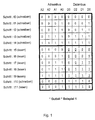
- Figure 1 shows a so-called good case using the example of each 4 bit wide address and data bus, i.e. one episode of test bit patterns according to the invention in the event that the The lines of the address and data bus are error-free.
- the four bits A0, A1, A2, A3 of the address bus with an address bit check pattern like this proves that all bits have the same binary value, in the example in FIG. 1, the value 0000.
- the sequence of writing steps four bits D0, D1, D2, D3 of the data bus with an address bit check pattern so assigned that all bits are also the same Binary value, also in the example of Figure 1 0000.
- too other values are specified in the first step t0.
- each subsequent step in the sequence the writing steps t1, t2, t3, starting with the down or most significant bit in the address and in the data bit pattern, the respective neighboring bits compared to the previous one Step assigned complementary binary significance, until all in the last step t4 of the sequence of writing steps Bits A0, A1, A2, A3 and D0, D1, D2, D3 of the address and data bus a complementary value to the first step t0 exhibit.
- this has the consequence that in the writing steps t1, t2, t3 the address bit check pattern 0001, 0011, 0111 on the address bus and the data bit check pattern 0001, 0011, 0111 on the data bus.
- the last Write step t4 then occurs as an address and data bit check pattern the combination 1111.
- a sequence of reading steps t5 to t9 now closes on.
- the data bit check patterns, which into the cells addressed using the address bit check pattern of the electronic circuit were rewritten be read out.
- the data bit patterns read D0, D1, D2, D3 of the data bus, which in the sequence of reading steps t5 to t9 show the reading result are in figure 1 underlined.
- the read data bit patterns are now the result of test steps with those in the previous series of writing steps data bit check patterns written in the electronic circuit compared. Occur in such a comparison Deviations between the data bit patterns and the data bit check patterns on, in particular with the help of a so-called pattern comparison, the faulty line be localized on the address or data bus.
- Pattern comparison is based on address or data bit error patterns. These represent a library of possible ones Defect patterns, when they occur to a defect certain line of the address or data bus closed can be. Can now at least one written by one Data bit error pattern deviating, read data bit pattern assigned to an available address or data bit error pattern localization of the associated faulty Address or data bus line possible.
- the data bit check pattern in write step t10 is according to the invention selected so that at least the bit of the data bit check pattern has the same binary value as that bit of the data bit check pattern, its binary significance in the second writing step compared to the first Writing step was complemented.
- bit D0 of the data bit check pattern has the same binary significance 0 has like the bit D0 of the data bit check pattern in the first Write step t1, since its binary significance in comparison complemented in the second writing step t2 has been.
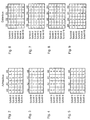
- FIGs 2 to 5 are the example of 4 bits each wide address buses with bits A0, A1, A2, A3 and a first Sequence of writing steps t0 to t4 further, according to the invention possible sequences of address bit check patterns are shown.
- Figure 3 are the valences of the address bit check pattern in the first step 1111, in the following steps 1110, 1100, 1000 and in the last step 0000.
- Figure 4 are the valences of the address bit check pattern in the first step 0000, in the following steps 1000, 1100, 1110 and in the last step 1111.
- Figure 5 are the values of the address bit check pattern in the first step 1111, in the following steps 0111, 0011, 0001 and in last step 0000.
- FIGS. 6 to 9 are also based on the example of each 4 bit wide data buses with bits D0, D1, D2, D3 and one first sequence of writing steps t0 to t4 inclusive the additional writing step t10 further, according to the invention possible sequences of data bit check patterns are shown.
- the values of the data bit check pattern are shown in FIG first step 0000, in the following steps 0001, 0011, 0111 and in the last step 1111.
- step t10 at least the data bit D0 have the significance 0, while the values of the other bits D1, D2, D3 can be chosen freely can what is symbolized by the identifier "d".
- FIG 7 are the weights of the data bit check pattern in the first Step 1111, in the following steps 1110, 1100, 1000 and in the last step 0000.
- the data bit D0 have the value 1, while the Values of the remaining bits D1, D2, D3 can be freely selected can what is symbolized by the identifier "d".
- Figure 8 are the weights of the data bit check pattern in the first Step 0000, in the following steps 1000, 1100, 1110 and in the last step 1111. At least in step t10 the data bit D3 have the value 0, while the Values of the other bits D0, D1, D2 can be freely selected can what is symbolized by the identifier "d”.
- Figure 9 are the weights of the data bit check pattern in the first Step 1111, in the following steps 0111, 0011, 0001 and in the last step 0000. At least in step t10 the data bit D3 have the value 1, while the Values of the other bits D0, D1, D2 can be freely selected can what is symbolized by the identifier "d".
- step t1 Data bit check pattern 0001 written in this cell, and thereby the data bit check pattern written in the previous step t0 0000 overwritten.
- This process in particular detected in reading step t5, because instead of Data bit pattern 0000 the data bit pattern 0001 is read.
- the sequence of those recorded in reading steps t5 to t9 and t11 Data bit patterns and their deviation from the "good case" of the figure 1, i.e. the error pattern that occurs is characteristic for an error on the address bus line A0.
- This can be performed in a series of test steps, e.g. through a pattern comparison the acquired data bit pattern with a library of data bit error patterns can be detected.
- FIG. 11 also shows a sequence of test bit patterns in accordance with of the invention in the event that the data line D0 of the data bus has an "open 0" error.
- the individual Write and read steps for the values on the line D0 of the data bus occurring, error-related deviations compared to the "good case” of Figure 1 are by circles characterized. So D0 remains on the basis of the assumed "open 0" error of this line in steps t1 to t4 and t6 to t9 on the binary weight 0 instead of the weight 1 to be accepted.
- the steps t1 to t4 incorrectly data bit check pattern 0000, 0010, 0110, 1110 instead of the data bit check pattern 0001, 0011, 0111, 1111 written in the respective addressed cells become.
- This process is particularly important in the reading steps t5 to t9 and t11 are detected.
- the consequence of the reading steps t5 to t9 and t11 detected data bit patterns and their Deviation from the "good case" of Figure 1, i.e. the occurring Error pattern, is characteristic of an error the data bus line D0.
- This can be done in a series of test steps, e.g. by a pattern comparison of the detected data bit patterns with a library of data bit error patterns, can be detected.
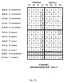
- FIG. 12 shows a sequence of check bit patterns according to the invention in the event that the address line A0 of Address bus has an "open 1" error.
- the individual Write and read steps for the values on the lines A0, D0 of the address and data bus occurring, error-related Deviations from the "good case” of Figure 1 are marked with circles. So A0 remains on the ground the assumed "open 1" error of this line in the Steps t0 and t5 on binary valence 1 instead of Value 0 to be assumed. As a result, the Steps t0, t1 and t5, t6 and t10, t11 in an incorrect manner the same memory cell is addressed.
- step t1 data bit check pattern 0001 is thus written into this cell, and thereby the one in the previous step t0 overwritten data bit check pattern 0000 overwritten.
- This Process is detected in particular in reading step t5, since the data bit pattern instead of the data bit pattern 0000 0001 is read.
- the consequence of the in the reading steps t5 to t9 and t11 detected data bit patterns and their deviation from "Good case" of Figure 1, i.e. the error pattern that occurs, is characteristic of an error on the address bus line A0. This can be done in a series of test steps, e.g. by a pattern comparison of the detected data bit pattern with a Library of data bit error patterns can be detected.
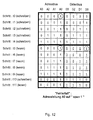
- FIG. 13 shows a sequence of test bit patterns in accordance with of the invention in the event that the data line D0 of the data bus has an "open 1" error.
- the individual Write and read steps for the values on the line D0 of the data bus occurring, error-related deviations compared to the "good case” of Figure 1 are by circles characterized. So D0 remains on the basis of the assumed "open 1" error of this line in steps t5, t10 and t11 on binary valence 1 instead of assuming valence 0.
- steps t0 and t10 the data bit check patterns 0001 and 1111 instead of the data bit check pattern 0000 and 1110 in each addressed cells are written. This process is detected in particular in reading steps t5 and t11.
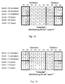
- Figure 14 shows a compilation of the in the Examples of Figures 10, 11, 12, 13 in the form of the steps F5 to t9 and t11 read data bit patterns detected error images I, II, III, IV. It can be seen that the data bit patterns of the four cases are different. In one episode of test steps can therefore be made irrespective of which type of error is present, i.e. regardless of whether an "open 0", “open 1 ",” stuck-at 0 “or” stuck-at 1 "error that is from the line affected by the fault can be clearly identified. This line is now accessible for repair.
- FIGS 21 show Figures 15, 16, 17 examples of so-called "good cases" of Address and data buses with different bus widths, i.e. of address and data buses with faultless cables.
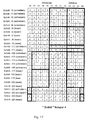
- FIG. 15 shows an example of a 6 bit wide address bus and a 4 bit wide data bus
- FIG. 16 using the example of a 6 bit wide data bus and a 4 bit wide address bus
- FIG. 17 using the example of a 9 bit wide address bus and a 4 bit wide data bus each a sequence of address and data bit check patterns according to the invention.
- the address bus has bits A0, A1 to A5 and the data bus to bits D0, D1 to D3.
- the Address bus thus has a larger bus width than that Data bus.
- in a first sequence of writing steps t0 to t4 initially all bits D0 to D3 of the data bus and those bits of the Address bus, which corresponds to the bits of the data bus Have valences, i.e. bits A0 to A3, with Address and data bit check patterns occupied. Then it closes a sequence of reading steps t5 to t9, with the same selection of bits of the address and data bus accessed becomes like in the previous writing steps.
- Advantageous an additional one then advantageously closes Write step t10 and an additional read step t11.
- step t11 inclusive the example of Figure 1 and is therefore not repeated explained. If no error pattern can be recognized by then, then bits A0 to A3 and D0 to D3 are checked and can be used as be viewed without errors.
- bits of the address or data bus are included address and data bit check patterns selected according to the invention documented, which have the exceeding value. Furthermore, those neighboring bits of the data or Address bus with address and selected according to the invention Data bit check patterns occupied, which in the first sequence of Write, read and test steps already with address or data bit test patterns were occupied and their number, starting at the least significant or most significant bit of this group, corresponds to the number of bits with the highest significance. In the example in FIG. 15, this has the consequence that in the writing steps t12, t13, t14 the bits A4, A5 of the address bus with address bit check patterns and bits D0, D1 of the data bus with data bit check patterns.
- the data bus is 6 bits and Address bus 4 bits wide. Since the test procedure is largely is comparable to the case shown in FIG. 15, are only partially in Figure 16 for simplicity the first three writing steps t0, t1, t2 are shown.
- Figure 17 shows the example of a 9 bit wide Address bus with bits A0 to A8 and a 4 bit wide Data bus with bits D0 to D3 another sequence of Address and data bit check patterns according to the invention.
- Bits A0 to A3 of write, read and test steps Address bus and bits D0 to D3 of the data bus checked.
- Bits A4 to A8 of the address bus with higher value are not yet considered in this phase, and are in figure 17 again assigned "d".
- bits A0 to A3 and D0 to D3 of address and data bus free of errors closes first a second sequence of writing steps t12 to t16, a second sequence of reading steps t17 to t21 and second Sequence of test steps not shown. there are used to check the address bits A4 to A7 these bits and the Bits D0 to D3 of the data bus in one of the previous explanations corresponding way with selected according to the invention Address and data bit check patterns occupied. Bit A8 of the Address bus with higher value is still in this phase not considered. Furthermore, the bits A0 that have already been checked to A3 of the address bus are no longer considered in this phase. All these bits are thus also assigned "d" in FIG. 17.
- bits A4 to A7 of the address bus are error-free, then so conclude a final sequence of two writing steps t22, t23, a last sequence of two reading steps t24, t25 and a final sequence of test steps, not shown on. These are used to test the highest value Address bits A8. In this case, bits D1 to D3 and A0 assigned to "A" by A7, since these have been used in the previous Steps have already been checked.
- FIGS. 18 to 21 each use the example a 6 bit wide address bus and a 4 bit wide one Shown the tests of those address lines, which is the significance of the most significant bit D3 of the Data bus exceeding significance.
- these are the address bits A4, A5, which means a second sequence of writing steps t12, t13, t14 and a second sequence of reading steps t15, t16, t17 checked become. It is assumed that the address bits A0 to A3 and the data bits D0 to D3 each in a first sequence of reading, writing and checking steps checked and error-free are. These first sequences correspond to steps t0 to t11 of e.g. Examples shown in Figures 1 and 15, and therefore do not have to be explained again.
- Figure 18 shows a section of a sequence of check bit patterns according to the invention in the event that the address line A4 of the address bus has an "open 0" error. So A4 remains because of the assumed fault of this line at steps t13, t14 and t16, t17 on the binary valence 0 instead of assuming the value 1. This has to Consequence that in steps t12, t13 and t15, t16 in error Way the same memory cell is addressed. in the Step t13 thus becomes the data bit check pattern dd01 into it Cell, and thereby the previous one Step t12 overwritten data bit check patterns dd00.
- This process is particularly important in the reading step t15 is detected, because instead of the data bit pattern dd00 the data bit pattern dd01 is read.
- the consequence of in the Reading steps t15 to t17 detected data bit patterns and their Deviation from the "good case" e.g. of Figure 1, i.e. that included occurring error pattern is characteristic of an error on the address bus line A4.
- This can be in a sequence of Test steps, e.g. by comparing the samples Data bit patterns with a library of data bit error patterns, can be detected.
- FIG. 19 also shows a section of a sequence of Check bit patterns according to the invention in the event that the Address line A4 of the address bus has an "open 1" error. So A4 persists due to the assumed mistake Line at steps t12 and t15 on the binary Value 1 instead of assuming value 0. This too has the consequence that in steps t12, t13 and t15, t16 in incorrectly addressed the same memory cell becomes.
- step t13 the data bit check pattern is thus again dd01 written in this cell, and thereby the im data bit check patterns written in previous step t12 dd00 overwritten.
- This process is particularly in the Read step t15 is detected because it replaces the data bit pattern dd00 the data bit pattern dd01 is read.
- the consequence the data bit patterns detected in reading steps t15 to t17 and their deviation from the "good case” e.g. of Figure 1, i.e. the the error pattern that occurs is also characteristic for an error on the A4 address bus line.
- FIG. 20 also shows a section of a sequence of Check bit patterns according to the invention in the event that the Address line A5 of the address bus has an "open 0" error. So A5 persists due to the assumed mistake Line at steps t14 and t17 on the binary Value 0 instead of assuming value 1. This has to Consequence that in steps t13, t14 and t16, t17 in error Way the same memory cell is addressed. in the Step t14 thus becomes the data bit check pattern dd11 into it Cell, and thereby the previous one Step t13 overwritten data bit check pattern dd01. This process is particularly important in the reading step t16 is detected because, instead of the data bit pattern dd01 the data bit pattern dd11 is read. The consequence of in the Reading steps t15 to t17 detected data bit patterns and their Deviation from the "good case” e.g. of Figure 1, i.e. that included occurring error pattern is characteristic of an error on the address bus line A5.
- FIG. 21 shows a section of a Sequence of check bit patterns according to the invention for the case that the address line A5 of the address bus has an "open 1" error having. So A5 remains because of the assumed error this line at steps t12, t13 and t15, t16 binary value 1 instead of assuming value 0. As a result, in steps t13, t14 and t16, t17 addressed the same memory cell incorrectly becomes. The data bit check pattern is thus in step t14 dd11 written in this cell, and thereby the one in the previous one Data bit check patterns written in step t13 dd01 overwritten.
- This process is particularly important in the reading step t16 is detected because it replaces the data bit pattern dd01 the data bit pattern dd11 is read.
- the consequence of in the data bit patterns and their read steps t15 to t17 Deviation from the "good case" e.g. of Figure 1, i.e. that included occurring error pattern is characteristic of an error on the address bus line A5.
Landscapes
- Techniques For Improving Reliability Of Storages (AREA)
- Tests Of Electronic Circuits (AREA)
- For Increasing The Reliability Of Semiconductor Memories (AREA)
Abstract
Description
- FIG 1 :
- am Beispiel eines jeweils 4 Bit breiten Adreß- und Datenbusses eine Folge von Prüfbitmustern gemäß der Erfindung für den Fall, daß die Leitungen von Adreß- und Datenbus fehlerfrei sind,
- FIG 2 bis 5 :
- am Beispiel von jeweils 4 Bit breiten Adreßbussen weitere, gemäß der Erfindung mögliche Folgen von Adreßbitprüfmustern,
- FIG 6 bis 9 :
- am Beispiel von jeweils 4 Bit breiten Datenbussen weitere, gemäß der Erfindung mögliche Folgen von Datenbitprüfmustern,
- FIG 10 :
- am Beispiel eines jeweils 4 Bit breiten Adreß- und Datenbusses eine Folge von Prüfbitmustern gemäß der Erfindung für den Fall, daß die Adreßleitung A0 des Adreßbusses einen "open 0" Fehler aufweist,
- FIG 11 :
- am Beispiel eines jeweils 4 Bit breiten Adreß- und Datenbusses eine Folge von Prüfbitmustern gemäß der Erfindung für den Fall, daß die Datenleitung D0 des Datenbusses einen "open 0" Fehler aufweist,
- FIG 12 :
- am Beispiel eines jeweils 4 Bit breiten Adreß- und Datenbusses eine Folge von Prüfbitmustern gemäß der Erfindung für den Fall, daß die Adreßleitung A0 des Adreßbusses einen "open 1" Fehler aufweist,
- FIG 13 :
- am Beispiel eines jeweils 4 Bit breiten Adreß- und Datenbusses eine Folge von Prüfbitmustern gemäß der Erfindung für den Fall, daß die Datenleitung D0 des Datenbusses einen "open 1" Fehler aufweist,
- FIG 14 :
- eine Gegenüberstellung der in den Beispielen der Figuren 10, 11, 12, 13 auftretenden Fehlerbilder auf den Datenleitungen der jeweiligen Datenbusse,
- FIG 15 :
- am Beispiel eines 6 Bit breiten Adreßbusses und eines 4 Bit breiten Datenbusses eine Folge von Prüfbitmustern gemäß der Erfindung für den Fall, daß die Leitungen von Adreß- und Datenbus fehlerfrei sind,
- FIG 16 :
- am Beispiel eines 6 Bit breiten Datenbusses und eines 4 Bit breiten Adreßbusses den Anfang einer Folge von Prüfbitmustern gemäß der Erfindung für den Fall, daß die Leitungen von Adreß- und Datenbus fehlerfrei sind,
- FIG 17 :
- am Beispiel eines 9 Bit breiten Adreßbusses und eines 4 Bit breiten Datenbusses eine Folge von Prüfbitmustern gemäß der Erfindung für den Fall, daß die Leitungen von Adreß- und Datenbus fehlerfrei sind,
- FIG 18 :
- am Beispiel eines 6 Bit breiten Adreßbusses und eines 4 Bit breiten Datenbusses einen Ausschnitt aus einer Folge von Prüfbitmustern gemäß der Erfindung für den Fall, daß die Adreßleitung A4 des Adreßbusses einen "open 0" Fehler aufweist,
- FIG 19 :
- am Beispiel eines 6 Bit breiten Adreßbusses und eines 4 Bit breiten Datenbusses einen Ausschnitt aus einer Folge von Prüfbitmustern gemäß der Erfindung für den Fall, daß die Adreßleitung A4 des Adreßbusses einen "open 1" Fehler aufweist,
- FIG 20 :
- am Beispiel eines 6 Bit breiten Adreßbusses und eines 4 Bit breiten Datenbusses einen Ausschnitt aus einer Folge von Prüfbitmustern gemäß der Erfindung für den Fall, daß die Adreßleitung A5 des Adreßbusses einen "open 0" Fehler aufweist, und
- FIG 21 :
- am Beispiel eines 6 Bit breiten Adreßbusses und eines 4 Bit breiten Datenbusses einen Ausschnitt aus einer Folge von Prüfbitmustern gemäß der Erfindung für den Fall, daß die Adreßleitung A5 des Adreßbusses einen "open 1" Fehler aufweist.

- ABB =
- Adreßbusbreite
- DBB =
- Datenbusbreite.
Claims (3)
- Verfahren zur Überprüfung der Kontaktanschlüsse eines schreib- und lesbaren integrierten, elektronischen Schaltkreises, insbesondere eines Speicherbausteins, an einem Adreß- und einem Datenbus, wobeiA. in mindestens einer ersten Folge von Schreibschritten (t0...t4) der Adreßbus (A0,A1,.) schrittweise mit ausgewählten Adreßbitprüfmustern (.,0011,.) belegt wird und ausgewählte Datenbitprüfmuster (.,1100,.) auf dem Datenbus (D0,D1,.) in den Schaltkreis geschrieben werden,B. in mindestens einer ersten Folge von Leseschritten (t5...t9) der Adreßbus (A0,A1,.) wiederum schrittweise mit den ausgewählten Adreßbitprüfmustern (.,0011,.) belegt wird und die dazugehörigen Datenbitmuster (.,1100,.) auf dem Datenbus (D0,D1,.) aus dem Schaltkreis gelesen werden,C. in mindestens einer ersten Folge von Prüfschritten die gelesenen Datenbitmuster mit den ausgewählten Datenprüfbitmustern verglichen werden und bei Abweichungen, insbesondere durch Mustervergleich mit Adreß- und Datenbitfehlermustern, die fehlerhafte Leitung auf dem Adreßbus (A0,A1,.) bzw. Datenbus (D0,D1,.) lokalisiert wird,
dadurch gekennzeichnet, daßD. Adreß- und Datenbitprüfmuster so ausgewählt sind, daßi) in einem ersten Schritt der ersten Folge von Schreib- bzw. Leseschritten (t0 bzw. t5) die Bits des Adreßbitprüfmusters eine erste, übereinstimmende binäre Wertigkeit (0000 bzw. 1111) aufweisen, undii) im ersten Schritt der ersten Folge von Schreibschritten (t0) die Bits des Datenbitprüfmusters eine zweite, übereinstimmende binäre Wertigkeit (0000 bzw. 1111) aufweisen, undiii) pro folgendem Schritt der jeweiligen Folge von Schreib- bzw. Leseschritten (t1,t2,t3 bzw. t6,t7,t8) beginnend beim nieder- oder höchstwertigsten Bit im Adreß- bzw. Datenbitprüfmuster, dem jeweils benachbarten Bit die im Vergleich zum vorangegangenen Schritt (.,0011,. bzw. .,1100,.) jeweils komplementäre binäre Wertigkeit zugeordnet wird (.,0111,. bzw. .,1000,.), bisiv) in einem letzten Schritt der Folge von Schreibbzw. Leseschritten (t4;t9) alle Bits des Adreßbzw. Datenbitprüfmusters eine zum jeweiligen ersten Schritt komplementäre binäre Wertigkeit (1111 bzw. 0000) aufweisen. - Verfahren nach Anspruch 1, wobei zur Überprüfung von Bits des Adreßbusses (A5,A4) bzw. des Datenbusses (D5,D4), welche eine die Wertigkeit des jeweils höchstwertigsten Bits des Datenbusses (D3) bzw. des Adreßbusses (A3) übersteigende Wertigkeit aufweisen,A. zumindest eine zweite Folge (t12...t17) von Schreib-, Lese- und Prüfschritten durchlaufen wird, und dabeiB. mit ausgewählten Adreß- und Datenbitprüfmustern belegt werdeni) diejenigen Bits des Adreß- bzw. Datenbusses (A5,A4; D5,D4), welche die übersteigende Wertigkeit aufweisen, undii) diejenigen benachbarten Bits des Daten- bzw. Adreßbusses (D1,D0;), welchea) in der ersten Folge von Schreib-, Lese- und Prüfschritten (t0...t9) bereits mit Adreßbzw. Datenbitprüfmustern belegt wurden, undb) deren Anzahl, beginnend beim jeweils niederoder höchstwertigsten Bit dieser Gruppe, der Anzahl der Bits mit der übersteigenden Wertigkeit entspricht.
- Verfahren nach Anspruch 1 oder 2, wobeiA) im Anschluß an die erste Folge von Schreib-, Lese- und Prüfschritten (t0...t9) für dieselben Adreß- und Datenbusbits (A0,A1, ...;D0, D1, ...) jeweils ein zusätzlicher Schreib-, Lese- und Prüfschritt (t10,t11) durchführt wird, und dabei zumindestB) das Datenbitprüfmuster so ausgewählt wird, daß in dem zusätzlichen Schreibschritt (t10) zumindest das Bit (D0) des Datenbitprüfmusters die gleiche binäre Wertigkeit aufweist wie dasjenige Bit des Datenbitprüfmusters, dessen binäre Wertigkeit beim zweiten Schreibschritt (t2) im Vergleich zum ersten Schreibschritt (t1) komplementiert wurde.
Priority Applications (1)
| Application Number | Priority Date | Filing Date | Title |
|---|---|---|---|
| EP98956859A EP1027707B1 (de) | 1997-11-03 | 1998-10-21 | Verfahren zur prüfung der busanschlüsse von beschreib- und lesbaren integrierten, elektronischen schaltkreisen, insbesondere von speicherbausteinen |
Applications Claiming Priority (4)
| Application Number | Priority Date | Filing Date | Title |
|---|---|---|---|
| EP97119180 | 1997-11-03 | ||
| EP97119180A EP0913837A1 (de) | 1997-11-03 | 1997-11-03 | Verfahren zur Prüfung der Busanschlüsse von beschreib- und lesbaren integrierten, elektronischen Schaltkreisen, insbesondere von Speicherbausteinen |
| EP98956859A EP1027707B1 (de) | 1997-11-03 | 1998-10-21 | Verfahren zur prüfung der busanschlüsse von beschreib- und lesbaren integrierten, elektronischen schaltkreisen, insbesondere von speicherbausteinen |
| PCT/EP1998/006673 WO1999023665A1 (de) | 1997-11-03 | 1998-10-21 | Verfahren zur prüfung der busanschlüsse von beschreib- und lesbaren integrierten, elektronischen schaltkreisen, insbesondere von speicherbausteinen |
Publications (2)
| Publication Number | Publication Date |
|---|---|
| EP1027707A1 EP1027707A1 (de) | 2000-08-16 |
| EP1027707B1 true EP1027707B1 (de) | 2002-03-13 |
Family
ID=8227564
Family Applications (2)
| Application Number | Title | Priority Date | Filing Date |
|---|---|---|---|
| EP97119180A Withdrawn EP0913837A1 (de) | 1997-11-03 | 1997-11-03 | Verfahren zur Prüfung der Busanschlüsse von beschreib- und lesbaren integrierten, elektronischen Schaltkreisen, insbesondere von Speicherbausteinen |
| EP98956859A Expired - Lifetime EP1027707B1 (de) | 1997-11-03 | 1998-10-21 | Verfahren zur prüfung der busanschlüsse von beschreib- und lesbaren integrierten, elektronischen schaltkreisen, insbesondere von speicherbausteinen |
Family Applications Before (1)
| Application Number | Title | Priority Date | Filing Date |
|---|---|---|---|
| EP97119180A Withdrawn EP0913837A1 (de) | 1997-11-03 | 1997-11-03 | Verfahren zur Prüfung der Busanschlüsse von beschreib- und lesbaren integrierten, elektronischen Schaltkreisen, insbesondere von Speicherbausteinen |
Country Status (8)
| Country | Link |
|---|---|
| US (1) | US6345372B1 (de) |
| EP (2) | EP0913837A1 (de) |
| JP (1) | JP3583989B2 (de) |
| KR (1) | KR100336530B1 (de) |
| CN (1) | CN1133172C (de) |
| DE (1) | DE59803371D1 (de) |
| TW (1) | TW402721B (de) |
| WO (1) | WO1999023665A1 (de) |
Families Citing this family (29)
| Publication number | Priority date | Publication date | Assignee | Title |
|---|---|---|---|---|
| US6766488B2 (en) * | 2001-10-15 | 2004-07-20 | Nohau Corporation | Compressing information using CAM for narrow bit pattern output |
| TWI245293B (en) * | 2001-11-26 | 2005-12-11 | Winbond Electronics Corp | Method of testing memory with continuous, varying data |
| DE10259300B4 (de) * | 2002-12-18 | 2004-10-07 | Infineon Technologies Ag | Halbleiter-Bauelement-Test-Gerät, Halbleiter-Bauelement-Test-System und Halbleiter-Bauelement-Test-Verfahren zum Testen der Kontaktierung bei übereinanderliegenden Halbleiter-Bauelementen |
| US7036054B2 (en) * | 2003-07-02 | 2006-04-25 | Nokia Corporation | Memory bus checking procedure |
| CN1809820A (zh) * | 2004-06-22 | 2006-07-26 | 三菱电机株式会社 | 电梯电子安全装置用系统 |
| DE102004041553B4 (de) * | 2004-08-27 | 2006-06-29 | Infineon Technologies Ag | Testverfahren zum Bestimmen der Verdrahtung von Schaltungsträgern mit darauf angeordneten Bauelementen |
| US7539912B2 (en) | 2005-12-15 | 2009-05-26 | King Tiger Technology, Inc. | Method and apparatus for testing a fully buffered memory module |
| US7725782B2 (en) * | 2007-01-04 | 2010-05-25 | Gm Global Technology Operations, Inc. | Linked random access memory (RAM) interleaved pattern persistence strategy |
| US7620861B2 (en) * | 2007-05-31 | 2009-11-17 | Kingtiger Technology (Canada) Inc. | Method and apparatus for testing integrated circuits by employing test vector patterns that satisfy passband requirements imposed by communication channels |
| US7757144B2 (en) * | 2007-11-01 | 2010-07-13 | Kingtiger Technology (Canada) Inc. | System and method for testing integrated circuit modules comprising a plurality of integrated circuit devices |
| JP5304030B2 (ja) | 2008-05-30 | 2013-10-02 | 富士通株式会社 | メモリテスト方法およびメモリテスト装置 |
| US7848899B2 (en) * | 2008-06-09 | 2010-12-07 | Kingtiger Technology (Canada) Inc. | Systems and methods for testing integrated circuit devices |
| US8356215B2 (en) * | 2010-01-19 | 2013-01-15 | Kingtiger Technology (Canada) Inc. | Testing apparatus and method for analyzing a memory module operating within an application system |
| US8918686B2 (en) | 2010-08-18 | 2014-12-23 | Kingtiger Technology (Canada) Inc. | Determining data valid windows in a system and method for testing an integrated circuit device |
| JP5581966B2 (ja) * | 2010-10-22 | 2014-09-03 | 株式会社デンソー | 電子装置、及び、これを用いた電動パワーステアリング装置 |
| CN102486938B (zh) * | 2010-12-06 | 2015-01-07 | 北大方正集团有限公司 | 一种快速检测存储器的方法及装置 |
| CN102798816B (zh) * | 2011-05-26 | 2014-11-05 | 上海复旦微电子集团股份有限公司 | 一种用于检测存储器译码电路的测试图形的生成方法 |
| US9003256B2 (en) | 2011-09-06 | 2015-04-07 | Kingtiger Technology (Canada) Inc. | System and method for testing integrated circuits by determining the solid timing window |
| US8724408B2 (en) | 2011-11-29 | 2014-05-13 | Kingtiger Technology (Canada) Inc. | Systems and methods for testing and assembling memory modules |
| US9117552B2 (en) | 2012-08-28 | 2015-08-25 | Kingtiger Technology(Canada), Inc. | Systems and methods for testing memory |
| CN104425040A (zh) * | 2013-08-23 | 2015-03-18 | 辉达公司 | 用于测试存储器的方法和系统 |
| CN107656188B (zh) * | 2017-09-11 | 2023-12-29 | 深圳市爱协生科技股份有限公司 | 一种芯片的测试系统及其方法 |
| CN109872754B (zh) * | 2019-02-15 | 2021-02-26 | 长江存储科技有限责任公司 | 数据编程方法及装置、存储器及存储介质 |
| CN111627490A (zh) * | 2020-05-22 | 2020-09-04 | 浙江大华技术股份有限公司 | 同步动态随机存储器测试方法和装置 |
| CN111923606B (zh) * | 2020-06-30 | 2022-03-29 | 厦门汉印电子技术有限公司 | 一种打印机 |
| CN112595950A (zh) * | 2020-10-10 | 2021-04-02 | 永诺电气有限公司 | 电力仪表电路板检测装置 |
| CN117253529A (zh) * | 2022-06-10 | 2023-12-19 | 中电海康集团有限公司 | 获取磁性随机存储器短路故障地址的方法以及测试系统 |
| TWI847340B (zh) * | 2022-11-01 | 2024-07-01 | 瑞昱半導體股份有限公司 | 記憶體測試電路 |
| CN119207533B (zh) * | 2023-06-19 | 2025-09-26 | 长鑫存储技术有限公司 | 存储器测试方法、装置与测试设备 |
Family Cites Families (2)
| Publication number | Priority date | Publication date | Assignee | Title |
|---|---|---|---|---|
| US5541942A (en) * | 1994-06-14 | 1996-07-30 | Microsoft Corporation | Method and system for testing memory utilizing specific bit patterns |
| US5668816A (en) * | 1996-08-19 | 1997-09-16 | International Business Machines Corporation | Method and apparatus for injecting errors into an array built-in self-test |
-
1997
- 1997-11-03 EP EP97119180A patent/EP0913837A1/de not_active Withdrawn
-
1998
- 1998-06-01 TW TW087108515A patent/TW402721B/zh not_active IP Right Cessation
- 1998-10-21 JP JP2000519438A patent/JP3583989B2/ja not_active Expired - Fee Related
- 1998-10-21 CN CN988102242A patent/CN1133172C/zh not_active Expired - Fee Related
- 1998-10-21 DE DE59803371T patent/DE59803371D1/de not_active Expired - Lifetime
- 1998-10-21 EP EP98956859A patent/EP1027707B1/de not_active Expired - Lifetime
- 1998-10-21 WO PCT/EP1998/006673 patent/WO1999023665A1/de not_active Ceased
- 1998-10-21 KR KR1020007004796A patent/KR100336530B1/ko not_active Expired - Fee Related
-
2000
- 2000-04-12 US US09/547,683 patent/US6345372B1/en not_active Expired - Lifetime
Also Published As
| Publication number | Publication date |
|---|---|
| US6345372B1 (en) | 2002-02-05 |
| EP1027707A1 (de) | 2000-08-16 |
| WO1999023665A1 (de) | 1999-05-14 |
| DE59803371D1 (de) | 2002-04-18 |
| KR100336530B1 (ko) | 2002-05-11 |
| KR20010031733A (ko) | 2001-04-16 |
| TW402721B (en) | 2000-08-21 |
| JP3583989B2 (ja) | 2004-11-04 |
| JP2003521011A (ja) | 2003-07-08 |
| CN1133172C (zh) | 2003-12-31 |
| EP0913837A1 (de) | 1999-05-06 |
| CN1276085A (zh) | 2000-12-06 |
Similar Documents
| Publication | Publication Date | Title |
|---|---|---|
| EP0913837A1 (de) | Verfahren zur Prüfung der Busanschlüsse von beschreib- und lesbaren integrierten, elektronischen Schaltkreisen, insbesondere von Speicherbausteinen | |
| DE2225841C3 (de) | Verfahren und Anordnung zur systematischen Fehlerprüfung eines monolithischen Halbleiterspeichers | |
| EP1113362B1 (de) | Integrierter Halbleiterspeicher mit einer Speichereinheit zum Speichern von Adressen fehlerhafter Speicherzellen | |
| DE19930169B4 (de) | Testeinrichtung und Verfahren zum Prüfen eines Speichers | |
| DE69504072T2 (de) | Speicherprüfsystem | |
| EP0186040B1 (de) | Integrierter Halbleiterspeicher | |
| EP1055238B1 (de) | Testschaltung und verfahren zum prüfen einer digitalen halbleiter-schaltungsanordnung | |
| EP0990236B1 (de) | Anordnung mit speicherzellen und verfahren zur funktionsüberprüfung von speicherzellen | |
| EP1254461B1 (de) | Testbarer festwertspeicher für datenspeicher-redundanzlogik | |
| EP0214508B1 (de) | Integrierter Halbleiterspeicher | |
| DE10135966A1 (de) | Verfahren zum On-Chip-Testen von Speicherzellen einer integrierten Speicherschaltung | |
| DE102004039831A1 (de) | Multi-Chip-Modul und Verfahren zum Testen | |
| DE102006051591B3 (de) | Verfahren zum Testen eines Speicherchips | |
| DE2441486A1 (de) | Verfahren zur automatischen fehlerermittlung bei elektrischen schaltkreisen und einrichtung zur durchfuehrung des verfahrens | |
| DE10245713B4 (de) | Testsystem und Verfahren zum Testen von Speicherschaltungen | |
| DE102004043063B4 (de) | Verfahren zum Betreiben eines Halbleiter-Bauelements mit einem Test-Modul | |
| DE10133689C2 (de) | Testverfahren und Testvorrichtung für elektronische Speicher | |
| DE10340236B4 (de) | Anordnung mit einer Datenverarbeitungseinrichtung und einem Speicher | |
| EP0729034A2 (de) | Prüfschaltung und Prüfverfahren zur Funktionsprüfung von elektronischen Schaltungen | |
| DE10112560B4 (de) | Verfahren und Vorrichtung zum Prüfen von Schaltungsmodulen | |
| EP0411594A2 (de) | Schaltungsanordnung und Verfahren zur Funktionssicherheitsprüfung für integrierte Halbleiterspeicher | |
| DE10331543B4 (de) | Verfahren zum Testen einer zu testenden Schaltungseinheit und Schaltungsanordnung zur Durchführung des Verfahrens | |
| DE102022125673A1 (de) | Verfahren zum Betreiben einer Prozessorschaltung, um deren Speicherverdrahtung zu testen, sowie Prozessorschaltung und computerlesbares Speichermedium | |
| DE10211571B4 (de) | Vorrichtung und Verfahren zur Überwachung eines Zustandes einer elektronischen Komponente, insbesondere einer Sicherung | |
| DE10143455A1 (de) | Verfahren zum Testen von zu testenden Schaltungseinheiten mit erhöhter Datenkompression für Burn-in |
Legal Events
| Date | Code | Title | Description |
|---|---|---|---|
| PUAI | Public reference made under article 153(3) epc to a published international application that has entered the european phase |
Free format text: ORIGINAL CODE: 0009012 |
|
| 17P | Request for examination filed |
Effective date: 20000417 |
|
| AK | Designated contracting states |
Kind code of ref document: A1 Designated state(s): DE FR GB IE IT |
|
| 17Q | First examination report despatched |
Effective date: 20010130 |
|
| GRAG | Despatch of communication of intention to grant |
Free format text: ORIGINAL CODE: EPIDOS AGRA |
|
| GRAG | Despatch of communication of intention to grant |
Free format text: ORIGINAL CODE: EPIDOS AGRA |
|
| GRAH | Despatch of communication of intention to grant a patent |
Free format text: ORIGINAL CODE: EPIDOS IGRA |
|
| GRAH | Despatch of communication of intention to grant a patent |
Free format text: ORIGINAL CODE: EPIDOS IGRA |
|
| REG | Reference to a national code |
Ref country code: GB Ref legal event code: IF02 |
|
| GRAA | (expected) grant |
Free format text: ORIGINAL CODE: 0009210 |
|
| AK | Designated contracting states |
Kind code of ref document: B1 Designated state(s): DE FR GB IE IT |
|
| PG25 | Lapsed in a contracting state [announced via postgrant information from national office to epo] |
Ref country code: IT Free format text: LAPSE BECAUSE OF FAILURE TO SUBMIT A TRANSLATION OF THE DESCRIPTION OR TO PAY THE FEE WITHIN THE PRESCRIBED TIME-LIMIT;WARNING: LAPSES OF ITALIAN PATENTS WITH EFFECTIVE DATE BEFORE 2007 MAY HAVE OCCURRED AT ANY TIME BEFORE 2007. THE CORRECT EFFECTIVE DATE MAY BE DIFFERENT FROM THE ONE RECORDED. Effective date: 20020313 Ref country code: IE Free format text: LAPSE BECAUSE OF FAILURE TO SUBMIT A TRANSLATION OF THE DESCRIPTION OR TO PAY THE FEE WITHIN THE PRESCRIBED TIME-LIMIT Effective date: 20020313 Ref country code: GB Free format text: LAPSE BECAUSE OF FAILURE TO SUBMIT A TRANSLATION OF THE DESCRIPTION OR TO PAY THE FEE WITHIN THE PRESCRIBED TIME-LIMIT Effective date: 20020313 Ref country code: FR Free format text: LAPSE BECAUSE OF FAILURE TO SUBMIT A TRANSLATION OF THE DESCRIPTION OR TO PAY THE FEE WITHIN THE PRESCRIBED TIME-LIMIT Effective date: 20020313 |
|
| REF | Corresponds to: |
Ref document number: 59803371 Country of ref document: DE Date of ref document: 20020418 |
|
| GBV | Gb: ep patent (uk) treated as always having been void in accordance with gb section 77(7)/1977 [no translation filed] |
Effective date: 20020313 |
|
| REG | Reference to a national code |
Ref country code: IE Ref legal event code: FD4D |
|
| EN | Fr: translation not filed | ||
| PLBE | No opposition filed within time limit |
Free format text: ORIGINAL CODE: 0009261 |
|
| STAA | Information on the status of an ep patent application or granted ep patent |
Free format text: STATUS: NO OPPOSITION FILED WITHIN TIME LIMIT |
|
| 26N | No opposition filed |
Effective date: 20021216 |
|
| PGFP | Annual fee paid to national office [announced via postgrant information from national office to epo] |
Ref country code: DE Payment date: 20141022 Year of fee payment: 17 |
|
| REG | Reference to a national code |
Ref country code: DE Ref legal event code: R081 Ref document number: 59803371 Country of ref document: DE Owner name: POLARIS INNOVATIONS LTD., IE Free format text: FORMER OWNER: QIMONDA AG, 81739 MUENCHEN, DE Ref country code: DE Ref legal event code: R081 Ref document number: 59803371 Country of ref document: DE Owner name: INFINEON TECHNOLOGIES AG, DE Free format text: FORMER OWNER: QIMONDA AG, 81739 MUENCHEN, DE |
|
| REG | Reference to a national code |
Ref country code: DE Ref legal event code: R081 Ref document number: 59803371 Country of ref document: DE Owner name: POLARIS INNOVATIONS LTD., IE Free format text: FORMER OWNER: INFINEON TECHNOLOGIES AG, 85579 NEUBIBERG, DE |
|
| REG | Reference to a national code |
Ref country code: DE Ref legal event code: R119 Ref document number: 59803371 Country of ref document: DE |
|
| PG25 | Lapsed in a contracting state [announced via postgrant information from national office to epo] |
Ref country code: DE Free format text: LAPSE BECAUSE OF NON-PAYMENT OF DUE FEES Effective date: 20160503 |