EP1022768A2 - Condensateur à couche mince résistant à la tension avec structure interdigitale - Google Patents
Condensateur à couche mince résistant à la tension avec structure interdigitale Download PDFInfo
- Publication number
- EP1022768A2 EP1022768A2 EP00200073A EP00200073A EP1022768A2 EP 1022768 A2 EP1022768 A2 EP 1022768A2 EP 00200073 A EP00200073 A EP 00200073A EP 00200073 A EP00200073 A EP 00200073A EP 1022768 A2 EP1022768 A2 EP 1022768A2
- Authority
- EP
- European Patent Office
- Prior art keywords
- dielectric
- thin film
- film capacitor
- tio
- interdigital
- Prior art date
- Legal status (The legal status is an assumption and is not a legal conclusion. Google has not performed a legal analysis and makes no representation as to the accuracy of the status listed.)
- Ceased
Links
Images

Classifications
-
- H—ELECTRICITY
- H01—ELECTRIC ELEMENTS
- H01L—SEMICONDUCTOR DEVICES NOT COVERED BY CLASS H10
- H01L28/00—Passive two-terminal components without a potential-jump or surface barrier for integrated circuits; Details thereof; Multistep manufacturing processes therefor
- H01L28/40—Capacitors
-
- H—ELECTRICITY
- H01—ELECTRIC ELEMENTS
- H01L—SEMICONDUCTOR DEVICES NOT COVERED BY CLASS H10
- H01L28/00—Passive two-terminal components without a potential-jump or surface barrier for integrated circuits; Details thereof; Multistep manufacturing processes therefor
- H01L28/40—Capacitors
- H01L28/55—Capacitors with a dielectric comprising a perovskite structure material
-
- H—ELECTRICITY
- H01—ELECTRIC ELEMENTS
- H01L—SEMICONDUCTOR DEVICES NOT COVERED BY CLASS H10
- H01L28/00—Passive two-terminal components without a potential-jump or surface barrier for integrated circuits; Details thereof; Multistep manufacturing processes therefor
- H01L28/40—Capacitors
- H01L28/60—Electrodes
Definitions
- the invention relates to a thin-film capacitor which has a carrier substrate, has at least two interdigital electrodes and at least one dielectric.
- Dielectric materials with high dielectric constants are used to achieve high capacities in small dimensions in capacitors.
- thin film processes are used to produce dielectrics with ⁇ r > 50 in dielectric thicknesses of 50 nm to 2 ⁇ m.
- a cost-effective method for depositing thin layers with ⁇ r > 50 uses a wet chemical thin film process such as the sol-gel process.
- the base electrode in the thin-film capacitors is a non-noble metal electrode such as an aluminum or copper electrode or a noble metal electrode made of silver, silver alloys or platinum, for example.
- the top electrode As for the base electrode, noble metals such as platinum, silver, silver alloys or NiCr / gold or non-noble metals such as aluminum, nickel or copper are used. These are applied using thin-film processes such as sputtering or chemical deposition from the gas phase. Lithographic processes combined with wet or dry etching steps are used to structure the electrodes. Si wafers, glass or ceramic materials are used as carrier substrate materials. To protect the capacitor structure, a protective layer, for example an organic layer and / or an inorganic layer, is applied by a printing process or a thin-film process. In addition, the capacitors are provided with power supplies either individually or in strips.
- noble metals such as platinum, silver, silver alloys or NiCr / gold or non-noble metals such as aluminum, nickel or copper are used. These are applied using thin-film processes such as sputtering or chemical deposition from the gas phase. Lithographic processes combined with wet or dry etching steps are used to structure the electrodes. Si wafer
- the layers of the dielectric contribute to the capacitance behavior of the capacitor.
- the dielectric contains a ferroelectric ceramic material.
- Ferroelectric ceramic materials have a large relative dielectric constant ⁇ r and enable high capacities in small dimensions.
- a barrier layer is applied to the carrier substrate is.
- a barrier layer can be used to avoid reactions with the dielectric or short circuits in the case of carrier substrates with a rough surface, for example Al 2 O 3 .
- the dielectric can have 3 multiple layers, for example double, triple or Quadruple layers.
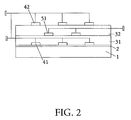
- a multilayer structure with three or more staggered interdigital electrodes be used.
- FIG. 2 shows such a multilayer structure with three offset interdigital electrodes 41, 42 and 51 and two dielectrics 31 and 32 are shown.
- Thin film capacitors are located over a first interdigital one Electrode 41 first has a first dielectric 31, a second interdigital one above it Electrode 51, overlying a second dielectric 32 and a third interdigital Electrode 42.
- the first interdigital electrode 41 and the third interdigital electrode 42 happened in parallel.
- a carrier substrate 1 made of glass is provided with a barrier layer 2 made of TiO 2 .
- a lower interdigital electrode 4 made of Ti / Pt is applied to this barrier layer 2.
- a dielectric 3 made of BaTiO 3 is located above the lower interdigital electrode 4.
- Table 3 shows the average capacitance values C and the operating voltages U rated for thin-film capacitors with interdigital electrodes (parameters according to Table 2) and lanthanum-doped PZT dielectric (layer thicknesses according to Table 1). Average capacitance values C for thin film capacitors with interdigital electrodes and lanthanum doped PZT dielectric. Finger distance [ ⁇ m] Capacitance C [pF] Operating voltage U rated [V] 10th 6.3 200 5 10.8 100 3rd 17.5 60
Applications Claiming Priority (2)
| Application Number | Priority Date | Filing Date | Title |
|---|---|---|---|
| DE19902029 | 1999-01-20 | ||
| DE19902029A DE19902029A1 (de) | 1999-01-20 | 1999-01-20 | Spannungsfester Dünnschichtkondensator mit Interdigitalstruktur |
Publications (2)
| Publication Number | Publication Date |
|---|---|
| EP1022768A2 true EP1022768A2 (fr) | 2000-07-26 |
| EP1022768A3 EP1022768A3 (fr) | 2004-05-06 |
Family
ID=7894783
Family Applications (1)
| Application Number | Title | Priority Date | Filing Date |
|---|---|---|---|
| EP00200073A Ceased EP1022768A3 (fr) | 1999-01-20 | 2000-01-11 | Condensateur à couche mince résistant à la tension avec structure interdigitale |
Country Status (4)
| Country | Link |
|---|---|
| US (1) | US6999297B1 (fr) |
| EP (1) | EP1022768A3 (fr) |
| JP (1) | JP2000216052A (fr) |
| DE (1) | DE19902029A1 (fr) |
Cited By (1)
| Publication number | Priority date | Publication date | Assignee | Title |
|---|---|---|---|---|
| WO2002075780A3 (fr) * | 2001-03-21 | 2004-02-05 | Koninkl Philips Electronics Nv | Dispositif électronique |
Families Citing this family (35)
| Publication number | Priority date | Publication date | Assignee | Title |
|---|---|---|---|---|
| US8744384B2 (en) | 2000-07-20 | 2014-06-03 | Blackberry Limited | Tunable microwave devices with auto-adjusting matching circuit |
| US8064188B2 (en) | 2000-07-20 | 2011-11-22 | Paratek Microwave, Inc. | Optimized thin film capacitors |
| DE102005017655B4 (de) | 2005-04-15 | 2008-12-11 | Polyic Gmbh & Co. Kg | Mehrschichtiger Verbundkörper mit elektronischer Funktion |
| US7869186B2 (en) * | 2005-11-14 | 2011-01-11 | Paratek Microwave, Inc. | High Q and low stress capacitor electrode array |
| US9406444B2 (en) | 2005-11-14 | 2016-08-02 | Blackberry Limited | Thin film capacitors |
| US7711337B2 (en) | 2006-01-14 | 2010-05-04 | Paratek Microwave, Inc. | Adaptive impedance matching module (AIMM) control architectures |
| US7985995B2 (en) | 2006-08-03 | 2011-07-26 | Micron Technology, Inc. | Zr-substituted BaTiO3 films |
| US7714676B2 (en) | 2006-11-08 | 2010-05-11 | Paratek Microwave, Inc. | Adaptive impedance matching apparatus, system and method |
| US7535312B2 (en) | 2006-11-08 | 2009-05-19 | Paratek Microwave, Inc. | Adaptive impedance matching apparatus, system and method with improved dynamic range |
| US7917104B2 (en) | 2007-04-23 | 2011-03-29 | Paratek Microwave, Inc. | Techniques for improved adaptive impedance matching |
| US8213886B2 (en) | 2007-05-07 | 2012-07-03 | Paratek Microwave, Inc. | Hybrid techniques for antenna retuning utilizing transmit and receive power information |
| US7991363B2 (en) | 2007-11-14 | 2011-08-02 | Paratek Microwave, Inc. | Tuning matching circuits for transmitter and receiver bands as a function of transmitter metrics |
| US8072285B2 (en) | 2008-09-24 | 2011-12-06 | Paratek Microwave, Inc. | Methods for tuning an adaptive impedance matching network with a look-up table |
| US8472888B2 (en) | 2009-08-25 | 2013-06-25 | Research In Motion Rf, Inc. | Method and apparatus for calibrating a communication device |
| US9026062B2 (en) | 2009-10-10 | 2015-05-05 | Blackberry Limited | Method and apparatus for managing operations of a communication device |
| US8803631B2 (en) | 2010-03-22 | 2014-08-12 | Blackberry Limited | Method and apparatus for adapting a variable impedance network |
| SG184929A1 (en) | 2010-04-20 | 2012-11-29 | Paratek Microwave Inc | Method and apparatus for managing interference in a communication device |
| US9379454B2 (en) | 2010-11-08 | 2016-06-28 | Blackberry Limited | Method and apparatus for tuning antennas in a communication device |
| US8712340B2 (en) | 2011-02-18 | 2014-04-29 | Blackberry Limited | Method and apparatus for radio antenna frequency tuning |
| US8655286B2 (en) | 2011-02-25 | 2014-02-18 | Blackberry Limited | Method and apparatus for tuning a communication device |
| US8594584B2 (en) | 2011-05-16 | 2013-11-26 | Blackberry Limited | Method and apparatus for tuning a communication device |
| EP2740221B1 (fr) | 2011-08-05 | 2019-06-26 | BlackBerry Limited | Procédé et appareil pour un réglage de bande dans un dispositif de communication |
| US8948889B2 (en) | 2012-06-01 | 2015-02-03 | Blackberry Limited | Methods and apparatus for tuning circuit components of a communication device |
| US20130342953A1 (en) * | 2012-06-20 | 2013-12-26 | University Of Dayton | High voltage non-coplanar interdigitated varactor |
| US9350405B2 (en) | 2012-07-19 | 2016-05-24 | Blackberry Limited | Method and apparatus for antenna tuning and power consumption management in a communication device |
| CN102832195A (zh) * | 2012-08-27 | 2012-12-19 | 集美大学 | 三维电容结构 |
| US10404295B2 (en) | 2012-12-21 | 2019-09-03 | Blackberry Limited | Method and apparatus for adjusting the timing of radio antenna tuning |
| US9374113B2 (en) | 2012-12-21 | 2016-06-21 | Blackberry Limited | Method and apparatus for adjusting the timing of radio antenna tuning |
| KR102032382B1 (ko) * | 2013-01-31 | 2019-10-16 | 삼성디스플레이 주식회사 | 표시장치의 커패시터 제조 방법 및 그에 따라 제조된 커패시터를 구비하는 표시장치 |
| US9438319B2 (en) | 2014-12-16 | 2016-09-06 | Blackberry Limited | Method and apparatus for antenna selection |
| US20160293334A1 (en) * | 2015-03-31 | 2016-10-06 | Tdk Corporation | Thin film capacitor |
| US20170047276A1 (en) * | 2015-08-13 | 2017-02-16 | Advanced Semiconductor Engineering, Inc. | Semiconductor device package and method of manufacturing the same |
| EP3549232A1 (fr) * | 2016-12-02 | 2019-10-09 | Carver Scientific, Inc. | Dispositif mémoire et dispositif de stockage d'énergie capacitif |
| US10686031B2 (en) | 2018-03-27 | 2020-06-16 | Qualcomm Incorporated | Finger metal-oxide-metal (FMOM) capacitor |
| CN114823139B (zh) * | 2022-04-29 | 2024-01-30 | 厦门松元电子股份有限公司 | 一种抗雷击波的高耐压陶瓷介质材料、陶瓷电容器及其制备方法 |
Citations (3)
| Publication number | Priority date | Publication date | Assignee | Title |
|---|---|---|---|---|
| JPH07202123A (ja) * | 1993-12-28 | 1995-08-04 | Nec Corp | 半導体結合コンデンサ |
| JPH07283076A (ja) * | 1994-04-15 | 1995-10-27 | Nippon Telegr & Teleph Corp <Ntt> | キャパシタ |
| EP0823718A2 (fr) * | 1996-07-31 | 1998-02-11 | Philips Patentverwaltung GmbH | Dispositif avec condensateur |
Family Cites Families (4)
| Publication number | Priority date | Publication date | Assignee | Title |
|---|---|---|---|---|
| US3596370A (en) * | 1969-12-11 | 1971-08-03 | Gen Electric | Thin film capacitor |
| US4410867A (en) * | 1978-12-28 | 1983-10-18 | Western Electric Company, Inc. | Alpha tantalum thin film circuit device |
| US4453199A (en) * | 1983-06-17 | 1984-06-05 | Avx Corporation | Low cost thin film capacitor |
| US5122923A (en) * | 1989-08-30 | 1992-06-16 | Nec Corporation | Thin-film capacitors and process for manufacturing the same |
-
1999
- 1999-01-20 DE DE19902029A patent/DE19902029A1/de not_active Withdrawn
-
2000
- 2000-01-11 EP EP00200073A patent/EP1022768A3/fr not_active Ceased
- 2000-01-18 JP JP2000008485A patent/JP2000216052A/ja not_active Withdrawn
- 2000-01-18 US US09/483,923 patent/US6999297B1/en not_active Expired - Fee Related
Patent Citations (3)
| Publication number | Priority date | Publication date | Assignee | Title |
|---|---|---|---|---|
| JPH07202123A (ja) * | 1993-12-28 | 1995-08-04 | Nec Corp | 半導体結合コンデンサ |
| JPH07283076A (ja) * | 1994-04-15 | 1995-10-27 | Nippon Telegr & Teleph Corp <Ntt> | キャパシタ |
| EP0823718A2 (fr) * | 1996-07-31 | 1998-02-11 | Philips Patentverwaltung GmbH | Dispositif avec condensateur |
Cited By (2)
| Publication number | Priority date | Publication date | Assignee | Title |
|---|---|---|---|---|
| WO2002075780A3 (fr) * | 2001-03-21 | 2004-02-05 | Koninkl Philips Electronics Nv | Dispositif électronique |
| US6936877B2 (en) | 2001-03-21 | 2005-08-30 | Koninklijke Philips Electronics N.V. | Integrated circuit including a capacitor with a high capacitance density |
Also Published As
| Publication number | Publication date |
|---|---|
| DE19902029A1 (de) | 2000-07-27 |
| EP1022768A3 (fr) | 2004-05-06 |
| US6999297B1 (en) | 2006-02-14 |
| JP2000216052A (ja) | 2000-08-04 |
Similar Documents
| Publication | Publication Date | Title |
|---|---|---|
| EP1022768A2 (fr) | Condensateur à couche mince résistant à la tension avec structure interdigitale | |
| DE3535059C2 (fr) | ||
| EP0823718B1 (fr) | Dispositif avec condensateur | |
| EP0459575B1 (fr) | Procédé de fabrication de condensateurs à une couche | |
| DE102005026731B4 (de) | Mehrschichtchipvaristor | |
| EP0902954A1 (fr) | Condensateur multicouche a film mince | |
| EP1043741A2 (fr) | Condensateur en couches minces dépendant de la tension | |
| EP2517218B1 (fr) | Varactor et sa methode de fabrication | |
| DE19841402B4 (de) | Verfahren zur Herstellung eines Kondensators eines Halbleiterbauelementes | |
| EP1024535A2 (fr) | Circuit à film mince avec composant | |
| DE60128172T2 (de) | Dielektrische keramische Zusammensetzung, elektronisches Gerät, und Verfahren zu ihrer Herstellung | |
| EP0914677B1 (fr) | Structure stratiforme comportant une couche ferroelectrique et procede de production correspondant | |
| DE19613669A1 (de) | Verfahren zur Herstellung eines Halbleiterelements | |
| DE112012004389T5 (de) | Laminatartiger Halbleiterkeramikkondensator mit Varistorfunktionalität und Verfahren zum Herstellen desselben | |
| EP1024593B1 (fr) | Composant à plusieurs éléments | |
| DE102004047007B4 (de) | Verfahren für das Herstellen eines Keramiksubstrats für elektronische Dünnschicht-Bauelemente | |
| DE19902769A1 (de) | Keramisches, passives Bauelement | |
| DE10161286A1 (de) | Integriertes Halbleiterprodukt mit Metall-Isolator-Metall-Kondensator | |
| DE19651554C2 (de) | Halbleiterbauelement, das gegen elektromagnetische Störungen geschützt ist | |
| DE10009762B4 (de) | Herstellungsverfahren für einen Speicherkondensator mit einem Dielektrikum auf der Basis von Strontium-Wismut-Tantalat | |
| EP0905786B1 (fr) | Condensateur ayant une couche de barrière d'un phosphure, d'un arséniure, our d'un sulfure d'un métal de transition | |
| WO2001018830A1 (fr) | Condensateur en couche mince | |
| DE19640218C2 (de) | Integrierte Halbleiterspeicheranordnung mit Speicherkondensatoren | |
| DE3840410C2 (fr) | ||
| DE19737323A1 (de) | Dünnschichtkondensator mit Schichtelektrode |
Legal Events
| Date | Code | Title | Description |
|---|---|---|---|
| PUAI | Public reference made under article 153(3) epc to a published international application that has entered the european phase |
Free format text: ORIGINAL CODE: 0009012 |
|
| AK | Designated contracting states |
Kind code of ref document: A2 Designated state(s): AT BE CH CY DE DK ES FI FR GB GR IE IT LI LU MC NL PT SE |
|
| AX | Request for extension of the european patent |
Free format text: AL;LT;LV;MK;RO;SI |
|
| RAP1 | Party data changed (applicant data changed or rights of an application transferred) |
Owner name: KONINKLIJKE PHILIPS ELECTRONICS N.V. Owner name: PHILIPS CORPORATE INTELLECTUAL PROPERTY GMBH |
|
| RAP1 | Party data changed (applicant data changed or rights of an application transferred) |
Owner name: KONINKLIJKE PHILIPS ELECTRONICS N.V. Owner name: PHILIPS INTELLECTUAL PROPERTY & STANDARDS GMBH |
|
| PUAL | Search report despatched |
Free format text: ORIGINAL CODE: 0009013 |
|
| AK | Designated contracting states |
Kind code of ref document: A3 Designated state(s): AT BE CH CY DE DK ES FI FR GB GR IE IT LI LU MC NL PT SE |
|
| AX | Request for extension of the european patent |
Extension state: AL LT LV MK RO SI |
|
| RIC1 | Information provided on ipc code assigned before grant |
Ipc: 7H 01L 27/08 B Ipc: 7H 01L 21/02 A |
|
| 17P | Request for examination filed |
Effective date: 20041108 |
|
| AKX | Designation fees paid |
Designated state(s): DE FR GB |
|
| 17Q | First examination report despatched |
Effective date: 20050217 |
|
| RAP1 | Party data changed (applicant data changed or rights of an application transferred) |
Owner name: NXP B.V. |
|
| STAA | Information on the status of an ep patent application or granted ep patent |
Free format text: STATUS: THE APPLICATION HAS BEEN REFUSED |
|
| 18R | Application refused |
Effective date: 20071012 |