EP1020024B1 - Filteranordnung und slope-detector für quadraturamplitudenmodulierte signale - Google Patents
Filteranordnung und slope-detector für quadraturamplitudenmodulierte signale Download PDFInfo
- Publication number
- EP1020024B1 EP1020024B1 EP98952553A EP98952553A EP1020024B1 EP 1020024 B1 EP1020024 B1 EP 1020024B1 EP 98952553 A EP98952553 A EP 98952553A EP 98952553 A EP98952553 A EP 98952553A EP 1020024 B1 EP1020024 B1 EP 1020024B1
- Authority
- EP
- European Patent Office
- Prior art keywords
- channel
- signal
- output
- cross branch
- register
- Prior art date
- Legal status (The legal status is an assumption and is not a legal conclusion. Google has not performed a legal analysis and makes no representation as to the accuracy of the status listed.)
- Expired - Lifetime
Links
Images


Classifications
-
- H—ELECTRICITY
- H04—ELECTRIC COMMUNICATION TECHNIQUE
- H04L—TRANSMISSION OF DIGITAL INFORMATION, e.g. TELEGRAPHIC COMMUNICATION
- H04L27/00—Modulated-carrier systems
- H04L27/10—Frequency-modulated carrier systems, i.e. using frequency-shift keying
- H04L27/14—Demodulator circuits; Receiver circuits
- H04L27/144—Demodulator circuits; Receiver circuits with demodulation using spectral properties of the received signal, e.g. by using frequency selective- or frequency sensitive elements
- H04L27/148—Demodulator circuits; Receiver circuits with demodulation using spectral properties of the received signal, e.g. by using frequency selective- or frequency sensitive elements using filters, including PLL-type filters
-
- H—ELECTRICITY
- H04—ELECTRIC COMMUNICATION TECHNIQUE
- H04L—TRANSMISSION OF DIGITAL INFORMATION, e.g. TELEGRAPHIC COMMUNICATION
- H04L27/00—Modulated-carrier systems
- H04L27/32—Carrier systems characterised by combinations of two or more of the types covered by groups H04L27/02, H04L27/10, H04L27/18 or H04L27/26
- H04L27/34—Amplitude- and phase-modulated carrier systems, e.g. quadrature-amplitude modulated carrier systems
- H04L27/38—Demodulator circuits; Receiver circuits
- H04L27/3845—Demodulator circuits; Receiver circuits using non - coherent demodulation, i.e. not using a phase synchronous carrier
- H04L27/3854—Demodulator circuits; Receiver circuits using non - coherent demodulation, i.e. not using a phase synchronous carrier using a non - coherent carrier, including systems with baseband correction for phase or frequency offset
-
- H—ELECTRICITY
- H03—ELECTRONIC CIRCUITRY
- H03D—DEMODULATION OR TRANSFERENCE OF MODULATION FROM ONE CARRIER TO ANOTHER
- H03D1/00—Demodulation of amplitude-modulated oscillations
- H03D1/22—Homodyne or synchrodyne circuits
- H03D1/2245—Homodyne or synchrodyne circuits using two quadrature channels
-
- H—ELECTRICITY
- H03—ELECTRONIC CIRCUITRY
- H03D—DEMODULATION OR TRANSFERENCE OF MODULATION FROM ONE CARRIER TO ANOTHER
- H03D3/00—Demodulation of angle-, frequency- or phase- modulated oscillations
- H03D3/007—Demodulation of angle-, frequency- or phase- modulated oscillations by converting the oscillations into two quadrature related signals
-
- H—ELECTRICITY
- H04—ELECTRIC COMMUNICATION TECHNIQUE
- H04N—PICTORIAL COMMUNICATION, e.g. TELEVISION
- H04N5/00—Details of television systems
- H04N5/14—Picture signal circuitry for video frequency region
- H04N5/20—Circuitry for controlling amplitude response
- H04N5/205—Circuitry for controlling amplitude response for correcting amplitude versus frequency characteristic
-
- H—ELECTRICITY
- H04—ELECTRIC COMMUNICATION TECHNIQUE
- H04N—PICTORIAL COMMUNICATION, e.g. TELEVISION
- H04N5/00—Details of television systems
- H04N5/44—Receiver circuitry for the reception of television signals according to analogue transmission standards
- H04N5/455—Demodulation-circuits
Definitions
- the present invention relates to a filter arrangement for quadrature amplitude modulated (QAM -) signals, which in particular but not exclusively in a frequency domain equalizer can be used for such signals, and a slope detector to detect an inclined position of the range of services of the QAM signal, which is particularly suitable for use in Suitable for connection with the filter arrangement according to the invention is.
- QAM quadrature amplitude modulated
- Quadrature amplitude modulation is used particularly in color television technology for modulating two independent ones Signals, e.g. B. a luminance and one Color difference signal, on a common carrier wave by modulating its amplitude and phase.
- Signals e.g. B. a luminance and one Color difference signal
- To demodulate the QAM signal back to baseband is the QAM signal with one with the original Carrier in phase (cosine) oscillation or one by 90 ° phase - shifted (sine) oscillation multiplied and low pass filtered, giving two signal components become.
- a filter arrangement which is a first channel for a cosine demodulated component of the QAM signal, a second channel for a sinus demodulated Component of the QAM signal, a filter circuit, which receives the two signal components and for each signal component has a transfer function that comes out with this Signal component in phase and out against this by ⁇ / 2 and / or - ⁇ / 2 phase-shifted terms is composed, and a cross branch for tapping from the out of phase Terms of the transfer function corresponding signal components encompassed by the other channel, the cross branch double available and assigned to one of the two channels is.
- a slope detector which is the two components of the QAM signal receives, with a difference level that the difference between a received data value and the one received last but one Data value of the same component
- one Multiplication level which is the product of one of the first Component derived difference value with one of the second component derived forms, with separate channels for which two components are provided and each channel contains a difference level and a multiplication level.
- the object of the invention is filter arrangements for demodulated Specify QAM signals where this double effort largely is avoided.
- a first solution to this problem is the one described first Filter arrangement to provide a switch arrangement, in a first state the entrance of the cross branch with the first and its output with the second channel and in a second state the entrance of the cross branch with the second and connects its output to the first channel.
- the switch arrangement includes one in each channel Switch, the incoming data alternately in the channel or forwarded to the cross branch.
- This allows data values a component that is only used to produce out of phase Terms in the other channel are needed in the channel on which they arrive are suppressed. So the relevant channel is relieved of processing activity, the results of which are not required later.
- the cross branch preferably comprises a multiplier for multiplying by a weighting factor a.
- S Q (z) -ia + z -T / 2 + iaz -T for channels I and Q, where T denotes the clock period of the data of the demodulated signal components.
- a multiplier is sufficient here.
- the value of the factor a is expediently adjustable depending on the distortion of the signal spectrum measured by a slope detector.
- the cross branch preferably comprises a register for delaying a data value by the time T.
- An adder can be assigned to each channel, the Switch arrangement the output signal of the cross branch each alternately one of the two adders for adding to the on the channel in question.
- a further simplification results if, instead of two adders each assigned to a channel only one adder is provided with a first input through a Switches alternate with the first and second channel connected, and a second input to the output of the cross branch is connected.
- a second solution to the problem is with the one described above Slope controller to set up the differential stage so that they alternate data values of the first and second components can receive, and the multiplication level by one equip first register, which is set up to alternate derived from the first and second components Save difference values.
- This first register preferably gives a received one Difference value with a delay of one clock period, according to the time interval between two consecutive Data values.
- a second register that is set up to output the difference value with a delay of three clock periods, and a switch can be provided which alternates the Output of the first and that of the second register with one Multiplier connects.
- Such slope controllers can in particular be a component an inventive used as a frequency domain equalizer Find filter arrangement use.
- the frequency domain equalizer shown in FIG. 5 is known from the article cited at the beginning. It receives a QAM signal via input 1, represented as complex-valued oscillation e i ⁇ t .
- the signal is divided into an (in the drawing upper) I-channel and a (lower) Q-channel.
- a multiplier 3I in the I-channel multiplies the QAM signal by an oscillation 2e i ⁇ 0 t that is in phase with the carrier.
- the portion with the differential frequency is separated from the product and thus one of the two signals modulated onto the carrier is recovered, referred to in the figure as e i ⁇ B t , where ⁇ B for the difference in the basic frequency range between ⁇ and ⁇ 0 stands.
- the second signal designated as -ie i ⁇ B t , is obtained analogously in the Q-channel by multiplication with a vibration ⁇ / 2 out of phase -2ie i ⁇ 0 t and low-pass filtering.
- the two signal components are of course real in practical implementation, the complex notation used here merely means that the I component as a real part and the Q component as a negative imaginary part or, which would mean the same, the Q component as a real part and the I- Component can be understood as an imaginary part of a complex overall signal.
- the filtered data issued with the period T It is therefore only for everyone second of the input values requires a filtered value. Instead of throwing away the unnecessary values at the output, the data through switches 7I, 7Q are already at the input of the Filter arrangement 10 distributed so that unnecessary values also not be calculated. Switch switches 7I and 7Q with a frequency equal to twice the data output frequency the filter arrangement the data I ([2n + 1] T / 2) or Q ([2n + 1] T / 2) on the I or Q channel 17I, 17Q of the filter arrangement 10 'and the data I (nT) and Q (nT) on the Cross branches 9I and 9Q.
- Each cross branch 9I, 9Q comprises a multiplier 11I, 11Q, which receives the data transmitted by the switch 7I and 7Q and multiplies by a weighting factor a.
- the value of a can be set as a function of the detection result of a slope detector, which will be discussed in more detail in connection with FIG. 6.
- the output of the multiplier 11I, 11Q is connected to a register 13I, 13Q and to a first input of an adder 15I, 15Q.
- Register 13I, 13Q outputs the received data value delayed by a clock period T to a second input of the adder.
- the adder 15I takes into account, when adding, the delayed data value with the opposite sign coming from the register; the adder 15Q takes into account the undelayed data with the opposite sign.
- S * Q (z) -a + az -T ,
- a further adder 25I or 25Q is arranged in channel 17I or 17Q and receives data values from switch 7I, 7Q via a delay element (not shown) at a first input.
- the delay element causes a delay of half a clock period, so that if, for example, the value I (0) is present at the input of the I channel 17I of the filter arrangement, the adder 25I receives the value I (-T / 2).
- the filter arrangement 10 thus realizes the desired transfer function S (z).
- This frequency domain equalizer was designed for radio relay applications proposed with data transfer rates up to 60 Mbaud.
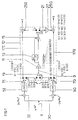
- Fig. 1 shows a first example of a Equalizer with a filter arrangement according to the invention 10 'where this is the case.
- Multipliers 3I, 3Q and low-pass filters 5I, 5Q are the same as in the equalizer of Fig. 5, which is why they are not described again here.
- a switch 7I or 7Q is connected, those arriving at double the symbol frequency Data ... I (-1/2), I (0), I (1/2), I (1), ... or ... Q (-1/2), Q (0), Q (1/2), Q (1), ... alternately on an assigned channel 17I, 17Q, each of which contains an adder 25I or 25Q, or to a first element 19 of a switch arrangement passes.
- This first switch 19 gives the supplied to it Data alternately to a subsequent cross branch 9 further and thus creates a temporally nested data sequence Q (-1), I (-1), Q (0), I (0), Q (1), I (1), ....
- the cross branch 9 comprises a multiplier 11, the from first switch 19 output data with a weighting factor multiplied a.
- the multiplier works with that Twice the symbol frequency f as the clock frequency.
- An adder 15 with two inputs is connected via an input the multiplier 11 and over the other with the output of register 13 connected. It forms the sum of the output data value of register 13 and the negative data value of multiplier 11, i.e. aI (n-1) -aI (n).
- a second switch 21 is provided at the output of the cross branch 9, which synchronizes with the first in such a way Switch is operated that whenever the first Switch 19 receives data from the Q channel, the second switch is connected to the I-channel and vice versa.
- An output of the second switch 21 is connected directly to the adder 25I of the I-channel 17I.
- a delay element (not shown) in the I channel ensures that when a value aQ (n-1) -aQ (n) is output from the cross branch to the adder 15I, the value I (n-1/2) at its other input is applied.
- the adder 25I then outputs the equalized data I (n-1/2) + aQ (n-1) - aQ (n) out.
- the second output of the second switch 21 is connected to the Q-channel adder 25Q via a sign exchanger 27, so that data values are each equalized on the Q-channel 17Q Q (n-1/2) - aI (n-1) + aI (n) be issued.
- the difference between the power densities in the upper and lower sideband of the transmitted QAM signal must be determined.
- 6 shows a slope detector with which this difference is possible on the signal transformed into the baseband.
- the upper and lower sidebands correspond to positive and negative "directions of rotation" of the QAM signal.
- F ub 1 + iz -1 - e.g. -2 - iz -3 respectively.
- F lb -1 + iz -1 + z -2 - iz -3 are separated, the indices ub standing for the upper side band (upper band) and lb for the lower side band (lower band).
- the sum I u 2 - I l 2 + Q u 2 - Q l 2 can be calculated with the slope detector shown in FIG. 6.
- the slope detector receives the two components of a QAM signal on separate inputs 51I, 51Q of separate circuit branches.
- a difference stage each consisting of a register 53I, 53Q which delays by two clocks and an adder 55I, 53Q with an inverting input, forms the difference between a received data value and the data value of the same component received two clocks earlier.
- the output signal of each adder 55I, 55Q is connected to a clock delay register 57I, 57Q and an input of a multiplier 59Q, 59I of the other circuit branch.
- the second input of the multiplier 59I, 59Q is connected to the output of the register 57I, 57Q of the same circuit branch.
- adders 55I, 55Q give the values -I (0) + I (-2) and - Q (0) + Q (-2)
- registers 57I, 57Q give the values -I (-1) + I (-3) or -Q (-1) + Q (-3)
- the multipliers 59I, 59Q the values [-I (-1) + I (-3)] [-Q ( 0) + Q (-2)] and [-Q (-1) + Q (-3)] [- I (0) + I (-2)].
- An adder 61 with an inverting input forms the difference between the two products.
- a multiplier for calibrating the result by multiplying by a factor of 4 and an accumulator 83 for time averaging are connected to the output of the adder 61.
- This circuit can be connected in parallel to the equalizer and process the same input signals as this one but can also be connected downstream of the equalizer. In the latter In this case, simple feedback control can be provided which receives the output signal of the slope detector and regulates the factor a so that its output signal is minimal becomes. Because in this case only relative values of the output signal the calibration multiplier can be required omitted.
- Fig. 2 shows a second embodiment of a frequency domain equalizer with a filter arrangement according to the invention 10 ''.
- Multipliers 3I, 3Q, low-pass filters 5I, 5Q and switches 7I, 7Q are the same as for the equalizers of Figs. 5 and 1.
- the first switch 19 of the filter arrangement as well the elements multiplier 11, register 13 and adder 15 of the cross branch 9 are the same as in the filter arrangement 10 'from FIG. 1. These elements are therefore not described again.
- the switch 21 of Fig. 1 is by a switch 23 replaced, the data from channels 17I, 17Q alternately receives and as a time-nested sequence to an adder 25 forwards.
- the cross branch 9 contains a sign exchanger as an additional element 27 ', the data values from the adder 15 alternately of the form aQ (n) -aQ (n-1) or aI (n) -aI (n-1) and the I values with unchanged sign, the Q values but passes on to the adder 25 with the opposite sign.
- the switches 19 and 23 are synchronized with one another in such a way that when the cross branch 9 outputs a value of the form aQ (n) -aQ (n-1), a suitably delayed value I (n-1/2) from the switch 19 at the second input of adder 25 is present, or that a value aI (n) -aI (n-1) on adder 25 meets a value Q (n-1/2).
- the adder 25 thus generates a sequence of data I (-1/2) + aQ (-1) - aQ (0) Q (-1/2) - aI (-1) + aI (0) I (1/2) + aQ (0) - aQ (1) Q (1/2) - aI (0) + aI (1) I (3/2) + aQ (1) - aQ (2) Q (3/2) - aI (1) + aI (2) ..., which alternately result from filtered elements of sequences I and Q.
- This sequence can be demultiplexed and sent to the inputs of the slope detector 6 are applied to the weighting factor a to determine for the equalization.
- FIG. 1 An advantageous embodiment of a slope detector, the are particularly suitable for use with the equalizers from Figs. 1 and 2 is shown in FIG.
- a multiplexer 71 is connected upstream of the slope detector I and Q signal components or data sequences from the outputs of the equalizer of Fig. 1 receives and alternates to one Sequence consisting of I and Q elements ..., I (-1), Q (-1), I (0), Q (0), I (1), Q (1), ...
- this multiplexer can be omitted because the output sequence this equalizer from alternating I and Q values consists.
- the difference level produces a sequence of the form -I (-1) + I (-3), -Q (-1) + (Q (-3), -I (0) + I (-2), -Q (0) + Q (-2) .
- the multiplier receives the value -I (0) + I (-2) directly from adder 55 and the value -Q (-1) + Q (-3) from register 73. fed. Half a cycle later, the values -Q (0) + Q (-2) and -delayed by one and a half cycles from the multiplier are present from register 75 - I (-1) + I (-3). Two products are thus generated for clock 0, each of which represents a measure of I u 2 - I l 2 and Q l 2 - Q u 2 and are based on data from clocks -3 to 0.
- the multiplier 79 gives the two products to a sign exchanger 81 further, the sign of every second reverses incoming value.
- An accumulator 83 adds the values arriving from the sign exchanger to one moving average.
- the sum of two successive output values of the sign exchanger 81 indicates the difference in the power densities I u 2 - I l 2 + Q u 2 - Q l 2 .
- the circuit according to FIG. 3 thus delivers the same result as that from FIG. 6, but does with only one differential stage and without the adder 61, whose function is also taken over by the accumulator 83.
- FIG. 4 shows a further simplified embodiment of the slope detector from FIG. 3.
- register 75 and switch 77 are omitted, so that multiplier 79 always receives delayed values from register 73. It thus forms a series of products of the form [-Q (-1) + (Q (-3)] [-I (0) + I (-2)], [-Q (0) + Q (-2)] [-I (1) + I (-1)], [-Q (1) + Q (-1)] [-I (2) + I (0)], [-Q (2) + Q (0)] [-I (3) + I (1)], ...
- the first and third of the above terms are each a measure for I u 2 - I l 2 , the second and fourth for Q l 2 - Q u 2 .
- This sequence differs from that of the multiplier 79 of the circuit of FIG. 3 in that successive products are not derived in pairs from data of the same clock. Rather, the first I u 2 - I l 2 term derived from data from measures -3 to 0 is followed by a Q l 2 - Q u 2 term, which is calculated from data from measures -2 to 1.
- changes in the power distribution are slow compared to the operating frequency of the slope detector and the output signal of the slope detector used to control factor a is averaged over a large number of cycles, this change has no effect on the output signal.
Landscapes
- Engineering & Computer Science (AREA)
- Signal Processing (AREA)
- Multimedia (AREA)
- Power Engineering (AREA)
- Computer Networks & Wireless Communication (AREA)
- Physics & Mathematics (AREA)
- Spectroscopy & Molecular Physics (AREA)
- Digital Transmission Methods That Use Modulated Carrier Waves (AREA)
- Compression, Expansion, Code Conversion, And Decoders (AREA)
Description
- Fig. 1
- eine erste Ausgestaltung einer erfindungsgemäßen Filteranordnung;
- Fig. 2
- eine zweite Ausgestaltung einer erfindungsgemäßen Filteranordnung;
- Fig. 3
- eine erste Ausgestaltung eines erfindungsgemäßen Slope-Detectors;
- Fig. 4
- eine zweite Ausgestaltung eines erfindungsgemäßen Slope-Detectors;
- Fig. 5
- einen herkömmlichen Frequenzbereichsentzerrer; und
- Fig. 6
- einen herkömmlichen Slope-Detector.
Claims (14)
- Filteranordnung für ein demoduliertes QAM-Signal, mit einem ersten Kanal (17I) für eine cosinusdemodulierte Komponente des QAM-Signals,
einem zweiten Kanal (17Q) für eine sinusdemodulierte Komponente des QAM-Signals,
einer Filterschaltung (10', 10''), die die zwei Signalkomponenten empfängt und für jede Signalkomponente eine Übertragungsfunktion hat, die aus mit dieser Signalkomponente phasengleichen und aus gegen diese um π/2 und/oder -π/2 phasenverschobenen Termen zusammengesetzt ist, und einen Kreuzzweig (9) zum Abgreifen von den phasenverschobenen Termen der Übertragungsfunktion entsprechenden Signalanteilen vom jeweils anderen Kanal umfaßt,
gekennzeichnet durch
eine Schalteranordnung (19, 21; 19, 23), die in einem ersten Zustand den Eingang des Kreuzzweigs (9) mit dem ersten (17I) und seinen Ausgang mit dem zweiten Kanal (17Q) und in einem zweiten Zustand den Eingang des Kreuzzweigs (9) mit dem zweiten (17Q) und seinen Ausgang mit dem ersten Kanal (17I) verbindet. - Filteranordnung nach Anspruch 1,
dadurch gekennzeichnet, daß jeder Kanal (17I, 17Q) einen Schalter (7I, 7Q) umfaßt, der eintreffende Daten alternierend in dem Kanal (17I, 17Q) bzw. auf den Kreuzzweig (9) weiterleitet. - Filter nach Anspruch 1 oder 2,
dadurch gekennzeichnet, daß der Kreuzzweig (9) einen Multiplizierer (11) zum Multiplizieren mit einem Gewichtungsfaktor a eines phasenverschobenen Terms enthält. - Filter nach einem der vorhergehenden Ansprüche,
dadurch gekennzeichnet, daß der Kreuzzweig (9) wenigstens ein Verzögerungsregister (13) enthält. - Filter nach einem der vorhergehenden Ansprüche,
dadurch gekennzeichnet, daß die phasenverschobenen Terme der zwei Übertragungsfunktionen entgegengesetzt gleich sind. - Filter nach einem der vorstehenden Ansprüche,
dadurch gekennzeichnet, daß jedem Kanal (17I, 17Q) ein Addierer (25I, 25Q) zugeordnet ist, der jeweils die Verbindung des Ausgangs des Kreuzzweigs (9) mit dem zugeordneten Kanal (17I, 17Q) bildet. - Filter nach Anspruch 6,
dadurch gekennzeichnet, daß die zwei Addierer (25I, 25Q) den über den Kreuzzweig (9) übertragenen Signalanteil mit jeweils unterschiedlichen Vorzeichen zur auf dem Kanal (17I, 17Q) übertragenen Signalkomponente addieren. - Filter nach einem der Ansprüche 1 bis 5,
gekennzeichnet durch einen Addierer (25) mit einem ersten Eingang, der durch einen Schalter (23) alternierend mit dem ersten bzw. zweiten Kanal (17I, 17Q) verbunden ist, und einem zweiten Eingang, der an den Ausgang des Kreuzzweigs (9) angeschlossen ist. - Filter nach Anspruch 8,
dadurch gekennzeichnet, daß der Kreuzzweig (9) einen Vorzeichenvertauscher (27') enthält, der das Vorzeichen des Signalanteils entsprechend dem Zustand der Schalteranordnung (19, 23) alternierend vertauscht bzw. nicht vertauscht. - Filter nach Anspruch 3,
gekennzeichnet durch einen Slope-Detector, der eine Differenz der Leistungsdichten im oberen und unteren Seitenband des QAM-Signals detektiert und den Gewichtungsfaktor a steuert, um die Differenz zu minimieren. - Slope-Detector, der die zwei Komponenten eines QAM-Signals empfängt, mit einer Differenzstufe (53, 55), die die Differenz zwischen einem empfangenen Datenwert und dem zu vorletzt empfangenen Datenwert derselben Komponente bildet, und einer Multiplikationsstufe (73, 79; 73, 75, 79), die das Produkt eines von der ersten Komponente abgeleiteten Differenzwerts mit einem von der zweiten Komponente abgeleiteten bildet, dadurch gekennzeichnet, daß die Differenzstufe (53, 55) eingerichtet ist, alternierend Datenwerte der ersten und der zweiten Komponente zu empfangen, und daß die Multiplikationsstufe (73, 79; 73, 75, 79) ein erstes Register (73) umfaßt, das eingerichtet ist, um alternierend von der ersten und von der zweiten Komponente abgeleitete Differenzwerte zu speichern.
- Slope-Detector nach Anspruch 11,
dadurch gekennzeichnet, daß das erste Register (73) eingerichtet ist, den Differenzwert mit einer halben Taktperiode Verzögerung auszugeben. - Slope-Detector nach Anspruch 11 oder 12,
dadurch gekennzeichnet, daß die Multiplikationsstufe (73, 75, 79) ein zweites Register (75), das eingerichtet ist, den Differenzwert mit eineinhalb Taktperioden Verzögerung auszugeben, und einen Schalter (77) umfaßt, der alternierend den Ausgang des ersten (73) und den des zweiten Registers (75) mit einem Multiplizierer (79) verbindet. - Filter nach Anspruch 10,
dadurch gekennzeichnet, daß er ein Frequenzbereichsentzerrer ist und einen Slope-Detector nach einem der Ansprüche 11 bis 13 umfaßt.
Applications Claiming Priority (3)
| Application Number | Priority Date | Filing Date | Title |
|---|---|---|---|
| DE19741181A DE19741181A1 (de) | 1997-09-18 | 1997-09-18 | Filteranordnung und Slope-Detector für quadraturamplitudenmodulierte Signale |
| DE19741181 | 1997-09-18 | ||
| PCT/DE1998/002663 WO1999014852A1 (de) | 1997-09-18 | 1998-09-09 | Filteranordnung und slope-detector für quadraturamplitudenmodulierte signale |
Publications (2)
| Publication Number | Publication Date |
|---|---|
| EP1020024A1 EP1020024A1 (de) | 2000-07-19 |
| EP1020024B1 true EP1020024B1 (de) | 2002-04-10 |
Family
ID=7842823
Family Applications (1)
| Application Number | Title | Priority Date | Filing Date |
|---|---|---|---|
| EP98952553A Expired - Lifetime EP1020024B1 (de) | 1997-09-18 | 1998-09-09 | Filteranordnung und slope-detector für quadraturamplitudenmodulierte signale |
Country Status (5)
| Country | Link |
|---|---|
| US (1) | US6353639B1 (de) |
| EP (1) | EP1020024B1 (de) |
| KR (1) | KR20010024144A (de) |
| DE (2) | DE19741181A1 (de) |
| WO (1) | WO1999014852A1 (de) |
Families Citing this family (3)
| Publication number | Priority date | Publication date | Assignee | Title |
|---|---|---|---|---|
| DE10157864B4 (de) | 2001-11-26 | 2006-08-10 | Infineon Technologies Ag | Quadratur-Amplituden-Modulations- (QAM) Empfänger |
| US6968170B2 (en) | 2002-07-16 | 2005-11-22 | Narad Networks, Inc. | Adaptive correction of a received signal frequency response tilt |
| US7187736B2 (en) * | 2003-02-13 | 2007-03-06 | Motorola Inc. | Reducing interference in a GSM communication system |
Family Cites Families (4)
| Publication number | Priority date | Publication date | Assignee | Title |
|---|---|---|---|---|
| FR2595895B1 (fr) * | 1986-03-13 | 1988-05-13 | France Etat | Double demodulateur numerique |
| US4647864A (en) * | 1986-04-21 | 1987-03-03 | General Electric Company | Variable-delay, sine-cosine non-coherent demodulator |
| US4755761A (en) * | 1986-06-26 | 1988-07-05 | General Electric Company | Zero intermediate-frequency demodulator |
| US5781589A (en) * | 1995-04-21 | 1998-07-14 | Harris Corporation | Digital slope detector and method |
-
1997
- 1997-09-18 DE DE19741181A patent/DE19741181A1/de not_active Withdrawn
-
1998
- 1998-09-09 WO PCT/DE1998/002663 patent/WO1999014852A1/de not_active Ceased
- 1998-09-09 EP EP98952553A patent/EP1020024B1/de not_active Expired - Lifetime
- 1998-09-09 DE DE59803771T patent/DE59803771D1/de not_active Expired - Lifetime
- 1998-09-09 KR KR1020007002908A patent/KR20010024144A/ko not_active Withdrawn
-
2000
- 2000-03-20 US US09/531,193 patent/US6353639B1/en not_active Expired - Fee Related
Also Published As
| Publication number | Publication date |
|---|---|
| WO1999014852A1 (de) | 1999-03-25 |
| EP1020024A1 (de) | 2000-07-19 |
| DE59803771D1 (de) | 2002-05-16 |
| US6353639B1 (en) | 2002-03-05 |
| KR20010024144A (ko) | 2001-03-26 |
| DE19741181A1 (de) | 1999-03-25 |
Similar Documents
| Publication | Publication Date | Title |
|---|---|---|
| DE69227537T2 (de) | Verfahren zur Signalverarbeitung | |
| DE2735945C2 (de) | Schaltungsanordnung für die Trägersynchronisierung von kohärenten Phasendemodulatoren | |
| DE69421834T2 (de) | Digitale Taktrückgewinnungsschaltung | |
| DE10243141B4 (de) | Verfahren zur Übertragung von optischen Polarisationsmultiplexsignalen | |
| DE69231879T2 (de) | PSK-Demodulator mit Rückkopplungsschaltung zur Phasen- und Frequenzkorrektur | |
| DE68918421T2 (de) | Kohärenter Demodulator für phasenumgetastete Signale. | |
| DE3341430C2 (de) | ||
| DE2503595A1 (de) | Datenempfaenger fuer synchrone quadraturamplituden-modulierte datensignale | |
| DE69110103T2 (de) | Digitaler Funkempfänger. | |
| JP2510992B2 (ja) | 周波数変調されたデジタル信号用復調器 | |
| DE69318896T2 (de) | FIR-Filtergerät für die Verarbeitung von Zeitmultiplexsignalen | |
| DE102007057378B4 (de) | Detektionsvorrichtung für Zeitbereich-IQ-Fehlanpassung eines OFDM-Empfängers | |
| DE2627446B1 (de) | Anordnung zur kompensation des traegerphasenfehlers in einem empfaenger fuer diskrete datenwerte | |
| DE69013524T2 (de) | Parallel arbeitender adaptiver Transversalentzerrer für digitales Hochgeschwindigkeitsübertragungssystem. | |
| DE69318901T2 (de) | Vorrichtung zur Bearbeitung frequenzmultiplexierter Signale in zeitmultiplexierter Weise | |
| DE60032075T2 (de) | Digitaler Restseitenbandmodulator | |
| DE69733264T2 (de) | Komponententaktrückgewinnungssystem für qam | |
| DE3232357C2 (de) | ||
| DE3241411C2 (de) | ||
| DE69829096T2 (de) | Rahmenstruktur mit einer Mehrzahl von Modulationsarten | |
| EP0350999A2 (de) | Vorrichtung zur Entzerrung und Demodulation binärer phasenstetig winkelmodulierter Datensignale mit Modulationsindex 0,5 | |
| DE60030797T2 (de) | Frequenzkorrektur in Mehrträgerempfängern | |
| DE2317597C3 (de) | Verfahren und Schaltungsanordnung zum Entzerren eines nach Übertragung mittels Phasenmodulation mit linearen Verzerrungen behafteten Signals vor der Demodulation | |
| DE2712474C3 (de) | Demodulationssystem für eine mehrphasig und mehrstufig fiberlagerungsmodulierte Trägerwelle | |
| EP1020024A1 (de) | Filteranordnung und slope-detector für quadraturamplitudenmodulierte signale |
Legal Events
| Date | Code | Title | Description |
|---|---|---|---|
| PUAI | Public reference made under article 153(3) epc to a published international application that has entered the european phase |
Free format text: ORIGINAL CODE: 0009012 |
|
| 17P | Request for examination filed |
Effective date: 20000317 |
|
| AK | Designated contracting states |
Kind code of ref document: A1 Designated state(s): DE ES FR GB IT |
|
| GRAG | Despatch of communication of intention to grant |
Free format text: ORIGINAL CODE: EPIDOS AGRA |
|
| RAP1 | Party data changed (applicant data changed or rights of an application transferred) |
Owner name: MICRONAS MUNICH GMBH |
|
| 17Q | First examination report despatched |
Effective date: 20010531 |
|
| GRAG | Despatch of communication of intention to grant |
Free format text: ORIGINAL CODE: EPIDOS AGRA |
|
| GRAH | Despatch of communication of intention to grant a patent |
Free format text: ORIGINAL CODE: EPIDOS IGRA |
|
| REG | Reference to a national code |
Ref country code: GB Ref legal event code: IF02 |
|
| GRAH | Despatch of communication of intention to grant a patent |
Free format text: ORIGINAL CODE: EPIDOS IGRA |
|
| GRAA | (expected) grant |
Free format text: ORIGINAL CODE: 0009210 |
|
| AK | Designated contracting states |
Kind code of ref document: B1 Designated state(s): DE ES FR GB IT |
|
| REF | Corresponds to: |
Ref document number: 59803771 Country of ref document: DE Date of ref document: 20020516 |
|
| GBT | Gb: translation of ep patent filed (gb section 77(6)(a)/1977) |
Effective date: 20020711 |
|
| ET | Fr: translation filed | ||
| PG25 | Lapsed in a contracting state [announced via postgrant information from national office to epo] |
Ref country code: ES Free format text: LAPSE BECAUSE OF FAILURE TO SUBMIT A TRANSLATION OF THE DESCRIPTION OR TO PAY THE FEE WITHIN THE PRESCRIBED TIME-LIMIT Effective date: 20021030 |
|
| PLBE | No opposition filed within time limit |
Free format text: ORIGINAL CODE: 0009261 |
|
| STAA | Information on the status of an ep patent application or granted ep patent |
Free format text: STATUS: NO OPPOSITION FILED WITHIN TIME LIMIT |
|
| 26N | No opposition filed |
Effective date: 20030113 |
|
| REG | Reference to a national code |
Ref country code: GB Ref legal event code: 732E Free format text: REGISTERED BETWEEN 20091126 AND 20091202 |
|
| REG | Reference to a national code |
Ref country code: FR Ref legal event code: TP |
|
| REG | Reference to a national code |
Ref country code: DE Ref legal event code: R084 Ref document number: 59803771 Country of ref document: DE Effective date: 20110426 |
|
| REG | Reference to a national code |
Ref country code: DE Ref legal event code: R082 Ref document number: 59803771 Country of ref document: DE Representative=s name: EPPING HERMANN FISCHER, PATENTANWALTSGESELLSCH, DE |
|
| REG | Reference to a national code |
Ref country code: DE Ref legal event code: R082 Ref document number: 59803771 Country of ref document: DE Representative=s name: EPPING HERMANN FISCHER, PATENTANWALTSGESELLSCH, DE Effective date: 20121023 Ref country code: DE Ref legal event code: R081 Ref document number: 59803771 Country of ref document: DE Owner name: ENTROPIC COMMUNICATIONS, INC., SAN DIEGO, US Free format text: FORMER OWNER: TRIDENT MICROSYSTEMS (FAR EAST) LTD., GRAND CAYMAN, KY Effective date: 20121023 Ref country code: DE Ref legal event code: R081 Ref document number: 59803771 Country of ref document: DE Owner name: ENTROPIC COMMUNICATIONS, INC., US Free format text: FORMER OWNER: TRIDENT MICROSYSTEMS (FAR EAST) LTD., GRAND CAYMAN, KY Effective date: 20121023 |
|
| PGFP | Annual fee paid to national office [announced via postgrant information from national office to epo] |
Ref country code: DE Payment date: 20130927 Year of fee payment: 16 |
|
| PGFP | Annual fee paid to national office [announced via postgrant information from national office to epo] |
Ref country code: GB Payment date: 20130927 Year of fee payment: 16 Ref country code: FR Payment date: 20130919 Year of fee payment: 16 |
|
| REG | Reference to a national code |
Ref country code: GB Ref legal event code: 732E Free format text: REGISTERED BETWEEN 20131107 AND 20131113 |
|
| PGFP | Annual fee paid to national office [announced via postgrant information from national office to epo] |
Ref country code: IT Payment date: 20130925 Year of fee payment: 16 |
|
| REG | Reference to a national code |
Ref country code: FR Ref legal event code: TP Owner name: ENTROPIC COMMUNICATIONS, INC., US Effective date: 20140210 |
|
| REG | Reference to a national code |
Ref country code: DE Ref legal event code: R119 Ref document number: 59803771 Country of ref document: DE |
|
| GBPC | Gb: european patent ceased through non-payment of renewal fee |
Effective date: 20140909 |
|
| REG | Reference to a national code |
Ref country code: FR Ref legal event code: ST Effective date: 20150529 |
|
| PG25 | Lapsed in a contracting state [announced via postgrant information from national office to epo] |
Ref country code: DE Free format text: LAPSE BECAUSE OF NON-PAYMENT OF DUE FEES Effective date: 20150401 Ref country code: GB Free format text: LAPSE BECAUSE OF NON-PAYMENT OF DUE FEES Effective date: 20140909 |
|
| PG25 | Lapsed in a contracting state [announced via postgrant information from national office to epo] |
Ref country code: FR Free format text: LAPSE BECAUSE OF NON-PAYMENT OF DUE FEES Effective date: 20140930 Ref country code: IT Free format text: LAPSE BECAUSE OF NON-PAYMENT OF DUE FEES Effective date: 20140909 |