EP1014452A1 - Method of detaching thin-film device, method of transferring thin-film device, thin-film device, active matrix substrate, and liquid crystal display - Google Patents
Method of detaching thin-film device, method of transferring thin-film device, thin-film device, active matrix substrate, and liquid crystal display Download PDFInfo
- Publication number
- EP1014452A1 EP1014452A1 EP99903936A EP99903936A EP1014452A1 EP 1014452 A1 EP1014452 A1 EP 1014452A1 EP 99903936 A EP99903936 A EP 99903936A EP 99903936 A EP99903936 A EP 99903936A EP 1014452 A1 EP1014452 A1 EP 1014452A1
- Authority
- EP
- European Patent Office
- Prior art keywords
- layer
- thin film
- separation layer
- film device
- substrate
- Prior art date
- Legal status (The legal status is an assumption and is not a legal conclusion. Google has not performed a legal analysis and makes no representation as to the accuracy of the status listed.)
- Granted
Links
Images







Classifications
-
- H—ELECTRICITY
- H10—SEMICONDUCTOR DEVICES; ELECTRIC SOLID-STATE DEVICES NOT OTHERWISE PROVIDED FOR
- H10D—INORGANIC ELECTRIC SEMICONDUCTOR DEVICES
- H10D86/00—Integrated devices formed in or on insulating or conducting substrates, e.g. formed in silicon-on-insulator [SOI] substrates or on stainless steel or glass substrates
- H10D86/01—Manufacture or treatment
- H10D86/021—Manufacture or treatment of multiple TFTs
- H10D86/0214—Manufacture or treatment of multiple TFTs using temporary substrates
-
- H—ELECTRICITY
- H10—SEMICONDUCTOR DEVICES; ELECTRIC SOLID-STATE DEVICES NOT OTHERWISE PROVIDED FOR
- H10D—INORGANIC ELECTRIC SEMICONDUCTOR DEVICES
- H10D30/00—Field-effect transistors [FET]
- H10D30/60—Insulated-gate field-effect transistors [IGFET]
- H10D30/67—Thin-film transistors [TFT]
-
- H—ELECTRICITY
- H10—SEMICONDUCTOR DEVICES; ELECTRIC SOLID-STATE DEVICES NOT OTHERWISE PROVIDED FOR
- H10D—INORGANIC ELECTRIC SEMICONDUCTOR DEVICES
- H10D30/00—Field-effect transistors [FET]
- H10D30/01—Manufacture or treatment
- H10D30/021—Manufacture or treatment of FETs having insulated gates [IGFET]
- H10D30/031—Manufacture or treatment of FETs having insulated gates [IGFET] of thin-film transistors [TFT]
- H10D30/0312—Manufacture or treatment of FETs having insulated gates [IGFET] of thin-film transistors [TFT] characterised by the gate electrodes
- H10D30/0314—Manufacture or treatment of FETs having insulated gates [IGFET] of thin-film transistors [TFT] characterised by the gate electrodes of lateral top-gate TFTs comprising only a single gate
-
- H—ELECTRICITY
- H10—SEMICONDUCTOR DEVICES; ELECTRIC SOLID-STATE DEVICES NOT OTHERWISE PROVIDED FOR
- H10D—INORGANIC ELECTRIC SEMICONDUCTOR DEVICES
- H10D30/00—Field-effect transistors [FET]
- H10D30/01—Manufacture or treatment
- H10D30/021—Manufacture or treatment of FETs having insulated gates [IGFET]
- H10D30/031—Manufacture or treatment of FETs having insulated gates [IGFET] of thin-film transistors [TFT]
- H10D30/0321—Manufacture or treatment of FETs having insulated gates [IGFET] of thin-film transistors [TFT] comprising silicon, e.g. amorphous silicon or polysilicon
-
- H—ELECTRICITY
- H10—SEMICONDUCTOR DEVICES; ELECTRIC SOLID-STATE DEVICES NOT OTHERWISE PROVIDED FOR
- H10D—INORGANIC ELECTRIC SEMICONDUCTOR DEVICES
- H10D86/00—Integrated devices formed in or on insulating or conducting substrates, e.g. formed in silicon-on-insulator [SOI] substrates or on stainless steel or glass substrates
- H10D86/40—Integrated devices formed in or on insulating or conducting substrates, e.g. formed in silicon-on-insulator [SOI] substrates or on stainless steel or glass substrates characterised by multiple TFTs
-
- H—ELECTRICITY
- H10—SEMICONDUCTOR DEVICES; ELECTRIC SOLID-STATE DEVICES NOT OTHERWISE PROVIDED FOR
- H10D—INORGANIC ELECTRIC SEMICONDUCTOR DEVICES
- H10D86/00—Integrated devices formed in or on insulating or conducting substrates, e.g. formed in silicon-on-insulator [SOI] substrates or on stainless steel or glass substrates
- H10D86/40—Integrated devices formed in or on insulating or conducting substrates, e.g. formed in silicon-on-insulator [SOI] substrates or on stainless steel or glass substrates characterised by multiple TFTs
- H10D86/60—Integrated devices formed in or on insulating or conducting substrates, e.g. formed in silicon-on-insulator [SOI] substrates or on stainless steel or glass substrates characterised by multiple TFTs wherein the TFTs are in active matrices
-
- H—ELECTRICITY
- H10—SEMICONDUCTOR DEVICES; ELECTRIC SOLID-STATE DEVICES NOT OTHERWISE PROVIDED FOR
- H10P—GENERIC PROCESSES OR APPARATUS FOR THE MANUFACTURE OR TREATMENT OF DEVICES COVERED BY CLASS H10
- H10P72/00—Handling or holding of wafers, substrates or devices during manufacture or treatment thereof
- H10P72/70—Handling or holding of wafers, substrates or devices during manufacture or treatment thereof for supporting or gripping
- H10P72/74—Handling or holding of wafers, substrates or devices during manufacture or treatment thereof for supporting or gripping using temporarily an auxiliary support
-
- H—ELECTRICITY
- H10—SEMICONDUCTOR DEVICES; ELECTRIC SOLID-STATE DEVICES NOT OTHERWISE PROVIDED FOR
- H10P—GENERIC PROCESSES OR APPARATUS FOR THE MANUFACTURE OR TREATMENT OF DEVICES COVERED BY CLASS H10
- H10P90/00—Preparation of wafers not covered by a single main group of this subclass, e.g. wafer reinforcement
- H10P90/19—Preparing inhomogeneous wafers
- H10P90/1904—Preparing vertically inhomogeneous wafers
- H10P90/1906—Preparing SOI wafers
- H10P90/1914—Preparing SOI wafers using bonding
- H10P90/1916—Preparing SOI wafers using bonding with separation or delamination along an ion implanted layer, e.g. Smart-cut
-
- H—ELECTRICITY
- H10—SEMICONDUCTOR DEVICES; ELECTRIC SOLID-STATE DEVICES NOT OTHERWISE PROVIDED FOR
- H10W—GENERIC PACKAGES, INTERCONNECTIONS, CONNECTORS OR OTHER CONSTRUCTIONAL DETAILS OF DEVICES COVERED BY CLASS H10
- H10W10/00—Isolation regions in semiconductor bodies between components of integrated devices
- H10W10/10—Isolation regions comprising dielectric materials
- H10W10/181—Semiconductor-on-insulator [SOI] isolation regions, e.g. buried oxide regions of SOI wafers
-
- G—PHYSICS
- G02—OPTICS
- G02F—OPTICAL DEVICES OR ARRANGEMENTS FOR THE CONTROL OF LIGHT BY MODIFICATION OF THE OPTICAL PROPERTIES OF THE MEDIA OF THE ELEMENTS INVOLVED THEREIN; NON-LINEAR OPTICS; FREQUENCY-CHANGING OF LIGHT; OPTICAL LOGIC ELEMENTS; OPTICAL ANALOGUE/DIGITAL CONVERTERS
- G02F1/00—Devices or arrangements for the control of the intensity, colour, phase, polarisation or direction of light arriving from an independent light source, e.g. switching, gating or modulating; Non-linear optics
- G02F1/01—Devices or arrangements for the control of the intensity, colour, phase, polarisation or direction of light arriving from an independent light source, e.g. switching, gating or modulating; Non-linear optics for the control of the intensity, phase, polarisation or colour
- G02F1/13—Devices or arrangements for the control of the intensity, colour, phase, polarisation or direction of light arriving from an independent light source, e.g. switching, gating or modulating; Non-linear optics for the control of the intensity, phase, polarisation or colour based on liquid crystals, e.g. single liquid crystal display cells
- G02F1/133—Constructional arrangements; Operation of liquid crystal cells; Circuit arrangements
- G02F1/136—Liquid crystal cells structurally associated with a semi-conducting layer or substrate, e.g. cells forming part of an integrated circuit
- G02F1/13613—Liquid crystal cells structurally associated with a semi-conducting layer or substrate, e.g. cells forming part of an integrated circuit the semiconductor element being formed on a first substrate and thereafter transferred to the final cell substrate
-
- H—ELECTRICITY
- H10—SEMICONDUCTOR DEVICES; ELECTRIC SOLID-STATE DEVICES NOT OTHERWISE PROVIDED FOR
- H10P—GENERIC PROCESSES OR APPARATUS FOR THE MANUFACTURE OR TREATMENT OF DEVICES COVERED BY CLASS H10
- H10P72/00—Handling or holding of wafers, substrates or devices during manufacture or treatment thereof
- H10P72/70—Handling or holding of wafers, substrates or devices during manufacture or treatment thereof for supporting or gripping
- H10P72/74—Handling or holding of wafers, substrates or devices during manufacture or treatment thereof for supporting or gripping using temporarily an auxiliary support
- H10P72/7412—Handling or holding of wafers, substrates or devices during manufacture or treatment thereof for supporting or gripping using temporarily an auxiliary support the auxiliary support including means facilitating the separation of a device or wafer from the auxiliary support
-
- H—ELECTRICITY
- H10—SEMICONDUCTOR DEVICES; ELECTRIC SOLID-STATE DEVICES NOT OTHERWISE PROVIDED FOR
- H10P—GENERIC PROCESSES OR APPARATUS FOR THE MANUFACTURE OR TREATMENT OF DEVICES COVERED BY CLASS H10
- H10P72/00—Handling or holding of wafers, substrates or devices during manufacture or treatment thereof
- H10P72/70—Handling or holding of wafers, substrates or devices during manufacture or treatment thereof for supporting or gripping
- H10P72/74—Handling or holding of wafers, substrates or devices during manufacture or treatment thereof for supporting or gripping using temporarily an auxiliary support
- H10P72/7426—Handling or holding of wafers, substrates or devices during manufacture or treatment thereof for supporting or gripping using temporarily an auxiliary support used as a support during build up manufacturing of active devices
-
- H—ELECTRICITY
- H10—SEMICONDUCTOR DEVICES; ELECTRIC SOLID-STATE DEVICES NOT OTHERWISE PROVIDED FOR
- H10P—GENERIC PROCESSES OR APPARATUS FOR THE MANUFACTURE OR TREATMENT OF DEVICES COVERED BY CLASS H10
- H10P72/00—Handling or holding of wafers, substrates or devices during manufacture or treatment thereof
- H10P72/70—Handling or holding of wafers, substrates or devices during manufacture or treatment thereof for supporting or gripping
- H10P72/74—Handling or holding of wafers, substrates or devices during manufacture or treatment thereof for supporting or gripping using temporarily an auxiliary support
- H10P72/743—Handling or holding of wafers, substrates or devices during manufacture or treatment thereof for supporting or gripping using temporarily an auxiliary support used as a support during manufacture of interconnect decals or build up layers
-
- H—ELECTRICITY
- H10—SEMICONDUCTOR DEVICES; ELECTRIC SOLID-STATE DEVICES NOT OTHERWISE PROVIDED FOR
- H10P—GENERIC PROCESSES OR APPARATUS FOR THE MANUFACTURE OR TREATMENT OF DEVICES COVERED BY CLASS H10
- H10P72/00—Handling or holding of wafers, substrates or devices during manufacture or treatment thereof
- H10P72/70—Handling or holding of wafers, substrates or devices during manufacture or treatment thereof for supporting or gripping
- H10P72/74—Handling or holding of wafers, substrates or devices during manufacture or treatment thereof for supporting or gripping using temporarily an auxiliary support
- H10P72/7432—Handling or holding of wafers, substrates or devices during manufacture or treatment thereof for supporting or gripping using temporarily an auxiliary support used in a transfer process involving transfer directly from an origin substrate to a target substrate without use of an intermediate handle substrate
-
- H—ELECTRICITY
- H10—SEMICONDUCTOR DEVICES; ELECTRIC SOLID-STATE DEVICES NOT OTHERWISE PROVIDED FOR
- H10P—GENERIC PROCESSES OR APPARATUS FOR THE MANUFACTURE OR TREATMENT OF DEVICES COVERED BY CLASS H10
- H10P72/00—Handling or holding of wafers, substrates or devices during manufacture or treatment thereof
- H10P72/70—Handling or holding of wafers, substrates or devices during manufacture or treatment thereof for supporting or gripping
- H10P72/74—Handling or holding of wafers, substrates or devices during manufacture or treatment thereof for supporting or gripping using temporarily an auxiliary support
- H10P72/7434—Handling or holding of wafers, substrates or devices during manufacture or treatment thereof for supporting or gripping using temporarily an auxiliary support used in a transfer process involving at least two transfer steps, i.e. including an intermediate handle substrate
Definitions
- the present invention relates to a method of separating a thin film device, a method of transferring a thin film device, a thin film device, an active matrix substrate and a liquid crystal display device.
- the production of a liquid crystal display using a thin film transistor is carried out through the step of forming the thin film transistor on a substrate by CVD or the like.
- the step of forming the thin film transistor on the substrate is accompanied by high-temperature treatment, and it is thus necessary to use a substrate made of a material having excellent heat resistance, i.e., high softening point and melting point. Therefore, at present, quartz glass is used as a substrate which can resist a temperature of about 1000°C, and heat-resistant glass is used as a substrate which can resist a temperature of about 500°C.
- the substrate on which the thin film is mounted must satisfy conditions for producing the thin film device. Namely, the substrate used is determined to necessarily satisfy conditions for producing the device mounted thereon.
- the above-described substrate is not necessarily preferred.
- a quartz substrate, a heat-resistant glass substrate, or the like is used.
- a substrate is very expensive, and thus causes an increase in product cost.
- a glass substrate also has the property that it is heavy and brittle.
- a substrate is preferably as inexpensive as possible, lightweight, resistant to deformation, and hard to break even by dropping.
- the glass substrate is heavy and weak against deformation, and has the possibility of breakage by dropping.
- the applicant proposes a technique in which a thin film device is formed on a first substrate by a conventional process, then separated from the first substrate and transferred to a second substrate.
- a separation layer is formed between the first substrate and the thin film device as a layer to be transferred.
- this separation layer is irradiated with light to separate, from the first substrate, the thin film device as the layer to be transferred, which is then transferred to the second substrate.
- an object of the present invention is to provide a method of separating a thin film device in which before the step of producing a separation phenomenon in a separation layer, the separation layer is securely brought in an easy-to-separate state to accelerate separation of the thin film device from a substrate, and a thin film device, an active matrix substrate and a liquid crystal display device, which use the separation method.
- Another object of the present invention is to provide a method of transferring a thin film device which can make the laminate relation of a layer to be transferred to a substrate used in producing the layer to be transferred coincide with the laminate relation of the layer to be transferred to a transfer material to which the layer to be transferred is transferred.
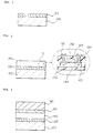
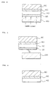
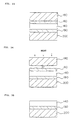
- Figs. 1 to 6 are drawings illustrating a method of transferring a thin film device, which is the premise of the present invention.
- a separation layer (light absorbing layer) 120 is formed on a substrate 100.
- the substrate 100 a substrate having light transmission, which can transmit light, is used.
- the light transmittance is preferably 10% or more, more preferably 50% or more. With too low transmittance, attenuation (loss) of light increases, and thus a larger quantity of light is required for separating the separation layer 120.
- the substrate 100 is preferably made of a material having high reliability, particularly preferably made of a material having excellent heat resistance.
- the reason for this is that for example, in forming a layer 140 to be transferred and an intermediate layer 142, which will be described below, the process temperature is increased (for example, about 350 to 1000C) according to the type and the forming method used, and even in such a case, the ranges of deposition conditions such as a temperature condition and the like set for forming the layer 140 to be transferred on the substrate 100 are widened when the substrate 100 has excellent heat resistance.
- the substrate 100 is preferably made of a material having a strain point of Tmax or more.
- the constituent material of the substrate 100 preferably has a strain point of 350°C or more, more preferably 500°C or more. Examples of such materials include heat-resistant glass such as quartz glass, Corning 7059, Nihon Denki glass 0A-2, and the like.
- the thickness of the substrate 100 is not limited, the thickness is preferably about 0.1 to 5.0 mm, more preferably about 0.5 to 1.5 mm.
- the use of the excessively thin substrate 100 causes deterioration in intensity, while the use of the excessively thick substrate 100 causes attenuation of light with low transmittance. With the substrate 100 having high transmittance, the thickness thereof may be over the upper limit.
- the substrate 100 preferably has a uniform thickness in order to allow uniform irradiation of light.
- the bonding force is decreased or lost by any one or a plurality of actions including physical actions (light, heat, and the like), chemical actions (chemical reaction with a chemical), and mechanical actions (tensile force, vibration, and the like), thus accelerating separation of the substrate 100 through the separation layer 120.
- An example of the separation layer 120 is a layer having the property of absorbing irradiation light to produce separation (referred to as “in-layer separation” and “interface separation” hereinafter) in the layer and/or the interface.
- in-layer separation and “interface separation” hereinafter
- the interatomic or intermolecular bonding force of the constituent material of the separation layer 120 is lost or decreased by irradiation of light, i.e., ablation occurs, resulting in in-layer separation and/or interface separation.
- gases are released from the separation layer 120 by irradiation of light, manifesting the separating effect.
- such cases include cases in which the components contained in the separation layer 120 are released as gases, and cases in which the separation layer 120 absorbs light to momentarily produce gases, which are released to contribute to separation.
- the present invention is characterized in that after the separation layer 120 having the above characteristics is formed, separation accelerating ions are implanted in the separation layer 120, thereby accelerating a separation phenomenon in the separation layer in the subsequent step. Therefore, any types of ions for accelerating separation may be used as long as the separation phenomenon is accelerated by the physical action, the chemical action or the mechanical action.
- composition of the separation layer 120 examples include the following compositions A to E.
- the thickness of the separation layer 120 depends upon various conditions such as the purpose of separation, the composition of the separation layer 120, the layer structure, the forming method, etc., the thickness is preferably about 1 nm to 20 ⁇ m, more preferably about 5 nm to 2 ⁇ m, most preferably 5 nm to 1 ⁇ m.
- the separation layer 120 having a too small thickness causes deterioration in uniformity of deposition, and nonuniformity in separation, while the separation layer 120 having a too large thickness requires high powder (quantity) of light for securing the good separation ability of the separation layer 120, as well as much time for the subsequent work of removing the separation layer 120.
- the thickness of the separation layer is preferably as uniform as possible.
- the method of forming the separation layer 120 is not limited, and is appropriately selected depending upon various conditions such as the film composition, the film thickness, etc.
- the forming method include various vapor phase deposition methods such as CVD (including MOCVD, low-pressure CVD, and ECR-CVD), vapor deposition, molecular beam deposition (MB), sputtering, ion plating, PVD, and the like; various plating methods such as electroplating, dip plating (dipping), electroless plating, and the like; coating methods such as Langmuir-Blodgett's (LB) process, spin coating, spray coating, roll coating, and the like; various printing methods; a transfer method; an ink jet method; a powder jet method; and the like.
- the separation layer 120 can also be formed by a combination of at least two of these methods.
- composition of the separation layer 120 comprises amorphous silicon (a-Si)
- deposition is preferably carried out by CVD, particularly low-pressure CVD or plasma CVD.
- the separation layer 120 is made of ceramic by using a sol-gel method, or an organic polymer material
- deposition is preferably carried out by the coating method, particularly spin coating.
- the layer to be transferred (thin film device layer) 140 is formed on the separation layer 120.
- the process after step 2 will be described in detail later with reference to Figs. 8 to 18, in this embodiment, the step of implanting ions for accelerating separation in the separation layer 120 is carried out in the course of the steps shown in Figs. 8 to 13.
- Fig. 2 also shows an enlarged section of portion K (the portion shown by a one-dot chain line in Fig. 2) of the thin film device layer 140 on the right side thereof.
- the thin film device layer 140 comprises TFT (thin film transistor), for example, formed on a SiO 2 film (intermediate layer) 142, the TFT comprising a source drain layer 146 formed by introducing n-type impurities in a polysilicon layer, a channel layer 144, a gate insulation film 148, a gate electrode 150, an interlayer insulation film 154, and an electrode 152, for example, made of aluminum.
- TFT thin film transistor
- the SiO 2 film As the intermediate layer provided in contact with the separation layer 120, other insulating films such as a Si 3 N 4 film and the like can also be used.
- the thickness of the SiO 2 film (intermediate layer) is appropriately determined according to the purpose of formation, and the degree of the function exhibited, the thickness is preferably about 10 nm to 5 ⁇ m, more preferably about 40 nm to 1 ⁇ m.
- the intermediate layer is formed for various purposes.
- the intermediate layer exhibits at least one of the functions as a protective layer for physically or chemically protecting the layer 140 to be transferred, an insulation layer, a conductive layer, a laser shielding layer, a barrier layer for preventing migration, and a reflecting layer.
- the layer to be transferred (thin film device layer) 140 may be formed directly on the separation layer 120 without the intermediate layer such as the SiO 2 layer or the like formed, according to circumstances.
- the layer 140 to be transferred comprises the thin film device such as TFT or the like, as shown on the right side of Fig. 2.
- examples of the thin film device include a thin film diode; a photoelectric transducer (an optical sensor and a solar cell) and ss silicon resistor element, which comprise PIN junctions of silicon; other thin film semiconductor devices; an electrode (for example, a transparent electrode of ITO of mesa film); a switching element; memory; an actuator such as a piezoelectric element; a micro mirror (piezo thin film ceramic); a magnetic recording thin film head, a coil, an inductor; a filter; a reflecting film, a dichroic mirror, and the like.
- Such a thin film device is generally formed through a relatively high process temperature in relation to the forming method.
- a substrate with high reliability, which can resist the process temperature, is thus required as the substrate 100.
- the thin film device layer 140 is joined (bonded) to a transfer material 180 through an adhesive layer 160.
- the adhesive which constitutes the adhesive layer 160 include various curable adhesives such as reactive curable adhesives; thermal curable adhesives:light curable adhesives such as ultraviolet curable adhesives; and the like; anaerobic curable adhesives, and the like.
- curable adhesives such as reactive curable adhesives; thermal curable adhesives:light curable adhesives such as ultraviolet curable adhesives; and the like; anaerobic curable adhesives, and the like.
- any of epoxy, acrylate and silicone types, and the like may be used.
- the adhesive layer 160 is formed by, for example, a coating method.
- the curable adhesive is coated on the layer to be transferred (thin film device layer) 140, and the transfer material 180 is joined to the adhesive layer which is then cured by a curing method according to the characteristics of the curable adhesive used to bond and fix the layer to be transferred (thin film device layer) 140 and the transfer material 180.
- a light curable adhesive In the case of a light curable adhesive, irradiation of light is effected from the outside of one of the light transmitting substrate 100 and the light transmitting transfer material 180 (or the outsides of both the light transmitting substrate and transfer material).
- a light curable adhesive such as an ultraviolet curable adhesive or the like is preferable, which has little effect on the thin film device layer.
- a water-soluble adhesive can also be used.
- water-soluble adhesives include Chemiseal U-451D (trade name) produced by Chemitech Co., Ltd., Three Bond 3046 (trade name) produced by Three Bond Co., Ltd., and the like.
- an adhesive soluble in various organic solvents can also be used.
- an adhesive exhibiting the separating function by heat can also be used.
- adhesives include Liva Alpha (trade name) produced by Nitto Denko, and the like.
- an adhesive exhibiting the separating function by ultraviolet irradiation can also be used.
- adhesives include Dicing Tape D-210 and D-636 for glass ceramic, which are produced by Lintech Co., Ltd.
- the adhesive layer 160 may be formed on the transfer material 180 side, and the layer to be transferred (thin film device layer) 140 may be bonded to the adhesive layer 160.
- the adhesive layer 160 may be omitted.
- the transfer material 180 is not limited, a substrate (plate material), particularly a transparent substrate, can be used.
- a substrate may be either a flat plate or a curved plate.
- the transfer material 180 may have the characteristic that the heat resistance and abrasion resistance are lower than the substrate 100.
- the reason for this is that in the present invention, the layer to be transferred (thin film device layer) 140 is formed on the substrate 100 side, and then transferred to the transfer material 180, and thus characteristics required for the transfer material 180, particularly heat resistance, do not depend upon the temperature condition and the like in formation of the layer to be transferred (thin film device layer) 140.
- the transfer material 180 comprises a material preferably having a glass transition point (Tg) or softening pint of 800°C or less, more preferably 500°C or less, most preferably 320°C or less.
- the transfer material 180 preferably has some degree of rigidity (strength) as a mechanical characteristic, but it may have flexibility or elasticity.
- Examples of such constituent materials of the transfer material 180 include various synthetic resins and various glass materials. Particularly, various synthetic resins and normal (low-melting-point) inexpensive glass materials are preferably used.
- the synthetic resins may be either thermoplastic resins or thermosetting resins.
- resins include polyolefins such as polyethylene, polypropylene, ethylenepropylene copolymers, ethyl-vinyl acetate copolymers (EVA), and the like; cyclic polyolefins; modified polyolefins; polyvinyl chlorides; polyvinylidene chlorides; polystyrenes; polyamides; polymides; polyamide-imide; polycarbonate; poly-(4-methylpentene-1); ionomers; acrylic resins; polymethyl methacrylate; acryl-styrene copolymers (AB resins); butadiene-styrene copolymers; polyo copolymers (EVOH); polyesters such as polyethylene terephthalate (PET), polybutylene terephthalate (PBT), polycyclohexane terephthalate (PCT), and the like; polyether, polyether
- glass materials examples include silicate glass (quartz glass), alkali silicate glass, soda-lime glass, potash lime glass, lead (alkali) glass, barium glass, borosilicate glass, and the like.
- silicate glass these types of glass desirably have low melting points, and are relatively easy to mold and process and inexpensive, as compared with silicate glass.
- the transfer material 180 made of a synthetic resin the large transfer material 180 can be integrally formed, and a complicated shape having a curved surface or unevenness can easily be produced, with various advantages of low material cost and production cost. Therefore, the use of a synthetic resin is advantageous for producing an inexpensive large device (for example, a liquid crystal display).
- the transfer material 180 may constitute an independent device by itself, for example, such as a liquid crystal cell, or constitute a portion of a device, for example, such as a color filter, an electrode layer, a dielectric layer, an insulation layer, or a semiconductor device.
- the transfer material 180 may comprise a material such as a metal, ceramic, a stone, wood paper, or the like, or any desired surface (the surface of a watch, an air conditioner, a printed board, or the like) which constitutes an article, or a surface of a structure, such as a wall, a column, a ceiling, window glass, or the like.
- the substrate 100 is irradiated by light from the rear side thereof.
- the separation layer 120 is irradiated by the light. As a result, in-layer separation and/or interface separation occurs in the separation layer 120 to decrease or lose bonding force.
- the principle of the occurrence of in-layer separation and/or interface separation in the separation layer 120 possibly lies in the fact that ablation occurs in the constituent material of the separation layer 120, the gases contained in the separation layer 120 are discharged, and a phase change such as melting, transpiration, or the like occurs immediately after irradiation.
- the ablation means that the fixed material (the constituent material of the separation layer 120) which absorbs irradiation light is chemically or thermally excited to cut the atomic bonds or molecular bonds in the surface or inside of the separation layer 120, releasing atoms or molecules.
- the ablation mainly occurs as a phenomenon in that a phase change such as melting, transpiration (evaporation) or the like occurs over the entire constituent material of the separation layer 120 or in a portion thereof. In some cases, the phase change causes a fine foam state to deteriorate the bonding force.
- the separation layer 120 produces the in-layer separation or interface separation or both depends upon the composition of the separation layer 120 and other various factors. Examples of the factors include conditions such as the type, wavelength, strength, reach depth of the irradiation light, etc.
- separation accelerating ions are implanted in the separation layer 120 in order to securely produce the separation phenomenon.
- the separation accelerating ions have at least one or a combination of at least two of the three functions below, and accelerate the separation phenomenon of the separation layer 120 in the fourth step.
- One of the functions is to gasify the separation accelerating ions of, for example, hydrogen (H) or nitrogen (N), implanted in the separation layer 120, thereby accelerating separation of the separation layer 120 in the fourth step.
- H hydrogen
- N nitrogen
- Another function is to cut bonds of atoms or molecules, which constitute the separation layer 120, by the separation accelerating ions of, for example, hydrogen (H), nitrogen (N) or silicon (Si) to previously damage the separation layer 120 in the step of implanting the separation accelerating ions. Therefore, the previously damaged separation layer 120 is relatively easily separated in the fourth step.
- H hydrogen
- N nitrogen
- Si silicon
- the other function is to change the characteristics of the separation layer 120 by the separation accelerating ions of, for example, hydrogen (H), nitrogen (N) or silicon (Si) to previously decrease adhesion between the separation layer 120 and the substrate 100 in the step of implanting the separation accelerating ions. Therefore, the separation layer 120 with decreased adhesion to the substrate is relatively easily separated in the fourth step.
- the separation accelerating ions of, for example, hydrogen (H), nitrogen (N) or silicon (Si)
- any light may be used as long as it produces in-layer separation and/or interface separation in the separation layer 120.
- Examples of such light include X-rays, ultraviolet rays, visible light, infrared rays (heat rays), laser beams, millimeter waves, micro waves, electron beams, radiation ( ⁇ -rays, ⁇ -rays, ⁇ -rays), and the like.
- a laser beam is preferable in the point that it readily causes separation (ablation) in the separation layer 120.
- a laser device for emitting the laser beam various gas lasers, solid lasers (semiconductor lasers), and the like can be used.
- An excimer laser, an Nd-YAG laser, an Ar laser, a CO 2 laser, a CO laser, a He-Ne laser and the like are preferably used, and an excimer laser is particularly preferred.
- the excimer laser Since the excimer laser outputs high energy in the short wavelength region, it can produce ablation in the separation layer 120 within a very short time, and can separate the separation layer 120 without substantially no temperature rise in the adjacent transfer material 180 and substrate 100, i.e., without deterioration and damage.
- the wavelength of the irradiating laser beam is preferably about 100 nm to 350 nm.
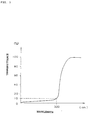
- Fig. 7 shows an example of transmittance of the substrate 100 relative to the wavelength of light.
- the substrate 100 has the property that transmittance rapidly increases at a wavelength of 300 nm.
- the substrate 100 is irradiated with light at a wavelength of 210 nm or more, for example, Xe-Cl excimer laser light (wavelength 308 nm), KrF laser light (wavelength 248 nm), or the like.
- the wavelength of the irradiation laser light is preferably about 350 to 1200 nm.
- the energy density of the irradiation laser beam is preferably about 10 to 5000 mJ/cm 2 , more preferably about 100 to 500 mJ/cm 2 .
- the irradiation time is preferably about 1 to 1000 nsec, and more preferably about 10 to 100 nsec. With a low energy density or a short irradiation time, ablation does not sufficiently occur, while with a high energy density or a long irradiation time, the irradiation light transmitted through the separation layer 120 possibly adversely affects the layer 140 to be transferred.
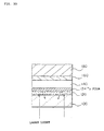
- a method is used in which a metallic film 124 of tantalum (Ta) or the like is formed on the separation layer (laser absorbing layer) 120, for example, as shown in Fig. 30. This causes the laser light transmitted through the separation layer 120 to be completely reflected by the interface with the metallic film 124, thereby preventing adverse effects on the thin film device formed above the metallic film 124.
- Ta tantalum
- force is applied to the substrate 100 to separate the substrate 100 from the separation layer 120.
- the separation layer sometimes adheres to the substrate 100 after separation.
- the residue of the separation layer 120 is removed by a method of washing, etching, ashing, polishing, or the like, or a method comprising a combination thereof.
- the layer to be transferred (thin film device layer) 140 is transferred to the transfer material 180.
- the substrate 100 When a part of the separation layer adheres to the separated substrate 100, it is removed by the same method.
- the substrate 100 made of an expensive material such as quartz glass, or a rare material, the substrate 100 is preferably reused (recycled). Namely, the present invention can also be applied to the substrate 100 desired to be reused, with high availability.
- the layer to be transferred (thin film device layer) 140 is completely transferred to the transfer material 180 through the above-described steps. Then, it is also possible to remove a SiO 2 film adjacent to the layer to be transferred (thin film device layer) 140, and form a conductive layer such as wiring and a desired protective film on the layer 140 to be transferred.
- the layer to be transferred (thin film device layer) 140 as an object to be separated is separated by using the separation layer joined to the layer transferred (thin film device layer) 140, not separated directly. Therefore, the object to be separated (the layer 140 to be transferred) can be readily, securely, and uniformly separated (transferred) regardless of the characteristics and conditions of the object to be separated (the layer 140 to be transferred), without damaging the object to be separated (the layer 140 to be transferred) in the separating operation. Thus, the high reliability of the layer 140 to be transferred can be maintained.
- CMOS structure TFT is formed as the thin film device layer 140 on the substrate 100 and the separation layer 120, with reference to Figs. 8 to 18. Description will be also made of the step of implanting the separation accelerating ions in the course of this process.
- a separation layer for example, an amorphous silicon layer formed by the LPCVD method 120, an intermediate layer (for example, a SiO 2 film) 142, and an amorphous silicon layer (for example, formed by the LPCVD method) 143 are laminated in turn on a transmitting substrate (for example, a quartz substrate) 100, and then the entire surface of the amorphous silicon layer 413 is irradiated with a laser beam from above to anneal it. As a result, the amorphous silicon layer 143 is recrystallized to form a polysilicon layer.
- a transmitting substrate for example, a quartz substrate
- the same position is preferably irradiated with light at least twice so that the beam centers are overlapped with each other (except Gaussian beams). This is because the amorphous silicon layer 143 can be sufficiently recrystallized by multiple irradiation without problems such as light leakage.
- the step of implanting the separation accelerating ions is preferably carried out at an execution time after the formation of the separation layer and before the laser annealing step for recrystallization because the ions can be implanted without the need for a mask.
- the execution time is any one of the following:
- the step of implanting the separation accelerating ions can be carried out by using a known ion implantation apparatus. Namely, for example, when hydrogen ions are implanted, gas plasma containing hydrogen is formed, and the produced hydrogen ions are accelerated by an electric field to be implanted in the separation layer 120.
- the ion implantation step may be carried out at execution time (D) after laser annealing.
- the ions can be implanted with the channel region masked, without deteriorating transistor characteristics.
- the mask is removed after the ion implantation step.
- the polysilicon layer obtained by laser annealing is patterned to form islands 144a and 144b as a channel pattern.
- the step of implanting the separation accelerating ions can also be carried out at execution time (E) after the second step (the step of forming the channel pattern).
- execution time (E) the step of forming the channel pattern.
- a micro pattern 201 is previously formed on portions of the islands 144a and 144b, which are opposite to the channel regions in the islands 144a and 144b.
- the separation accelerating ions for example, hydrogen ions
- the mask pattern 201 is removed.
- gate insulation films 148a and 148b are formed by, for example, the CVD method to cover the islands 144a and 144b, respectively.
- the step of implanting the separation accelerating ions can also be carried out at execution time (F) after the third step (gate insulation film).
- a mask pattern 202 is preferably previously formed on portions of the gate insulation films 148a and 148b, which are opposite to the channel regions in the islands 144a and 144b.
- gate electrodes 150a and 150b made of polysilicon or a metal are formed.
- a mask layer 170 made of polyimide or the like is formed for implanting, for example, boron (B) ions, in self alignment by using the gate electrode 150b and the mask layer 170 as a mask. As a result, p + layers 172a and 172b are formed.
- the step of implanting the separation accelerating ions can also be carried out at execution time (G) at the same time as the boron ion implanting step.
- execution time (G) plasma of a gas mixture of B 2 H 6 (5%) + H 2 (95%) is formed, and the produced boron ions and hydrogen ions are accelerated to be introduced into the substrate through a mass analyzer.
- boron ions having higher mass are stopped in the polycrystalline silicon layer on the upper layer side, while hydrogen ions having lower mass are implanted deep and reach the separation layer 120.
- the gate electrode 150b functions as the same as the mask pattern 201 shown in Fig. 31 or the mask pattern 202 shown in Fig. 32, a mask layer can be further provided on the gate electrode 150b according to the acceleration voltage.
- a mask layer 174 made of polyimide or the like is formed for implanting, for example, phosphorus (P) ions, in self alignment by using the gate electrode 150a and the mask layer 174 as a mask. As a result, n + layers 146a and 146b are formed.
- the step of implanting the separation accelerating ions can also be carried out at execution time (H) at the same time as the phosphorus ion implanting step.
- execution time (H) at the same time as the phosphorus ion implanting step.
- plasma of a gas mixture of PH 3 (5%) + H 2 (95%) is formed, and the produced phosphorus ions and hydrogen ions are accelerated to be introduced into the substrate through a mass analyzer.
- phosphorus ions having higher mass are stopped in the polycrystalline silicon layer on the upper layer side, while hydrogen ions having lower mass are implanted deep and reach the separation layer 120.
- the gate electrode 150a functions as the same as the mask pattern 201 shown in Fig. 31 or the mask pattern 202 shown in Fig. 32, a mask layer can be further provided on the gate electrode 150a according to the acceleration voltage.
- the execution times (G) and (H) of the step of implanting the separation accelerating ions are the same as the steps of implanting impurity ions in the source and drain regions in the steps 5 and 6, respectively. However, the step of implanting the separation accelerating ions may be separately carried out before or after the steps 5 and 6.
- an interlayer insulation film 154 is formed, contact holes are selectively formed, and then electrodes 152a to 152d are formed.
- CMOS structure TFT corresponds to the layer to be transferred (thin film device layer) 140 shown in Figs. 2 to 6.
- a protective film may also be formed on the interlayer insulation film 154.
- an epoxy resin layer 160 is formed as an adhesive layer on the CMOS structure TFT, and the TFT is bonded to the transfer material (for example, a soda glass substrate) 180 through the epoxy resin layer 160. Then, the epoxy resin is cured by heating to bond (join) the transfer material 180 and the TFT.
- the adhesive layer 160 may be made of a photopolymer resin which is an ultraviolet curable adhesive. In this case, the polymer is cured by ultraviolet irradiation from the transfer material 180 side, not by heating.
- the transmitting substrate 100 is irradiated with, for example, Xe-Cl excimer laser light from the rear side thereof. This causes separation in the separation layer 120 and/or the interface thereof.
- the substrate 100 is peeled.
- the separation layer 120 is removed by etching. Consequently, as shown in Fig. 18, the CMOS structure TFT is transferred to the transfer material 180.
- a layer 140 to be transferred which comprises a thin film device layer, is transferred twice, and thus the steps shown in Figs. 33 to 35 are added to the steps of the first embodiment shown in Figs. 1 to 6.
- the separation layer 120 shown in Figs. 2 to 5 are referred to as a "first separation layer”.
- the adhesive layer 160 shown in Figs. 3 to 6 is also referred to as a "second separation layer”.
- the transfer material 180 shown in Figs. 3 to 6 is referred to as a "primary transfer material”. Therefore, in the second embodiment, the layer 140 to be transferred is transferred to the primary transfer material 180 through the second separation layer 160 after the step shown in Fig. 6 is completed.
- a heat melting adhesive As the material of the second separation layer 160 , a heat melting adhesive, a water-soluble adhesive and the same materials as the first separation layer 120 can be used. In this case, in order to facilitate separation with the second separation layer 160, the ion implantation described above in the first embodiment can be carried out.
- a secondary transfer layer 200 is bonded to the lower side (the exposed surface) of the thin film device layer 140 through an adhesive layer 190.
- the adhesive which constitutes the adhesive layer 190 include various curable adhesives such as reactive curable adhesives; thermal curable adhesives; light curable adhesives such as ultraviolet curable adhesives, and the like; anaerobic curable adhesives, and the like.
- curable adhesives such as reactive curable adhesives; thermal curable adhesives; light curable adhesives such as ultraviolet curable adhesives, and the like; anaerobic curable adhesives, and the like.
- any of epoxy, acrylate and silicone types, and the like may be used.
- the adhesive layer 190 is formed by, for example, the coating method.
- the curable adhesive is coated on the lower side of the layer to be transferred (thin film device layer) 140, and the secondary transfer material 200 is joined to the adhesive layer which is then cured by a curing method according to the characteristics of the curable adhesive used to bond and fix the layer to be transferred (thin film device layer) 140 and the secondary transfer material 200.
- irradiation of light is preferably effected from the outside of the light transmitting secondary transfer material 200.
- a light curable adhesive such as an ultraviolet curable adhesive or the like, which having little effect on the thin film device layer, is used as the adhesive
- light irradiation may be effected from the light transmitting primary transfer material 180 side or both sides of the light transmitting primary and the secondary transfer materials 180 and 200.
- the adhesive layer 190 may be formed on the secondary transfer material 200 side, and the layer to be transferred (thin film device layer) 140 may be bonded thereto.
- the adhesive layer 190 may be omitted.
- the secondary transfer material 200 is not limited, a substrate (plate material), particularly a transparent substrate, can be used.
- a substrate may be either a flat plate or a curved plate.
- the secondary transfer material 200 may have the characteristic that the heat resistance and abrasion resistance are lower than the substrate 100.
- the reason for this is that in the present invention, the layer to be transferred (thin film device layer) 140 is formed on the substrate 100 side, and then transferred to the secondary transfer material 200, and thus characteristics required for the secondary transfer material 200, particularly heat resistance, do not depend upon the temperature condition and the like in formation of the layer to be transferred (thin film device layer) 140. This point is true for the primary transfer material 180.
- each of the primary and secondary transfer materials 180 and 200 comprises a material preferably having a glass transition point (Tg) or softening pint of 800°C or less, more preferably 500°C or less, most preferably 320°C or less.
- the primary and secondary transfer materials 180 and 200 preferably have some degree of rigidity (strength) as a mechanical characteristic, but both materials may have flexibility or elasticity.
- Examples of such constituent materials of the primary and secondary transfer materials 180 and 200 include various synthetic resins and various glass materials. Particularly, various synthetic resins and ordinary (low-melting-point) inexpensive glass materials are preferably used.
- the synthetic resins may be either thermoplastic resins or thermosetting resins.
- resins include polyolefins such as polyethylene, polypropylene, ethylenepropylene copolymers, ethyl-vinyl acetate copolymers (EVA), and the like; cyclic polyolefins; modified polyolefins; polyvinyl chlorides; polyvinylidene chlorides; polystyrenes; polyamides; polymides; polyamide-imide; polycarbonate; poly-(4-methylpentene-1); ionomers; acrylic resins; polymethyl methacrylate; acryl-styrene copolymers (AB resins); butadiene-styrene copolymers; polyo copolymers (EVOH); polyesters such as polyethylene terephthalate (PET), polybutylene terephthalate (PBT), polycyclohexane terephthalate (PCT), and the like; polyether, polyether
- glass materials examples include silicate glass (quartz glass), alkali silicate glass, soda-lime glass, potash lime glass, lead (alkali) glass, barium glass, borosilicate glass, and the like.
- silicate glass these types of glass desirably have low melting points, and are relatively easy to mold and process and inexpensive, as compared with silicate glass.
- the large secondary transfer material 200 can be integrally formed, and a complicated shape having a curved surface or unevenness can easily be produced, with various advantages of low material cost and production cost. Therefore, the use of a synthetic resin is advantageous for producing an inexpensive large device (for example, a liquid crystal display).
- the secondary transfer material 200 may constitute an independent device by itself, for example, such as a liquid crystal cell, or constitute a portion of a device, for example, such as a color filter, an electrode layer, a dielectric layer, an insulation layer, or a semiconductor device.
- each of the primary and secondary transfer materials 180 and 200 may comprise a material such as a metal, ceramic, a stone, wood paper, or the like, or any desired surface (the surface of a watch, an air conditioner, a printed board, or the like) which constitutes an article, or a surface of a structure such as a wall, a column, a ceiling, window glass, or the like.
- a heat-melting adhesive layer 160 as a second separation layer is heat-melted by heating.
- the adhesive force of the heat-melting adhesive layer 160 is weakened, enabling separation of the primary transfer material 180 from the thin film device layer 140.
- the heat-melting adhesive which adheres to the primary transfer material 180 is removed for permitting repeated reuse of the primary transfer material 180.
- a region including at least the second adhesive layer 160 may be brought into contact with water, and preferably dipped in pure water.
- a region including at least the second adhesive layer 160 may be brought into contact with an organic solvent.
- a region including at least the second adhesive layer 160 may be heated or irradiated with ultraviolet rays through another layer.
- an ablation layer as the second separation layer, like the first separation layer 120, the separation phenomenon is produced in the secondary separation layer by light irradiation. At this time, separation is accelerated by the effect of implanted ions.
- the second separation layer 160 which adheres to the surface of the thin film device 140 is removed to obtain the thin film device layer 140 transferred to the secondary transfer material 200, as shown in Fig. 35.
- the laminate relation of the thin film device layer 140 to the primary transfer material 200 is the same as the initial laminate relation of the thin film device layer 140 to the substrate 100 shown in Fig. 2.
- the layer to be transferred (thin film device layer) 140 is completely transferred to the secondary transfer material 200 through the above-mentioned steps. Then, a SiO 2 film adjacent to the layer to be transferred (thin film device layer) 140 may be removed, or a conductive film such as wiring or the like and a desired protective film may be formed on the layer 140 to be transferred.
- the layer to be transferred (thin film device layer) 140 serving as an object to be separated is separated at the first separation layer 120 and the second separation layer 160 and transferred to the secondary transfer material 200, not separated directly.
- the object to be separated (the layer 140 to be transferred) can readily, securely and uniformly be transferred regardless of the characteristics and conditions of the layer 140 to be transferred, without damaging the object to be separated (the layer 140 to be transferred) in the separating operation, thereby maintaining the high reliability of the layer 140 to be transferred.
- a microcomputer comprising a thin film device can be formed on a desired substrate, for example, as shown in Fig. 19(a).
- CPU 300, RAM 320, and an input/output circuit 360 each of which comprises a circuit formed by using a thin film device, and a solar cell 340 comprising an amorphous silicon PIN junction for supplying a source voltage to these circuits are mounted on a flexible substrate 182 comprising plastic or the like.
- the microcomputer shown in Fig. 19(a) is formed on the flexible substrate, and thus has the properties that it is strong against bending, as shown in Fig. 19(b), and against falling because of its light weight.
- an active matrix liquid crystal display device comprises an illumination light source 400 such as a back light, a polarizer 420, an active matrix substrate 440, a liquid crystal 460, a counter substrate 480, and a polarizer 500.
- the active matrix substrate 440 and the counter substrate 480 of the present invention When a flexible substrate such as a plastic film or the like is used as the active matrix substrate 440 and the counter substrate 480 of the present invention, by using a reflecting plate in place of the illumination light source 400 to form a reflective liquid crystal panel, it is possible to realize an active matrix liquid crystal panel having flexibility, impact resistance and light weight.
- the formation of pixel electrodes made of a metal makes the reflecting plate and the polarizer 420 unnecessary.
- the active matrix substrate 440 used in this embodiment is an active matrix substrate with a built-in driver in which TFTs are arranged in a pixel region 442, and a driver circuit (a scanning line driver and a data line driver) 444 is mounted on the substrate.
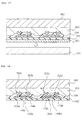
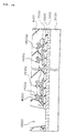
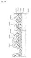
- Fig. 21 is a sectional view showing a principal portion of the active matrix liquid crystal display device
- Fig. 22 is a drawing showing the circuit configuration of the principal portion of the liquid crystal display device.
- the pixel region 442 comprises the liquid crystal 460 and TFT (M1) which includes a gate connected to a gate line G1, and source and drain one of which is connected to a data line D1, the other being connected to the liquid crystal 460.
- TFT TFT
- the driver region 444 comprises TFT (M2) formed by the same process as TFT (M1) of the pixel region.
- TFT (M1) of the pixel region 442 comprises source and drain layers 1100a and 1100b, a channel 1100e, a gate insulation film 1200a, a gate electrode 1300a, an insulation film 1500, and source and drain electrodes 1400a and 1400b.
- Reference numeral 1700 denotes a pixel electrode
- reference numeral 1702 denotes a region (a voltage applying region for the liquid crystal) where a voltage is applied to the liquid crystal from the pixel electrode 1700.
- an alignment film is omitted.
- the pixel electrode 1700 is made of ITO (in the case of a transmissive liquid crystal panel) or a metal (in the case of a reflective liquid crystal panel) such as aluminum.
- an under insulation film (intermediate layer) 1000 below the pixel electrode 1700 is completely removed from the voltage applying region 1702 for the liquid crystal, the configuration is not necessarily limited to this, and the under insulation film (intermediate layer) 1000 may be left when it is thin and does not interfere with voltage application to the liquid crystal.
- TFT (M2) which constitutes the driver region 444 comprises source and drain layers 1100c and 1100d, a channel 1100f, a gate insulation film 1200b, a gate electrode 1300b, an insulation film 1500 and source and drain electrodes 1400c and 1400d.
- reference numeral 480 denotes, for example, a counter substrate (for example, a soda glass substrate), and reference numeral 482 denotes a common electrode.
- Reference numeral 1000 denotes a SiO 2 film
- reference numeral 1600 denotes an interlayer insulation film (for example, a SiO 2 film)
- reference numeral 1800 denotes an adhesive layer.
- Reference numeral 1900 denotes a substrate (transfer material) comprising, for example, a soda glass substrate.
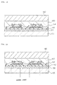
- the TFTs (M1 and M2) shown in Fig. 23 are formed on a substrate (for example, a quartz substrate) 3000 with high reliability, which transmits laser beams, through the same production process as shown in Figs. 8 to 18, and the protective film 1600 is then formed.
- reference numeral 3100 denotes a separation layer (laser absorbing layer) in which the separation accelerating ions are implanted.
- both TFTs (M1 and M2) are n-type MOSFET.
- TFT is not limited to this, and it may be either p-type MOSFET or CMOS structure TFT.
- the protective film 1600 and the under insulation film 1000 are selectively etched to selectively form apertures 4000 and 4200.
- the two apertures are simultaneously formed by using a common etching step.
- the under insulation film (intermediate layer) 1000 is completely removed from the aperture 4200, the configuration is not limited to this, and the under insulation film (intermediate layer) 1000 may be left when it is thin and does not interfere with voltage application to the liquid crystal.
- the pixel electrode 1700 made of an ITO film or a metal such as aluminum is formed.
- a transmissive liquid crystal panel and a reflective liquid crystal panel, respectively are formed.
- the substrate 1900 is joined (bonded) through the adhesive layer 1800.
- the substrate 3000 is irradiated with excimer laser light from the rear side thereof to produce the separation phenomenon in the separation layer 3100 by using the action of the separation accelerating ions. Then, the substrate 3000 is peeled. At this time, only a little force is required for peeling the substrate 3000 without mechanical damage to the TFT.
- the separation layer (laser absorbing layer) 3100 is removed.
- the active matrix substrate 440 is completed, as shown in Fig. 27.
- the bottom (the region denoted by reference numeral 1702) of the pixel electrode 1700 is exposed to permit electric connection with the liquid crystal.
- the alignment film is formed on the surface of the insulation film (the intermediate film of SiO 2 ) 1000 and the surface of the pixel electrode 1700 of the active matrix substrate 440, followed by alignment processing. In Fig. 27, the alignment film is omitted.
- the active matrix substrate 440 shown in Fig. 21 and the counter substrate 480 in which the common electrode is formed on the surface thereof opposite to the pixel electrode1700, and the surface is subjected to alignment processing are sealed with a sealant (a sealing material), and the liquid crystal is sealed in the space between both substrates to complete the liquid crystal display device shown in Fig. 21.
- a sealant a sealing material
- Fig. 28 shows a fifth embodiment of the present invention.
- the above-described method of transferring a thin film device is carried out a plurality of times to transfer a plurality of patterns including a thin film device onto a substrate (transfer material) larger than the initial substrate, finally forming a large scale active matrix substrate.
- pixel regions 7100a to 7100P transfer to a large substrate 7000 is executed a plurality of times to form pixel regions 7100a to 7100P.
- TFT and wiring are formed, as shown by a one-dot chain line in the upper portion of Fig. 28.
- reference numeral 7210 denotes a scanning line; reference numeral 7200, a signal line; reference numeral 7220, a gate electrode; reference numeral 7230, a pixel electrode.
- a thin film pattern can be transferred a plurality of times by repeatedly using a substrate with high reliability or a plurality of first substrates to form a large scale active matrix substrate on which thin film devices with high reliability are mounted.
- Fig. 29 shows a sixth embodiment of the present invention.
- This embodiment is characterized in that the above-described method of transferring a thin film device is performed a plurality of times to transfer a plurality of patterns including thin film devices (namely, thin film devices having different minimum line widths) having different design rules (namely, design rules for pattern design) onto a substrate larger than the original substrate.
- thin film devices namely, thin film devices having different minimum line widths
- design rules namely, design rules for pattern design
- driver circuits (8000 to 8032) formed by a production process finer than the pixel regions (7100a to 7100p) are formed in the periphery of a substrate 6000 by a plurality of times of transfer.
- TFT of the driver circuits can be made finer than the pixel TFT to achieve high integration.
- sampling means (the thin film transistor M2 shown in Fig. 22) for sampling a data signal by controlling a shift register requires high voltage resistance, and thus may be formed by the same process on the same design rule as the pixel TFT.
- a quartz substrate (softening point: 1630°C, strain point: 1070°C, transmittance for excimer laser: about 100%) of 50 mm long x 50 mm wide x 1.1 mm thick was prepared, and an amorphous silicon (a-Si) film was formed as a separation layer (laser absorbing layer) on one side of the quartz substrate by the low-pressure CVD method (Si 2 H 6 gas, 425°C). The thickness of the separation layer was 100 nm.
- a SiO 2 film was formed as an intermediate layer by the ECR-CVD method (SiH 4 + O 2 gas, 425°C) on the separation layer.
- the thickness of the intermediate layer was 200 nm.
- an amorphous silicon film having a thickness of 50 nm was formed as a layer to be transferred on the intermediate layer by the low-pressure CVD method (Si 2 H 6 gas, 425°C), and then crystallized by irradiation of laser light (wavelength 308 nm) to form a polysilicon film. Then, the polysilicon film was subjected to predetermined patterning to form regions serving as source, drain and channel of a thin film transistor.
- a gate insulation film SiO 2 of 1200 nm was formed by the TEOS-CVD method (SiH 4 + O 2 gas), and a gate electrode (a structure in which a high-melting-point metal such as Mo or the like was laminated on polysilicon) was formed on the gate insulation film, followed by ion implantation using the gate electrode as a mask to form source and drain regions in self alignment, forming a thin film transistor.
- hydrogen ions were implanted in the separation layer.
- an electrode and wiring which are connected to the source and drain regions, and wiring connected to the gate electrode are formed according to demand.
- these electrodes and wiring are made of Al, the material is not limited to this.
- an ultraviolet curable adhesive (thickness: 100 ⁇ m) was coated on the thin film transistor, and a large transparent glass substrate (soda glass, softening point: 740°C, strain point: 511°C) of 200 mm long x 300 mm wide x 1.1 mm thick was joined as a transfer material to the coating. Then, the adhesive was cured by ultraviolet irradiation from the glass substrate side to bond and fix the glass substrate.
- beam scan is carried out by irradiation of Xe-Xl excimer laser (wavelength: 308 nm) from the quartz substrate side to produce separation (in-layer separation and interface separation) in the separation layer, as shown in Figs. 31 to 35.
- the energy density of the irradiating Xe-Cl excimer laser was 250 mL/cm 2 , and the irradiation time was 20 nsec.
- the excimer laser irradiation includes spot beam irradiation and line beam irradiation.
- a predetermined unit region for example, 8 mm x 8 mm
- the spot irradiation was continued by beam scanning so that the irradiation regions do not overlap each other (do not overlap in the longitudinal and lateral directions).
- a predetermined unit region for example, 378 mm x 0.1 mm or 378 mm x 0.3 mm (the region where 90% or more of energy can be obtained)
- the quartz substrate was separated from the glass substrate (transfer material) at the separation layer to transfer the thin film transistor and the intermediate layer formed on the quartz substrate to the glass substrate side.
- the quartz substrate was processed by the same method and then reused.
- the transfer from the quartz substrate to the glass substrate of this example can be repeatedly carried out for different plane regions to form more thin film transistors on the glass substrate than the thin film transistors which can be formed on the quartz substrate.
- thin film transistors can be laminated on the glass substrate to form more thin film transistors.
- Example 2 The same transfer of a thin film transistor as Example 1 was repeated except that the separation layer comprised an amorphous silicon film containing 20 at% of H (hydrogen) and formed by the separation layer forming process.
- the separation layer comprised an amorphous silicon film containing 20 at% of H (hydrogen) and formed by the separation layer forming process.
- the H content of the amorphous silicon film was adjusted by appropriately setting deposition conditions of the low-pressure CVD method.
- Example 2 The same transfer of a thin film transistor as Example 1 was repeated except that the separation layer comprised a ceramic thin film (composition: PbTiO 3 , thickness: 200 nm) formed by the sol-gel method using spin coating.
- a ceramic thin film composition: PbTiO 3 , thickness: 200 nm
- Example 2 The same transfer of a thin film transistor as Example 1 was repeated except that the separation layer comprised a ceramic thin film (composition: BaTiO 3 , thickness: 400 nm) formed by sputtering.
- the separation layer comprised a ceramic thin film (composition: BaTiO 3 , thickness: 400 nm) formed by sputtering.
- Example 2 The same transfer of a thin film transistor as Example 1 was repeated except that the separation layer comprised a ceramic thin film (composition: Pb(Zr, Ti)O 3 (PZT), thickness: 50 nm) formed by the laser ablation method.
- the separation layer comprised a ceramic thin film (composition: Pb(Zr, Ti)O 3 (PZT), thickness: 50 nm) formed by the laser ablation method.
- Example 2 The same transfer of a thin film transistor as Example 1 was repeated except that the separation layer comprised a polyimide film (thickness: 200 nm) formed by spin coating.
- the separation layer comprised a polyimide film (thickness: 200 nm) formed by spin coating.
- Example 2 The same transfer of a thin film transistor as Example 1 was repeated except that the separation layer comprised a polyphenylene sulfide film (thickness: 200 nm) formed by spin coating.
- the separation layer comprised a polyphenylene sulfide film (thickness: 200 nm) formed by spin coating.
- Example 2 The same transfer of a thin film transistor as Example 1 was repeated except that the separation layer comprised an A1 film (thickness: 300 nm) formed by sputtering.
- Example 2 The same transfer of a thin film transistor as Example 2 was repeated except that Kr-F excimer laser (wavelength: 248 nm) was used as irradiating light.
- the energy density of the irradiating light was 250 mJ/cm 2 , and the irradiation time was 20 nsec.
- Example 2 The same transfer of a thin film transistor as Example 2 was repeated except that Nd-YAIG laser (wavelength: 1068 nm) was used as irradiating light.
- the energy density of the irradiating light was 400 mJ/cm 2 , and the irradiation time was 20 nsec.
- Example 2 The same transfer of a thin film transistor as Example 1 was repeated except that a thin film transistor comprising a polysilicon film (thickness 80 nm) formed by a high temperature process at 1000°C was used as a layer to be transferred.
- a thin film transistor comprising a polysilicon film (thickness 80 nm) formed by a high temperature process at 1000°C was used as a layer to be transferred.
- Example 2 The same transfer of a thin film transistor as Example 1 was repeated except that a transparent substrate made of polycarbonate (glass transition point: 130°C) was used as a transfer material.
- a transparent substrate made of polycarbonate glass transition point: 130°C
- Example 2 The same transfer of a thin film transistor as Example 2 was repeated except that a transparent substrate made of an AS resin (glass transition point: 70 to 90°C) was used as a transfer material.
- a transparent substrate made of an AS resin glass transition point: 70 to 90°C
- Example 3 The same transfer of a thin film transistor as Example 3 was repeated except that a transparent substrate made of polymethyl methacrylate (glass transition point: 70 to 90°C) was used as a transfer material.
- a transparent substrate made of polymethyl methacrylate glass transition point: 70 to 90°C
- Example 5 The same transfer of a thin film transistor as Example 5 was repeated except that a transparent substrate made of polyethylene terephthalate (glass transition point: 67°C) was used as a transfer material.
- a transparent substrate made of polyethylene terephthalate glass transition point: 67°C
- Example 6 The same transfer of a thin film transistor as Example 6 was repeated except that a transparent substrate made of high-density polyethylene (glass transition point: 77 to 90°C) was used as a transfer material.
- a transparent substrate made of high-density polyethylene glass transition point: 77 to 90°C
- Example 9 The same transfer of a thin film transistor as Example 9 was repeated except that a transparent substrate made of polyamide (glass transition point: 145°C) was used as a transfer material.
- Example 10 The same transfer of a thin film transistor as Example 10 was repeated except that a transparent substrate made of an epoxy resin (glass transition point: 120°C) was used as a transfer material.
- a transparent substrate made of an epoxy resin glass transition point: 120°C
- Example 11 The same transfer of a thin film transistor as Example 11 was repeated except that a transparent substrate made of polymethyl methacrylate (glass transition point: 70 to 90°C) was used as a transfer material.
- a transparent substrate made of polymethyl methacrylate glass transition point: 70 to 90°C
- the use of the transfer technique of the present invention enables transfer of a thin film device (a layer to be transferred) to various transfer materials, particularly enables separation of a substrate required for transfer without the action of excessive force. Therefore, a thin film can be formed, by transfer, on objects made of a material on which a thin film cannot be formed directly or which is unsuitable for forming a thin film, a material easy to mold, an inexpensive material, and the like, and a large object which is difficult to move.
- a transfer material materials having the characteristic that the heat resistance and abrasion resistance are lower than the substrate material, such as various synthetic resins and low-melting-point glass materials, can be used. Therefore, for example, in manufacturing a liquid crystal display comprising thin film transistors (particularly, polysilicon TFT) formed on a transparent substrate, a quartz substrate having excellent heat resistance can be used as the substrate, and an inexpensive transparent substrate easy to process, such as various synthetic resins and low-melting-point glass materials, can be used as the transfer material, thereby readily producing a large inexpensive liquid crystal display. Such an advantage applies to manufacture of a liquid crystal display as well as other devices.
- a layer to be transferred such as a functional thin film
- a substrate having high reliability particularly a substrate having high heat resistance, such as a quartz glass substrate, and then patterned, and thus a functional film having high reliability can be formed on a transfer material regardless of the characteristics of the transfer material.
- thin film devices include a thin film diode, a photoelectric transducer (optical sensor and solar cell) and a silicon resistor element, which comprise a PIN junction of silicon, other thin film semiconductor devices, an electrode (for example, a transparent electrode made of ITO or mesa film), a switching element, memory, an actuator such as a piezoelectric element, a micro mirror (piezo thin film ceramics), a magnetic recording thin film head, a coil, an inductor, a thin film high permeability material and a micro magnetic device comprising a combination thereof, a filter, a reflecting film, a dichroic mirror, and the like.
- the present invention can also applied to liquid crystal display devices regardless of the display mode, i.e., the reflective or transmissive display mode.
- the present invention can be applied to not only a liquid crystal display device for displaying characters and images but also a liquid crystal device comprising a liquid crystal panel functioning as a light valve.
Landscapes
- Thin Film Transistor (AREA)
- Liquid Crystal (AREA)
- Recrystallisation Techniques (AREA)
Abstract
Description
wherein an ion implantation step of implanting ions into the separation layer is provided before the third step.
- 100
- substrate
- 120
- separation layer
- 140
- thin film device layer
- 160
- adhesive layer
- 180
- transfer material
Claims (18)
- A method of separating a thin film device comprising:the first step of forming a separation layer on a substrate;the second step of forming a thin film device on the separation layer; andthe third step of producing a separation phenomenon in the separation layer and/or the interface thereof to separate the substrate from the separation layer;
wherein an ion implantation step of implanting ions in the separation layer is provided before the third step. - A method of separating a thin film device according to Claim 1, wherein the third step includes the step of vaporizing the ions implanted in the separation layer.
- A method of separating a thin film device according to Claim 2, wherein the third step includes the step of irradiating the separation layer with light.
- A method of separating a thin film device according to Claim 1, wherein in the ion implantation step, bonds of atoms or molecules which constitute the separation layer are cut by the ion to previously damage the separation layer.
- A method of separating a thin film device according to Claim 1, wherein in the ion implantation step, the characteristics of the separation layer are changed by the ions to previously weaken the adhesion between the separation layer and the substrate.
- A method of separating a thin film device according to Claim 1;
wherein the second step includes the thin film transistor forming step of forming a thin film transistor;the thin film transistor forming step includes the channel layer forming step; andthe ion implantation step is performed after the channel layer forming step. - A method of separating a thin film device according to Claim 6;
wherein the thin film transistor forming step includes the channel pattern forming step after the channel layer forming step; andthe ion implantation step is carried out after the channel pattern forming step. - A method of separating a thin film device according to Claim 6 or 7:
wherein the ion implantation step is performed with the mask formed in a region of the channel layer, which serves as a channel region. - A method of separating a thin film device according to Claim 7;
wherein the transistor forming step includes the step of forming a gate insulation film on the channel pattern after the channel pattern forming step, and the step of forming a gate electrode in a region on the gate insulation film opposite to the channel region; andthe ion implantation step is carried out by using the gate electrode as a mask. - A method of separating a thin film device according to Claim 8;
wherein the ion implantation step comprises simultaneously implanting impurity ions to be implanted in at least one of source and drain regions in the channel pattern and the ions to be implanted in the separation layer, which are lighter than the impurity ions. - A method of separating a thin film device according to Claim 6;
wherein the thin film transistor forming step includes the step of forming an amorphous silicon layer as the channel layer, and the crystallization step of crystallizing the amorphous silicon layer by laser annealing; andthe ion implantation step is carried out before the crystallization step. - A method of separating a thin film device according to Claim 1;
wherein the ions are hydrogen ions. - A method of separating a thin film device according to Claim 12;
wherein the process temperature of the step carried out after the ion implantation step is less than 350°C. - A thin film device separated from the substrate by a separating method according to Claim 1.
- An active matrix substrate comprising a pixel region comprising thin film transistors arranged in a matrix, and pixel electrodes respectively connected to ends of the thin film transistors;
wherein the thin film transistors of the pixel region are produced by transfer using a method according to any one of Claims 6 to 13. - A liquid crystal display device manufactured by using an active matrix substrate according to Claim 15.
- A method of transferring a thin film device comprising:the first step of forming a first separation layer on a substrate;the second step of forming, on the separation layer, a layer to be transferred, which includes a thin film device;the third step of forming a second separation layer comprising a water-soluble or organic solvent-soluble adhesive on the layer to be transferred;the fourth step of joining a primary transfer material to the second separation layer;the fifth step of removing the substrate from the layer to be transferred with the first separation layer as a boundary;the sixth step of joining a secondary transfer material to the lower side of the layer to be transferred; andthe seventh step of bringing the second separation layer into contact with water or an organic solvent to remove the primary transfer material from the layer to be transferred with the second separation layer as a boundary;
wherein the layer to be transferred, which includes the thin film device, is transferred to the secondary transfer material. - A method of transferring a thin film device comprising a first step of forming a first separation layer on a substrate, a second step of forming a layer to be transferred, which includes a thin film device, on the first separation layer, a third step of forming a second separation layer comprising an adhesive, which has a separating function due to heating or ultraviolet irradiation, on the layer to be transferred, a fourth step of joining a primary transfer material to the second separation layer, a fifth step of removing the substrate from the layer to be transferred with the first separation layer as a boundary, a sixth step of joining a secondary transfer material to the lower side of the layer to be transferred, and a seventh step of heating or irradiating the second separation layer with ultraviolet rays to remove the primary transfer material from the layer to be transferred with the second separation layer as a boundary, wherein the layer to be transferred, which includes the thin film device, is transferred to the secondary transfer material.
Priority Applications (1)
| Application Number | Priority Date | Filing Date | Title |
|---|---|---|---|
| EP06075540A EP1686626A3 (en) | 1998-02-25 | 1999-02-23 | Method of separating thin film device, method of transferring thin film device, thin film device, active matrix substrate and liquid crystal display device |
Applications Claiming Priority (5)
| Application Number | Priority Date | Filing Date | Title |
|---|---|---|---|
| JP6059498 | 1998-02-25 | ||
| JP6059498 | 1998-02-25 | ||
| JP29621698A JP3809733B2 (en) | 1998-02-25 | 1998-10-02 | Thin film transistor peeling method |
| JP29621698 | 1998-10-02 | ||
| PCT/JP1999/000818 WO1999044242A1 (en) | 1998-02-25 | 1999-02-23 | Method of detaching thin-film device, method of transferring thin-film device, thin-film device, active matrix substrate, and liquid crystal display |
Related Child Applications (1)
| Application Number | Title | Priority Date | Filing Date |
|---|---|---|---|
| EP06075540A Division EP1686626A3 (en) | 1998-02-25 | 1999-02-23 | Method of separating thin film device, method of transferring thin film device, thin film device, active matrix substrate and liquid crystal display device |
Publications (3)
| Publication Number | Publication Date |
|---|---|
| EP1014452A1 true EP1014452A1 (en) | 2000-06-28 |
| EP1014452A4 EP1014452A4 (en) | 2001-11-14 |
| EP1014452B1 EP1014452B1 (en) | 2006-05-03 |
Family
ID=26401671
Family Applications (2)
| Application Number | Title | Priority Date | Filing Date |
|---|---|---|---|
| EP99903936A Expired - Lifetime EP1014452B1 (en) | 1998-02-25 | 1999-02-23 | Method of detaching thin-film device |
| EP06075540A Withdrawn EP1686626A3 (en) | 1998-02-25 | 1999-02-23 | Method of separating thin film device, method of transferring thin film device, thin film device, active matrix substrate and liquid crystal display device |
Family Applications After (1)
| Application Number | Title | Priority Date | Filing Date |
|---|---|---|---|
| EP06075540A Withdrawn EP1686626A3 (en) | 1998-02-25 | 1999-02-23 | Method of separating thin film device, method of transferring thin film device, thin film device, active matrix substrate and liquid crystal display device |
Country Status (8)
| Country | Link |
|---|---|
| US (2) | US6700631B1 (en) |
| EP (2) | EP1014452B1 (en) |
| JP (1) | JP3809733B2 (en) |
| KR (1) | KR100499998B1 (en) |
| CN (1) | CN1160800C (en) |
| DE (1) | DE69931130T2 (en) |
| TW (1) | TW412774B (en) |
| WO (1) | WO1999044242A1 (en) |
Cited By (33)
| Publication number | Priority date | Publication date | Assignee | Title |
|---|---|---|---|---|
| WO2001080308A3 (en) * | 2000-04-14 | 2002-02-07 | Soitec Silicon On Insulator | Method for cutting out at least a thin layer in a substrate or ingot, in particular made of semiconductor material(s) |
| FR2821697A1 (en) * | 2001-03-02 | 2002-09-06 | Commissariat Energie Atomique | METHOD FOR MANUFACTURING THIN FILMS ON A SPECIFIC SUPPORT AND AN APPLICATION |
| US6798052B2 (en) | 2000-12-01 | 2004-09-28 | Koninklijke Philips Electronics N.V. | Fexible electronic device |
| WO2005031842A3 (en) * | 2003-09-26 | 2005-05-12 | Univ Catholique Louvain | Method of manufacturing a multilayer semiconductor structure with reduced ohmic losses |
| US6916681B2 (en) | 2001-04-13 | 2005-07-12 | Sony Corporation | Method for manufacturing thin film device and semiconductor device using a third substrate |
| US7189631B2 (en) | 2002-10-30 | 2007-03-13 | Semiconductor Energy Laboratory Co., Ltd. | Semiconductor device and manufacturing method thereof |
| EP1583148A4 (en) * | 2003-01-08 | 2007-06-27 | Semiconductor Energy Lab | SEMICONDUCTOR DEVICE AND METHOD FOR PRODUCING THE SAME |
| FR2895562A1 (en) * | 2005-12-27 | 2007-06-29 | Commissariat Energie Atomique | METHOD FOR RELAXATION OF A CONCEALED THIN LAYER |
| US7245331B2 (en) | 2003-01-15 | 2007-07-17 | Semiconductor Energy Laboratory Co., Ltd. | Peeling method and method for manufacturing display device using the peeling method |
| FR2902926A1 (en) * | 2006-06-22 | 2007-12-28 | Commissariat Energie Atomique | METHOD AND DEVICE FOR MONITORING THERMAL PROCESSING OF A MICROTECHNOLOGICAL SUBSTRATE |
| EP1432022A3 (en) * | 2002-12-18 | 2008-01-23 | Semiconductor Energy Laboratory Co., Ltd. | Method for manufacturing and transferring a semiconductor film |
| US7332381B2 (en) | 2001-10-30 | 2008-02-19 | Semiconductor Energy Laboratory Co., Ltd. | Semiconductor device and method of manufacturing the same |
| US7361573B2 (en) | 2001-08-10 | 2008-04-22 | Semiconductor Energy Laboratory Co., Ltd. | Method of peeling off and method of manufacturing semiconductor device |
| US7407870B2 (en) | 2002-12-27 | 2008-08-05 | Semiconductor Energy Laboratory Co., Ltd. | Method for manufacturing semiconductor device |
| US7420208B2 (en) | 2001-06-20 | 2008-09-02 | Semiconductor Energy Laboratory Co., Ltd. | Light emitting device and method of manufacturing the same |
| US7442957B2 (en) | 2001-08-01 | 2008-10-28 | Semiconductor Energy Laboratory Co., Ltd. | Semiconductor device and manufacturing method thereof |
| US7521383B2 (en) | 2005-06-30 | 2009-04-21 | Semiconductor Energy Laboratory Co., Ltd. | Manufacturing method of semiconductor device |
| US7723209B2 (en) | 2002-12-27 | 2010-05-25 | Semiconductor Energy Laboratory Co., Ltd. | Semiconductor device and manufacturing method thereof, delamination method, and transferring method |
| US7728326B2 (en) | 2001-06-20 | 2010-06-01 | Semiconductor Energy Laboratory Co., Ltd. | Light emitting device and electronic apparatus |
| US7858411B2 (en) | 2001-12-28 | 2010-12-28 | Semiconductor Energy Laboratory Co., Ltd. | Method for fabricating light emitting device and method for fabricating liquid crystal display device |
| US8030132B2 (en) | 2005-05-31 | 2011-10-04 | Semiconductor Energy Laboratory Co., Ltd. | Manufacturing method of semiconductor device including peeling step |
| US8202238B2 (en) | 2003-12-15 | 2012-06-19 | Semiconductor Energy Laboratory Co., Ltd. | Method for manufacturing thin film integrated circuit device, noncontact thin film integrated circuit device and method for manufacturing the same, and idtag and coin including the noncontact thin film integrated circuit device |
| US8288856B2 (en) | 2006-04-28 | 2012-10-16 | Semiconductor Energy Laboratory Co., Ltd. | Semiconductor integrated circuit, manufacturing method thereof, and semiconductor device using semiconductor integrated circuit |
| US8629031B2 (en) | 2007-04-20 | 2014-01-14 | Semiconductor Energy Laboratory Co., Ltd. | Method for manufacturing SOI substrate and semiconductor device |
| US8674364B2 (en) | 2001-08-22 | 2014-03-18 | Semiconductor Energy Laboratory Co., Ltd. | Peeling method and method of manufacturing semiconductor device |
| JP2014096596A (en) * | 2001-07-16 | 2014-05-22 | Semiconductor Energy Lab Co Ltd | Semiconductor device |
| US8823023B2 (en) | 2006-03-03 | 2014-09-02 | Semiconductor Energy Laboratory Co., Ltd. | Method for manufacturing semiconductor device |
| US8945331B2 (en) | 2002-05-17 | 2015-02-03 | Semiconductor Energy Laboratory Co., Ltd. | Method of transferring a laminate and method of manufacturing a semiconductor device |
| EP1434264A3 (en) * | 2002-12-27 | 2017-01-18 | Semiconductor Energy Laboratory Co., Ltd. | Semiconductor device and manufacturing method using the transfer technique |
| FR3051971A1 (en) * | 2016-05-30 | 2017-12-01 | Soitec Silicon On Insulator | |
| FR3060601A1 (en) * | 2016-12-20 | 2018-06-22 | Commissariat A L'energie Atomique Et Aux Energies Alternatives | ADHESIVE COMPOSITION AND ITS USE IN ELECTRONICS |
| US10205007B2 (en) | 2016-04-22 | 2019-02-12 | Semiconductor Energy Laboratory Co., Ltd. | Separation method and manufacturing method of flexible device |
| US10325940B2 (en) | 2001-11-30 | 2019-06-18 | Semiconductor Energy Laboratory Co., Ltd. | Vehicle, display device and manufacturing method for a semiconductor device |
Families Citing this family (138)
| Publication number | Priority date | Publication date | Assignee | Title |
|---|---|---|---|---|
| FR2773261B1 (en) | 1997-12-30 | 2000-01-28 | Commissariat Energie Atomique | METHOD FOR THE TRANSFER OF A THIN FILM COMPRISING A STEP OF CREATING INCLUSIONS |
| US6771895B2 (en) | 1999-01-06 | 2004-08-03 | Mattson Technology, Inc. | Heating device for heating semiconductor wafers in thermal processing chambers |
| JP3447619B2 (en) * | 1999-06-25 | 2003-09-16 | 株式会社東芝 | Active matrix substrate manufacturing method, intermediate transfer substrate |
| US6700185B1 (en) * | 1999-11-10 | 2004-03-02 | Hitachi Chemical Co., Ltd. | Adhesive film for semiconductor, lead frame and semiconductor device using the same, and method for manufacturing semiconductor device |
| KR100690001B1 (en) * | 2000-02-21 | 2007-03-08 | 엘지.필립스 엘시디 주식회사 | LCD and its manufacturing method |
| FR2817395B1 (en) * | 2000-11-27 | 2003-10-31 | Soitec Silicon On Insulator | METHOD FOR MANUFACTURING A SUBSTRATE, IN PARTICULAR FOR OPTICS, ELECTRONICS OR OPTOELECTRONICS AND SUBSTRATE OBTAINED THEREBY |
| JP3941401B2 (en) * | 2001-01-15 | 2007-07-04 | セイコーエプソン株式会社 | Manufacturing method of liquid crystal device |
| FR2823596B1 (en) | 2001-04-13 | 2004-08-20 | Commissariat Energie Atomique | SUBSTRATE OR DISMOUNTABLE STRUCTURE AND METHOD OF MAKING SAME |
| JP4244120B2 (en) * | 2001-06-20 | 2009-03-25 | 株式会社半導体エネルギー研究所 | Light emitting device and manufacturing method thereof |
| US6814832B2 (en) | 2001-07-24 | 2004-11-09 | Seiko Epson Corporation | Method for transferring element, method for producing element, integrated circuit, circuit board, electro-optical device, IC card, and electronic appliance |
| EP1455394B1 (en) | 2001-07-24 | 2018-04-11 | Samsung Electronics Co., Ltd. | Transfer method |
| FR2830983B1 (en) | 2001-10-11 | 2004-05-14 | Commissariat Energie Atomique | METHOD FOR MANUFACTURING THIN FILMS CONTAINING MICROCOMPONENTS |
| JP4567941B2 (en) * | 2001-12-28 | 2010-10-27 | 株式会社半導体エネルギー研究所 | Method for manufacturing semiconductor device and method for manufacturing display device |
| JP3858728B2 (en) | 2002-03-04 | 2006-12-20 | セイコーエプソン株式会社 | Capacitance detection device |
| JP4410456B2 (en) * | 2002-04-24 | 2010-02-03 | 株式会社リコー | Thin film device device manufacturing method and active matrix substrate manufacturing method |
| EP1369933A3 (en) * | 2002-06-07 | 2008-05-28 | FUJIFILM Corporation | Film forming method |
| JP3838637B2 (en) * | 2002-06-10 | 2006-10-25 | 日東電工株式会社 | Glass substrate dicing adhesive sheet and glass substrate dicing method |
| JP4366921B2 (en) | 2002-07-12 | 2009-11-18 | セイコーエプソン株式会社 | Personal verification device, card-type information recording medium, and information processing system using the same |
| US7176108B2 (en) | 2002-11-07 | 2007-02-13 | Soitec Silicon On Insulator | Method of detaching a thin film at moderate temperature after co-implantation |
| JP2004173841A (en) * | 2002-11-26 | 2004-06-24 | Seiko Epson Corp | Identity verification device, card-type information recording medium, and information processing system using the same |
| JP4283656B2 (en) * | 2002-12-18 | 2009-06-24 | 株式会社半導体エネルギー研究所 | Manufacturing method of semiconductor device, semiconductor device, and electronic apparatus |
| FR2850390B1 (en) * | 2003-01-24 | 2006-07-14 | Soitec Silicon On Insulator | METHOD FOR REMOVING A PERIPHERAL GLUE ZONE WHEN MANUFACTURING A COMPOSITE SUBSTRATE |
| JP4389447B2 (en) * | 2003-01-28 | 2009-12-24 | セイコーエプソン株式会社 | Manufacturing method of electro-optical device |
| US6759277B1 (en) * | 2003-02-27 | 2004-07-06 | Sharp Laboratories Of America, Inc. | Crystalline silicon die array and method for assembling crystalline silicon sheets onto substrates |
| US7122095B2 (en) * | 2003-03-14 | 2006-10-17 | S.O.I.Tec Silicon On Insulator Technologies S.A. | Methods for forming an assembly for transfer of a useful layer |
| JP2004311955A (en) * | 2003-03-25 | 2004-11-04 | Sony Corp | Manufacturing method of ultra-thin electro-optical display device |
| JP3775601B2 (en) | 2003-04-17 | 2006-05-17 | セイコーエプソン株式会社 | Capacitance detection device and driving method thereof, fingerprint sensor, and biometric authentication device |
| EP1619715A4 (en) * | 2003-04-25 | 2009-01-07 | Sumitomo Electric Industries | METHOD FOR PRODUCING SEMICONDUCTOR DEVICE |
| JP2004349540A (en) * | 2003-05-23 | 2004-12-09 | Seiko Epson Corp | Manufacturing method of thin film device, electro-optical device, and electronic apparatus |
| EP1482548B1 (en) * | 2003-05-26 | 2016-04-13 | Soitec | A method of manufacturing a wafer |
| FR2856844B1 (en) | 2003-06-24 | 2006-02-17 | Commissariat Energie Atomique | HIGH PERFORMANCE CHIP INTEGRATED CIRCUIT |
| US20060207967A1 (en) * | 2003-07-03 | 2006-09-21 | Bocko Peter L | Porous processing carrier for flexible substrates |
| US20050001201A1 (en) * | 2003-07-03 | 2005-01-06 | Bocko Peter L. | Glass product for use in ultra-thin glass display applications |
| FR2857502B1 (en) * | 2003-07-10 | 2006-02-24 | Soitec Silicon On Insulator | SUBSTRATES FOR CONSTRAINTS SYSTEMS |
| JP3858865B2 (en) | 2003-08-29 | 2006-12-20 | セイコーエプソン株式会社 | Capacitance detection device |
| JP3858864B2 (en) | 2003-08-29 | 2006-12-20 | セイコーエプソン株式会社 | Capacitance detection device |
| JP4396814B2 (en) | 2003-09-01 | 2010-01-13 | セイコーエプソン株式会社 | Capacitance detection device and electronic device |
| US20050048736A1 (en) * | 2003-09-02 | 2005-03-03 | Sebastien Kerdiles | Methods for adhesive transfer of a layer |
| JP4432625B2 (en) | 2003-09-05 | 2010-03-17 | セイコーエプソン株式会社 | Capacitance detection device |
| FR2860341B1 (en) | 2003-09-26 | 2005-12-30 | Soitec Silicon On Insulator | METHOD FOR MANUFACTURING LOWERED LOWER MULTILAYER STRUCTURE |
| JP3909712B2 (en) | 2003-10-10 | 2007-04-25 | セイコーエプソン株式会社 | Capacitance detection device |
| FR2861497B1 (en) | 2003-10-28 | 2006-02-10 | Soitec Silicon On Insulator | METHOD FOR CATASTROPHIC TRANSFER OF A FINE LAYER AFTER CO-IMPLANTATION |
| JP2005136214A (en) | 2003-10-30 | 2005-05-26 | Nec Corp | Method for manufacturing thin film device substrate |
| JP4507560B2 (en) * | 2003-10-30 | 2010-07-21 | 日本電気株式会社 | Method for manufacturing thin film device substrate |
| KR101176539B1 (en) * | 2003-11-04 | 2012-08-24 | 삼성전자주식회사 | Method of forming poly-silicon film, Thin Film Transistor comprising poly-silicon film formed using the same and method of manufacturing the same |
| JP5110766B2 (en) * | 2003-12-15 | 2012-12-26 | 株式会社半導体エネルギー研究所 | Method for manufacturing thin film integrated circuit device and method for manufacturing non-contact type thin film integrated circuit device |
| US7772087B2 (en) | 2003-12-19 | 2010-08-10 | Commissariat A L'energie Atomique | Method of catastrophic transfer of a thin film after co-implantation |
| US7271076B2 (en) * | 2003-12-19 | 2007-09-18 | Semiconductor Energy Laboratory Co., Ltd. | Manufacturing method of thin film integrated circuit device and manufacturing method of non-contact type thin film integrated circuit device |
| US7566010B2 (en) * | 2003-12-26 | 2009-07-28 | Semiconductor Energy Laboratory Co., Ltd. | Securities, chip mounting product, and manufacturing method thereof |
| WO2005071608A1 (en) * | 2004-01-23 | 2005-08-04 | Semiconductor Energy Laboratory Co., Ltd. | Id label, id card, and id tag |
| CN100502018C (en) * | 2004-02-06 | 2009-06-17 | 株式会社半导体能源研究所 | Method for manufacturing thin-film semiconductor circuit, and element substrate |
| GB2419216A (en) | 2004-10-18 | 2006-04-19 | Hewlett Packard Development Co | Display device with greyscale capability |
| WO2005091370A1 (en) | 2004-03-22 | 2005-09-29 | Semiconductor Energy Laboratory Co., Ltd. | Method for manufacturing integrated circuit |
| CN101599456B (en) * | 2004-06-24 | 2011-03-09 | 株式会社半导体能源研究所 | Method for manufacturing thin film integrated circuit |
| KR100615235B1 (en) | 2004-08-05 | 2006-08-25 | 삼성에스디아이 주식회사 | Organic thin film transistor groups and flat panel display device having same |
| JP4748351B2 (en) * | 2005-04-20 | 2011-08-17 | セイコーエプソン株式会社 | Thin film element manufacturing method |
| FR2886051B1 (en) | 2005-05-20 | 2007-08-10 | Commissariat Energie Atomique | METHOD FOR DETACHING THIN FILM |
| KR101272097B1 (en) | 2005-06-03 | 2013-06-07 | 가부시키가이샤 한도오따이 에네루기 켄큐쇼 | Integrated circuit device and manufacturing method thereof |
| US7820495B2 (en) * | 2005-06-30 | 2010-10-26 | Semiconductor Energy Laboratory Co., Ltd. | Method for manufacturing semiconductor device |
| EP1760776B1 (en) * | 2005-08-31 | 2019-12-25 | Semiconductor Energy Laboratory Co., Ltd. | Manufacturing method for semiconductor device with flexible substrate |
| EP1947688A4 (en) * | 2005-11-04 | 2010-10-27 | Tokyo Seimitsu Co Ltd | METHOD AND APPARATUS FOR DECOLATING FILMS |
| DE102006007293B4 (en) * | 2006-01-31 | 2023-04-06 | OSRAM Opto Semiconductors Gesellschaft mit beschränkter Haftung | Method for producing a quasi-substrate wafer and a semiconductor body produced using such a quasi-substrate wafer |
| JP5276792B2 (en) * | 2006-03-03 | 2013-08-28 | 株式会社半導体エネルギー研究所 | Method for manufacturing semiconductor device |
| JP5211294B2 (en) * | 2006-03-20 | 2013-06-12 | 国立大学法人 奈良先端科学技術大学院大学 | Semiconductor device, thin film transistor, laser annealing apparatus, and method for manufacturing semiconductor device |
| FR2899378B1 (en) | 2006-03-29 | 2008-06-27 | Commissariat Energie Atomique | METHOD FOR DETACHING A THIN FILM BY FUSION OF PRECIPITS |
| JP5227536B2 (en) * | 2006-04-28 | 2013-07-03 | 株式会社半導体エネルギー研究所 | Method for manufacturing semiconductor integrated circuit |
| TWI298513B (en) * | 2006-07-03 | 2008-07-01 | Au Optronics Corp | Method for forming an array substrate |
| US7994021B2 (en) | 2006-07-28 | 2011-08-09 | Semiconductor Energy Laboratory Co., Ltd. | Method of manufacturing semiconductor device |
| FR2910179B1 (en) | 2006-12-19 | 2009-03-13 | Commissariat Energie Atomique | METHOD FOR MANUFACTURING THIN LAYERS OF GaN BY IMPLANTATION AND RECYCLING OF A STARTING SUBSTRATE |
| KR101318242B1 (en) * | 2007-01-26 | 2013-10-16 | 엘지디스플레이 주식회사 | Method of manufacturing flexible display device |
| CN100466167C (en) * | 2007-02-05 | 2009-03-04 | 友达光电股份有限公司 | Manufacturing method of flexible active element array substrate |
| EP1972375A1 (en) * | 2007-03-23 | 2008-09-24 | Koninklijke Philips Electronics N.V. | A micro-fluidic device based upon active matrix principles |
| TWI412125B (en) * | 2007-07-17 | 2013-10-11 | Creator Technology Bv | Method of manufacturing electronic components and electronic components |
| US9126392B1 (en) * | 2007-11-01 | 2015-09-08 | Sandia Corporation | Photovoltaic solar concentrator |
| FR2925221B1 (en) | 2007-12-17 | 2010-02-19 | Commissariat Energie Atomique | METHOD FOR TRANSFERRING A THIN LAYER |
| US20090191348A1 (en) * | 2008-01-25 | 2009-07-30 | Henry Hieslmair | Zone melt recrystallization for inorganic films |
| WO2009110042A1 (en) * | 2008-03-06 | 2009-09-11 | シャープ株式会社 | Display device, liquid crystal display device, organic el display device, thin-film substrate, and method for manufacturing display device |
| US8698106B2 (en) * | 2008-04-28 | 2014-04-15 | Varian Semiconductor Equipment Associates, Inc. | Apparatus for detecting film delamination and a method thereof |
| US8182633B2 (en) * | 2008-04-29 | 2012-05-22 | Samsung Electronics Co., Ltd. | Method of fabricating a flexible display device |
| CN102246310B (en) * | 2008-12-11 | 2013-11-06 | 株式会社半导体能源研究所 | Thin film transistor and display device |
| KR20100067612A (en) * | 2008-12-11 | 2010-06-21 | 가부시키가이샤 한도오따이 에네루기 켄큐쇼 | Thin film transistor and display device |
| FR2947098A1 (en) | 2009-06-18 | 2010-12-24 | Commissariat Energie Atomique | METHOD OF TRANSFERRING A THIN LAYER TO A TARGET SUBSTRATE HAVING A THERMAL EXPANSION COEFFICIENT DIFFERENT FROM THAT OF THE THIN LAYER |
| US9305769B2 (en) | 2009-06-30 | 2016-04-05 | Taiwan Semiconductor Manufacturing Company, Ltd. | Thin wafer handling method |
| US8871609B2 (en) * | 2009-06-30 | 2014-10-28 | Taiwan Semiconductor Manufacturing Company, Ltd. | Thin wafer handling structure and method |
| CN102472855B (en) * | 2009-07-01 | 2014-11-05 | 旭硝子株式会社 | Method for producing article having fine concavo-convex structure on surface and method for producing wire grid polarizing plate |
| KR101215305B1 (en) * | 2009-10-15 | 2012-12-26 | 한국전자통신연구원 | method for manufacturing semiconductor device |
| KR101315473B1 (en) * | 2009-12-07 | 2013-10-04 | 성균관대학교산학협력단 | transferred thin film transistor and method for manufacturing at the same |
| KR101221871B1 (en) | 2009-12-07 | 2013-01-15 | 한국전자통신연구원 | method for manufacturing semiconductor device |
| KR101277094B1 (en) * | 2010-11-10 | 2013-06-20 | 한국과학기술원 | A manufacturing method for plastic battery device using layered substrate, plastic battery device manufactured by the same |
| US8196546B1 (en) * | 2010-11-19 | 2012-06-12 | Corning Incorporated | Semiconductor structure made using improved multiple ion implantation process |
| FR2967812B1 (en) * | 2010-11-19 | 2016-06-10 | S O I Tec Silicon On Insulator Tech | ELECTRONIC DEVICE FOR RADIOFREQUENCY OR POWER APPLICATIONS AND METHOD OF MANUFACTURING SUCH A DEVICE |
| JP5790095B2 (en) * | 2011-04-01 | 2015-10-07 | ソニー株式会社 | Thin film element, manufacturing method thereof, and manufacturing method of image display device |
| TWI426613B (en) * | 2011-04-11 | 2014-02-11 | Nat Applied Res Laboratories | Solar power generation module and manufacturing method thereof |
| JP6068338B2 (en) | 2011-07-06 | 2017-01-25 | パナソニック株式会社 | Method for manufacturing flexible device and flexible device |
| RU2469433C1 (en) * | 2011-07-13 | 2012-12-10 | Юрий Георгиевич Шретер | Method for laser separation of epitaxial film or layer of epitaxial film from growth substrate of epitaxial semiconductor structure (versions) |
| US10381254B2 (en) | 2011-11-29 | 2019-08-13 | Taiwan Semiconductor Manufacturing Co., Ltd. | Wafer debonding and cleaning apparatus and method |
| US11264262B2 (en) | 2011-11-29 | 2022-03-01 | Taiwan Semiconductor Manufacturing Company, Ltd. | Wafer debonding and cleaning apparatus |
| US9390949B2 (en) | 2011-11-29 | 2016-07-12 | Taiwan Semiconductor Manufacturing Company, Ltd. | Wafer debonding and cleaning apparatus and method of use |
| JP5608694B2 (en) * | 2012-03-02 | 2014-10-15 | 株式会社半導体エネルギー研究所 | Method for manufacturing semiconductor device |
| CN102636898B (en) | 2012-03-14 | 2014-03-12 | 京东方科技集团股份有限公司 | Manufacturing method of flexible display devices |
| JP5577373B2 (en) * | 2012-04-16 | 2014-08-20 | 株式会社半導体エネルギー研究所 | Light emitting device |
| JP6040722B2 (en) * | 2012-11-16 | 2016-12-07 | ウシオ電機株式会社 | Antifouling layer removing method and antifouling layer forming method |
| DE102013100711B4 (en) * | 2013-01-24 | 2021-07-01 | OSRAM Opto Semiconductors Gesellschaft mit beschränkter Haftung | Process for the production of a large number of optoelectronic components |
| WO2014129519A1 (en) | 2013-02-20 | 2014-08-28 | Semiconductor Energy Laboratory Co., Ltd. | Peeling method, semiconductor device, and peeling apparatus |
| KR102104358B1 (en) * | 2013-03-14 | 2020-05-29 | 엘지디스플레이 주식회사 | Thin Film Transistor, Method Of Fabricating The Same And Display Device Including The Same |
| JP6114610B2 (en) * | 2013-03-29 | 2017-04-12 | 東京応化工業株式会社 | Processing method and processing apparatus |
| KR101493396B1 (en) * | 2013-07-26 | 2015-02-13 | 코닝정밀소재 주식회사 | Method of ultra handling thin glass for display panel |
| JP2015032690A (en) * | 2013-08-02 | 2015-02-16 | 株式会社ディスコ | Laminated wafer processing method |
| US9755099B2 (en) | 2013-08-14 | 2017-09-05 | Globalfoundries Inc. | Integrated micro-inverter and thin film solar module and manufacturing process |
| US9978895B2 (en) | 2013-10-31 | 2018-05-22 | National Technology & Engineering Solutions Of Sandia, Llc | Flexible packaging for microelectronic devices |
| CN105793957B (en) | 2013-12-12 | 2019-05-03 | 株式会社半导体能源研究所 | Stripping method and stripping device |
| GB2522408A (en) | 2014-01-14 | 2015-07-29 | Ibm | Monolithically integrated thin-film device with a solar cell, an integrated battery and a controller |
| JP2014211638A (en) * | 2014-05-22 | 2014-11-13 | 株式会社半導体エネルギー研究所 | Method for manufacturing semiconductor device |
| JP6700655B2 (en) * | 2014-10-30 | 2020-05-27 | キヤノン株式会社 | Photoelectric conversion device and method for manufacturing photoelectric conversion device |
| US9397001B2 (en) * | 2014-12-11 | 2016-07-19 | Panasonic Intellectual Property Management Co., Ltd. | Method for manufacturing electronic device comprising a resin substrate and an electronic component |
| US10304739B2 (en) * | 2015-01-16 | 2019-05-28 | Sumitomo Electric Industries, Ltd. | Method for manufacturing semiconductor substrate, semiconductor substrate, method for manufacturing combined semiconductor substrate, combined semiconductor substrate, and semiconductor-joined substrate |
| KR102301501B1 (en) | 2015-01-21 | 2021-09-13 | 삼성디스플레이 주식회사 | Manufacturing method of flexible display device |
| CN105097667B (en) * | 2015-06-24 | 2018-03-30 | 深圳市华星光电技术有限公司 | The preparation method and low temperature polycrystalline silicon TFT substrate structure of low temperature polycrystalline silicon TFT substrate structure |
| JP6085015B2 (en) * | 2015-09-28 | 2017-02-22 | 株式会社半導体エネルギー研究所 | Method for manufacturing display device |
| FR3045933B1 (en) * | 2015-12-22 | 2018-02-09 | Soitec | SUBSTRATE FOR ACOUSTIC SURFACE WAVE OR ACOUSTIC WAVE DEVICE OF TEMPERATURE COMPENSATED VOLUME |
| KR102340066B1 (en) | 2016-04-07 | 2021-12-15 | 가부시키가이샤 한도오따이 에네루기 켄큐쇼 | Peeling method and manufacturing method of flexible device |
| US10181424B2 (en) | 2016-04-12 | 2019-01-15 | Semiconductor Energy Laboratory Co., Ltd. | Peeling method and manufacturing method of flexible device |
| JP6297654B2 (en) * | 2016-09-29 | 2018-03-20 | 株式会社半導体エネルギー研究所 | Light emitting device |
| JP6378372B2 (en) * | 2017-01-17 | 2018-08-22 | 株式会社半導体エネルギー研究所 | Method for manufacturing semiconductor device |
| KR102521397B1 (en) * | 2017-03-07 | 2023-04-14 | 주성엔지니어링(주) | Substrate processing apparatus and substrate processing using the same |
| FR3068510B1 (en) * | 2017-07-03 | 2019-08-30 | Commissariat A L'energie Atomique Et Aux Energies Alternatives | METHOD OF MAKING AN INTERFACE FOR TEMPORARILY ASSEMBLING A MICROELECTRONIC MEDIUM AND A HANDLING HANDLE, AND TEMPORARY ASSEMBLY INTERFACE |
| JP2018073835A (en) * | 2017-11-01 | 2018-05-10 | 株式会社半導体エネルギー研究所 | Light emitting device |
| JP6457615B2 (en) * | 2017-11-09 | 2019-01-23 | 株式会社半導体エネルギー研究所 | Method for manufacturing light emitting device |
| JP7097717B2 (en) * | 2018-02-26 | 2022-07-08 | 株式会社カネカ | A support substrate for forming a flexible substrate, a method for regenerating the support substrate, and a method for manufacturing the flexible substrate. |
| JP2018142721A (en) * | 2018-04-27 | 2018-09-13 | 株式会社半導体エネルギー研究所 | Method for manufacturing semiconductor device |
| CN112005374B (en) * | 2019-03-26 | 2024-06-18 | 京东方科技集团股份有限公司 | Array substrate and manufacturing method thereof, display device and manufacturing method thereof |
| JP2020024425A (en) * | 2019-09-26 | 2020-02-13 | 株式会社半導体エネルギー研究所 | Light-emitting device |
| DE102019132158B4 (en) * | 2019-11-27 | 2024-10-24 | Infineon Technologies Ag | METHOD FOR PROCESSING A SEMICONDUCTOR SUBSTRATE |
| EP4102543A1 (en) * | 2021-06-09 | 2022-12-14 | IMEC vzw | A method for transferring a layer to a substrate |
| DE102021124636A1 (en) * | 2021-09-23 | 2023-03-23 | Infineon Technologies Ag | METHOD OF FORMING A SEMICONDUCTOR DEVICE INCLUDING AN ABSORBING LAYER |
| CN114664745B (en) * | 2022-05-24 | 2023-01-17 | 惠科股份有限公司 | Display panel and manufacturing method thereof |
| CN117596917A (en) * | 2022-08-19 | 2024-02-23 | 华为技术有限公司 | Folding display panel and preparation method thereof, electronic equipment |
| KR20240145247A (en) * | 2023-03-27 | 2024-10-07 | 동우 화인켐 주식회사 | Laminate for manufacturing flexible transparent thin film transistor, flexible transparent thin film transistor, and manufacturing method for the same |
Family Cites Families (23)
| Publication number | Priority date | Publication date | Assignee | Title |
|---|---|---|---|---|
| JPS63153814A (en) | 1986-07-09 | 1988-06-27 | F S K Kk | Adhesive sheet for sticking wafer |
| JPH04159712A (en) * | 1990-10-23 | 1992-06-02 | Mitsubishi Electric Corp | Manufacture of semiconductor device |
| US5347154A (en) * | 1990-11-15 | 1994-09-13 | Seiko Instruments Inc. | Light valve device using semiconductive composite substrate |
| US5206749A (en) * | 1990-12-31 | 1993-04-27 | Kopin Corporation | Liquid crystal display having essentially single crystal transistors pixels and driving circuits |
| US5475514A (en) * | 1990-12-31 | 1995-12-12 | Kopin Corporation | Transferred single crystal arrayed devices including a light shield for projection displays |
| US5499124A (en) * | 1990-12-31 | 1996-03-12 | Vu; Duy-Phach | Polysilicon transistors formed on an insulation layer which is adjacent to a liquid crystal material |
| US5317433A (en) * | 1991-12-02 | 1994-05-31 | Canon Kabushiki Kaisha | Image display device with a transistor on one side of insulating layer and liquid crystal on the other side |
| JP2962918B2 (en) * | 1992-01-31 | 1999-10-12 | キヤノン株式会社 | Method of forming silicon thin film and method of manufacturing solar cell |
| JP3194612B2 (en) * | 1992-01-31 | 2001-07-30 | キヤノン株式会社 | Method for manufacturing semiconductor element and bonded substrate |
| US5391257A (en) * | 1993-12-10 | 1995-02-21 | Rockwell International Corporation | Method of transferring a thin film to an alternate substrate |
| US5409124A (en) * | 1993-12-23 | 1995-04-25 | Kraft Foods, Inc. | Beverage container with bottom cavity |
| FR2715501B1 (en) | 1994-01-26 | 1996-04-05 | Commissariat Energie Atomique | Method for depositing semiconductor wafers on a support. |
| JP3352340B2 (en) | 1995-10-06 | 2002-12-03 | キヤノン株式会社 | Semiconductor substrate and method of manufacturing the same |
| JPH08107088A (en) * | 1994-10-04 | 1996-04-23 | Fujitsu Ltd | Method for manufacturing semiconductor device |
| JPH08152512A (en) * | 1994-11-30 | 1996-06-11 | Toppan Printing Co Ltd | Image forming method and color filter manufacturing method |
| JP3381443B2 (en) * | 1995-02-02 | 2003-02-24 | ソニー株式会社 | Method for separating semiconductor layer from substrate, method for manufacturing semiconductor device, and method for manufacturing SOI substrate |
| JP3364081B2 (en) * | 1995-02-16 | 2003-01-08 | 株式会社半導体エネルギー研究所 | Method for manufacturing semiconductor device |
| JP3578828B2 (en) * | 1995-03-21 | 2004-10-20 | 株式会社半導体エネルギー研究所 | Method for manufacturing display device |
| EP0770267B1 (en) * | 1995-05-10 | 2002-07-17 | Koninklijke Philips Electronics N.V. | Method of manufacturing a device, by which method a substrate with semiconductor element and conductor tracks is glued to a support body with metallization |
| FR2747506B1 (en) | 1996-04-11 | 1998-05-15 | Commissariat Energie Atomique | PROCESS FOR OBTAINING A THIN FILM OF SEMICONDUCTOR MATERIAL INCLUDING IN PARTICULAR ELECTRONIC COMPONENTS |
| JP4619462B2 (en) | 1996-08-27 | 2011-01-26 | セイコーエプソン株式会社 | Thin film element transfer method |
| DE69738307T2 (en) | 1996-12-27 | 2008-10-02 | Canon K.K. | Manufacturing method of a semiconductor device and manufacturing method of a solar cell |
| JPH1126733A (en) * | 1997-07-03 | 1999-01-29 | Seiko Epson Corp | Transfer method of thin film device, thin film device, thin film integrated circuit device, active matrix substrate, liquid crystal display device, and electronic equipment |
-
1998
- 1998-10-02 JP JP29621698A patent/JP3809733B2/en not_active Expired - Fee Related
-
1999
- 1999-02-23 CN CNB998001732A patent/CN1160800C/en not_active Expired - Lifetime
- 1999-02-23 EP EP99903936A patent/EP1014452B1/en not_active Expired - Lifetime
- 1999-02-23 WO PCT/JP1999/000818 patent/WO1999044242A1/en not_active Ceased
- 1999-02-23 US US09/403,319 patent/US6700631B1/en not_active Expired - Lifetime
- 1999-02-23 DE DE69931130T patent/DE69931130T2/en not_active Expired - Lifetime
- 1999-02-23 EP EP06075540A patent/EP1686626A3/en not_active Withdrawn
- 1999-02-23 KR KR10-1999-7009538A patent/KR100499998B1/en not_active Expired - Fee Related
- 1999-02-24 TW TW088102793A patent/TW412774B/en not_active IP Right Cessation
-
2002
- 2002-09-06 US US10/235,935 patent/US6885389B2/en not_active Expired - Lifetime
Cited By (87)
| Publication number | Priority date | Publication date | Assignee | Title |
|---|---|---|---|---|
| WO2001080308A3 (en) * | 2000-04-14 | 2002-02-07 | Soitec Silicon On Insulator | Method for cutting out at least a thin layer in a substrate or ingot, in particular made of semiconductor material(s) |
| US6951799B2 (en) | 2000-04-14 | 2005-10-04 | S.O.I. Tec Silicon On Insulator Technologies S.A. | Cutting thin layer(s) from semiconductor material(s) |
| US7169686B2 (en) | 2000-04-14 | 2007-01-30 | S.O.I. Tec Silicon On Insulator Technologies S.A. | Cutting thin layer(s) from semiconductor material(s) |
| US6798052B2 (en) | 2000-12-01 | 2004-09-28 | Koninklijke Philips Electronics N.V. | Fexible electronic device |
| FR2821697A1 (en) * | 2001-03-02 | 2002-09-06 | Commissariat Energie Atomique | METHOD FOR MANUFACTURING THIN FILMS ON A SPECIFIC SUPPORT AND AN APPLICATION |
| WO2002071475A1 (en) * | 2001-03-02 | 2002-09-12 | Commissariat A L'energie Atomique | Method for producing thin layers on a specific support and an application thereof |
| US6939782B2 (en) | 2001-03-02 | 2005-09-06 | Commissariat A L'energie Atomique | Method for producing thin layers on a specific support and an application thereof |
| US7179693B2 (en) | 2001-04-13 | 2007-02-20 | Sony Corporation | Method for manufacturing thin film device that includes a chemical etchant process |
| US6916681B2 (en) | 2001-04-13 | 2005-07-12 | Sony Corporation | Method for manufacturing thin film device and semiconductor device using a third substrate |
| US7420208B2 (en) | 2001-06-20 | 2008-09-02 | Semiconductor Energy Laboratory Co., Ltd. | Light emitting device and method of manufacturing the same |
| US7728326B2 (en) | 2001-06-20 | 2010-06-01 | Semiconductor Energy Laboratory Co., Ltd. | Light emitting device and electronic apparatus |
| JP2014096596A (en) * | 2001-07-16 | 2014-05-22 | Semiconductor Energy Lab Co Ltd | Semiconductor device |
| US9608004B2 (en) | 2001-07-16 | 2017-03-28 | Semiconductor Energy Laboratory Co., Ltd. | Semiconductor device and peeling off method and method of manufacturing semiconductor device |
| US10586816B2 (en) | 2001-07-16 | 2020-03-10 | Semiconductor Energy Laboratory Co., Ltd. | Semiconductor device and peeling off method and method of manufacturing semiconductor device |
| JP2015079976A (en) * | 2001-07-16 | 2015-04-23 | 株式会社半導体エネルギー研究所 | Method for manufacturing semiconductor device |
| US7777409B2 (en) | 2001-08-01 | 2010-08-17 | Semiconductor Energy Laboratory Co., Ltd. | Semiconductor device including a flexible support |
| US7442957B2 (en) | 2001-08-01 | 2008-10-28 | Semiconductor Energy Laboratory Co., Ltd. | Semiconductor device and manufacturing method thereof |
| US7361573B2 (en) | 2001-08-10 | 2008-04-22 | Semiconductor Energy Laboratory Co., Ltd. | Method of peeling off and method of manufacturing semiconductor device |
| US11296131B2 (en) | 2001-08-22 | 2022-04-05 | Semiconductor Energy Laboratory Co., Ltd. | Peeling method and method of manufacturing semiconductor device |
| US8674364B2 (en) | 2001-08-22 | 2014-03-18 | Semiconductor Energy Laboratory Co., Ltd. | Peeling method and method of manufacturing semiconductor device |
| US10529748B2 (en) | 2001-08-22 | 2020-01-07 | Semiconductor Energy Laboratory Co., Ltd. | Peeling method and method of manufacturing semiconductor device |
| US9842994B2 (en) | 2001-08-22 | 2017-12-12 | Semiconductor Energy Laboratory Co., Ltd. | Peeling method and method of manufacturing semiconductor device |
| US9755148B2 (en) | 2001-08-22 | 2017-09-05 | Semiconductor Energy Laboratory Co., Ltd. | Peeling method and method of manufacturing semiconductor device |
| US9281403B2 (en) | 2001-08-22 | 2016-03-08 | Semiconductor Energy Laboratory Co., Ltd. | Peeling method and method of manufacturing semiconductor device |
| US7332381B2 (en) | 2001-10-30 | 2008-02-19 | Semiconductor Energy Laboratory Co., Ltd. | Semiconductor device and method of manufacturing the same |
| US7994506B2 (en) | 2001-10-30 | 2011-08-09 | Semiconductor Energy Laboratory Co., Ltd. | Semiconductor device and method of manufacturing the same |
| US9620408B2 (en) | 2001-10-30 | 2017-04-11 | Semiconductor Energy Laboratory Co., Ltd. | Semiconductor device and method of manufacturing the same |
| US10607883B2 (en) | 2001-10-30 | 2020-03-31 | Semiconductor Energy Laboratory Co., Ltd. | Semiconductor device and method of manufacturing the same |
| US7648862B2 (en) | 2001-10-30 | 2010-01-19 | Semiconductor Energy Laboratory Co., Ltd. | Semiconductor device and method of manufacturing the same |
| US8980700B2 (en) | 2001-10-30 | 2015-03-17 | Semiconductor Energy Laboratory Co., Ltd. | Semiconductor device and method of manufacturing the same |
| US10957723B2 (en) | 2001-11-30 | 2021-03-23 | Semiconductor Energy Laboratory Co., Ltd. | Vehicle, display device and manufacturing method for a semiconductor device |
| US10629637B2 (en) | 2001-11-30 | 2020-04-21 | Semiconductor Energy Laboratory Co., Ltd. | Vehicle, display device and manufacturing method for a semiconductor device |
| US10325940B2 (en) | 2001-11-30 | 2019-06-18 | Semiconductor Energy Laboratory Co., Ltd. | Vehicle, display device and manufacturing method for a semiconductor device |
| US8610118B2 (en) | 2001-12-28 | 2013-12-17 | Semiconductor Energy Laboratory Co., Ltd. | Flexible display panel having curvature that matches curved surface of vehicle part |
| US7858411B2 (en) | 2001-12-28 | 2010-12-28 | Semiconductor Energy Laboratory Co., Ltd. | Method for fabricating light emitting device and method for fabricating liquid crystal display device |
| US9123595B2 (en) | 2001-12-28 | 2015-09-01 | Semiconductor Energy Laboratory Co., Ltd. | Method for fabricating a semiconductor device by bonding a layer to a support with curvature |
| US8344369B2 (en) | 2001-12-28 | 2013-01-01 | Semiconductor Energy Laboratory Co., Ltd. | Vehicle that includes a display panel having a curved surface |
| US8945331B2 (en) | 2002-05-17 | 2015-02-03 | Semiconductor Energy Laboratory Co., Ltd. | Method of transferring a laminate and method of manufacturing a semiconductor device |
| US8173520B2 (en) | 2002-10-30 | 2012-05-08 | Semiconductor Energy Laboratory Co., Ltd. | Semiconductor device and manufacturing method thereof |
| US8012854B2 (en) | 2002-10-30 | 2011-09-06 | Semiconductor Energy Laboratory Co., Ltd. | Semiconductor device and manufacturing method thereof |
| US7547612B2 (en) | 2002-10-30 | 2009-06-16 | Semiconductor Energy Laboratory Co., Ltd. | Semiconductor device and manufacturing method thereof |
| US7923348B2 (en) | 2002-10-30 | 2011-04-12 | Semiconductor Energy Laboratory Co., Ltd. | Semiconductor device and manufacturing method thereof |
| US7189631B2 (en) | 2002-10-30 | 2007-03-13 | Semiconductor Energy Laboratory Co., Ltd. | Semiconductor device and manufacturing method thereof |
| US9929190B2 (en) | 2002-10-30 | 2018-03-27 | Semiconductor Energy Laboratory Co., Ltd. | Semiconductor device and manufacturing method thereof |
| EP1432022A3 (en) * | 2002-12-18 | 2008-01-23 | Semiconductor Energy Laboratory Co., Ltd. | Method for manufacturing and transferring a semiconductor film |
| US8212364B2 (en) | 2002-12-18 | 2012-07-03 | Semiconductor Energy Laboratory Co., Ltd. | Method for manufacturing semiconductor apparatus, and semiconductor apparatus and electric appliance |
| US9269817B2 (en) | 2002-12-27 | 2016-02-23 | Semiconductor Energy Laboratory Co., Ltd. | Semiconductor device and manufacturing method thereof, delamination method, and transferring method |
| US7407870B2 (en) | 2002-12-27 | 2008-08-05 | Semiconductor Energy Laboratory Co., Ltd. | Method for manufacturing semiconductor device |
| US7723209B2 (en) | 2002-12-27 | 2010-05-25 | Semiconductor Energy Laboratory Co., Ltd. | Semiconductor device and manufacturing method thereof, delamination method, and transferring method |
| EP1434264A3 (en) * | 2002-12-27 | 2017-01-18 | Semiconductor Energy Laboratory Co., Ltd. | Semiconductor device and manufacturing method using the transfer technique |
| US8247246B2 (en) | 2002-12-27 | 2012-08-21 | Semiconductor Energy Laboratory Co., Ltd. | Semiconductor device and manufacturing method thereof, delamination method, and transferring method |
| US8691604B2 (en) | 2002-12-27 | 2014-04-08 | Semiconductor Energy Laboratory Co., Ltd. | Semiconductor device and manufacturing method thereof, delamination method, and transferring method |
| US10038012B2 (en) | 2002-12-27 | 2018-07-31 | Semiconductor Energy Laboratory Co., Ltd. | Semiconductor device and manufacturing method thereof, delamination method, and transferring method |
| US7501306B2 (en) | 2003-01-08 | 2009-03-10 | Semiconductor Energy Laboratory Co., Ltd. | Semiconductor device and method of manufacturing thereof |
| EP1583148A4 (en) * | 2003-01-08 | 2007-06-27 | Semiconductor Energy Lab | SEMICONDUCTOR DEVICE AND METHOD FOR PRODUCING THE SAME |
| US7449718B2 (en) | 2003-01-08 | 2008-11-11 | Semiconductor Energy Laboratory Co., Ltd. | Semiconductor device and method of manufacturing thereof |
| US7919779B2 (en) | 2003-01-08 | 2011-04-05 | Semiconductor Energy Laboratory Co., Ltd. | Semiconductor device and method of manufacturing thereof |
| US8830413B2 (en) | 2003-01-15 | 2014-09-09 | Semiconductor Energy Laboratory Co., Ltd. | Peeling method and method for manufacturing display device using the peeling method |
| US8228454B2 (en) | 2003-01-15 | 2012-07-24 | Semiconductor Energy Laboratory Co., Ltd. | Peeling method and method for manufacturing display device using the peeling method |
| US8508682B2 (en) | 2003-01-15 | 2013-08-13 | Semiconductor Energy Laboratory Co., Ltd. | Peeling method and method for manufacturing display device using the peeling method |
| US9013650B2 (en) | 2003-01-15 | 2015-04-21 | Semiconductor Energy Laboratory Co., Ltd. | Peeling method and method for manufacturing display device using the peeling method |
| US7245331B2 (en) | 2003-01-15 | 2007-07-17 | Semiconductor Energy Laboratory Co., Ltd. | Peeling method and method for manufacturing display device using the peeling method |
| US9299879B2 (en) | 2003-01-15 | 2016-03-29 | Semiconductor Energy Laboratory Co., Ltd. | Peeling method and method for manufacturing display device using the peeling method |
| US7714950B2 (en) | 2003-01-15 | 2010-05-11 | Semiconductor Energy Laboratory Co., Ltd | Peeling method and method for manufacturing display device using the peeling method |
| WO2005031842A3 (en) * | 2003-09-26 | 2005-05-12 | Univ Catholique Louvain | Method of manufacturing a multilayer semiconductor structure with reduced ohmic losses |
| US8202238B2 (en) | 2003-12-15 | 2012-06-19 | Semiconductor Energy Laboratory Co., Ltd. | Method for manufacturing thin film integrated circuit device, noncontact thin film integrated circuit device and method for manufacturing the same, and idtag and coin including the noncontact thin film integrated circuit device |
| US8030132B2 (en) | 2005-05-31 | 2011-10-04 | Semiconductor Energy Laboratory Co., Ltd. | Manufacturing method of semiconductor device including peeling step |
| US7521383B2 (en) | 2005-06-30 | 2009-04-21 | Semiconductor Energy Laboratory Co., Ltd. | Manufacturing method of semiconductor device |
| US7981238B2 (en) | 2005-12-27 | 2011-07-19 | Commissariat A L'energie Atomique | Method for relaxing a stressed thin film |
| FR2895562A1 (en) * | 2005-12-27 | 2007-06-29 | Commissariat Energie Atomique | METHOD FOR RELAXATION OF A CONCEALED THIN LAYER |
| WO2007074153A3 (en) * | 2005-12-27 | 2008-01-17 | Commissariat Energie Atomique | Method for relaxing a stressed thin film |
| US8823023B2 (en) | 2006-03-03 | 2014-09-02 | Semiconductor Energy Laboratory Co., Ltd. | Method for manufacturing semiconductor device |
| US10229940B2 (en) | 2006-03-03 | 2019-03-12 | Semiconductor Energy Laboratory Co., Ltd. | Method for manufacturing semiconductor device |
| US9436036B2 (en) | 2006-03-03 | 2016-09-06 | Semiconductor Energy Laboratory Co., Ltd. | Method for manufacturing semiconductor device |
| US9082679B2 (en) | 2006-03-03 | 2015-07-14 | Semiconductor Energy Laboratory Co., Ltd. | Method for manufacturing semiconductor device |
| US9793150B2 (en) | 2006-03-03 | 2017-10-17 | Semiconductor Energy Laboratory Co., Ltd. | Method for manufacturing semiconductor device |
| US8288856B2 (en) | 2006-04-28 | 2012-10-16 | Semiconductor Energy Laboratory Co., Ltd. | Semiconductor integrated circuit, manufacturing method thereof, and semiconductor device using semiconductor integrated circuit |
| FR2902926A1 (en) * | 2006-06-22 | 2007-12-28 | Commissariat Energie Atomique | METHOD AND DEVICE FOR MONITORING THERMAL PROCESSING OF A MICROTECHNOLOGICAL SUBSTRATE |
| WO2007147956A3 (en) * | 2006-06-22 | 2008-05-02 | Commissariat Energie Atomique | Method and device for monitoring a heat treatment of a microtechnological substrate |
| US7846749B2 (en) | 2006-06-22 | 2010-12-07 | Commissariat A L'energie Atomique | Method and device for monitoring a heat treatment of a microtechnological substrate |
| US8951878B2 (en) | 2007-04-20 | 2015-02-10 | Semiconductor Energy Laboratory Co., Ltd. | Method for manufacturing SOI substrate and semiconductor device |
| US8629031B2 (en) | 2007-04-20 | 2014-01-14 | Semiconductor Energy Laboratory Co., Ltd. | Method for manufacturing SOI substrate and semiconductor device |
| US10205007B2 (en) | 2016-04-22 | 2019-02-12 | Semiconductor Energy Laboratory Co., Ltd. | Separation method and manufacturing method of flexible device |
| US11114314B2 (en) | 2016-05-30 | 2021-09-07 | Soitec | Method for fabrication of a semiconductor structure including an interposer free from any through via |
| FR3051971A1 (en) * | 2016-05-30 | 2017-12-01 | Soitec Silicon On Insulator | |
| EP3339392A1 (en) * | 2016-12-20 | 2018-06-27 | Commissariat à l'Energie Atomique et aux Energies Alternatives | Adhesive composition and use thereof in electronics |
| FR3060601A1 (en) * | 2016-12-20 | 2018-06-22 | Commissariat A L'energie Atomique Et Aux Energies Alternatives | ADHESIVE COMPOSITION AND ITS USE IN ELECTRONICS |
Also Published As
| Publication number | Publication date |
|---|---|
| TW412774B (en) | 2000-11-21 |
| KR20010006448A (en) | 2001-01-26 |
| EP1014452A4 (en) | 2001-11-14 |
| JP3809733B2 (en) | 2006-08-16 |
| KR100499998B1 (en) | 2005-07-07 |
| US6885389B2 (en) | 2005-04-26 |
| EP1686626A2 (en) | 2006-08-02 |
| EP1686626A3 (en) | 2008-06-04 |
| EP1014452B1 (en) | 2006-05-03 |
| WO1999044242A1 (en) | 1999-09-02 |
| DE69931130T2 (en) | 2006-11-30 |
| CN1256794A (en) | 2000-06-14 |
| US6700631B1 (en) | 2004-03-02 |
| CN1160800C (en) | 2004-08-04 |
| JPH11312811A (en) | 1999-11-09 |
| US20030008437A1 (en) | 2003-01-09 |
| DE69931130D1 (en) | 2006-06-08 |
Similar Documents
| Publication | Publication Date | Title |
|---|---|---|
| EP1014452B1 (en) | Method of detaching thin-film device | |
| JP3809712B2 (en) | Thin film device transfer method | |
| JP4619462B2 (en) | Thin film element transfer method | |
| EP0924769B1 (en) | Method of transferring thin film devices | |
| US6645830B2 (en) | Exfoliating method, transferring method of thin film device, and thin film device, thin film integrated circuit device and liquid crystal display device produced by the same | |
| US20040209442A1 (en) | Device manufacturing method and device, electro-optic device, and electronic equipment | |
| JP3809710B2 (en) | Thin film element transfer method | |
| JP2002217390A (en) | Laminated body manufacturing method, semiconductor device manufacturing method, and semiconductor device | |
| JP3849683B2 (en) | Thin film transistor peeling method | |
| JP4619644B2 (en) | Thin film element transfer method | |
| JP4525603B2 (en) | Thin film transistor transfer method | |
| JP4619645B2 (en) | Thin film element transfer method | |
| JP3809833B2 (en) | Thin film element transfer method |
Legal Events
| Date | Code | Title | Description |
|---|---|---|---|
| PUAI | Public reference made under article 153(3) epc to a published international application that has entered the european phase |
Free format text: ORIGINAL CODE: 0009012 |
|
| 17P | Request for examination filed |
Effective date: 20000202 |
|
| AK | Designated contracting states |
Kind code of ref document: A1 Designated state(s): DE GB |
|
| RIC1 | Information provided on ipc code assigned before grant |
Free format text: 7H 01L 29/786 A, 7H 01L 21/336 B, 7H 01L 27/12 B, 7G 02F 1/136 B, 7H 01L 21/762 B, 7H 01L 21/20 B |
|
| A4 | Supplementary search report drawn up and despatched |
Effective date: 20011002 |
|
| AK | Designated contracting states |
Kind code of ref document: A4 Designated state(s): DE GB |
|
| RIC1 | Information provided on ipc code assigned before grant |
Free format text: 7H 01L 29/786 A, 7H 01L 21/336 B, 7H 01L 27/12 B, 7G 02F 1/136 B, 7H 01L 21/762 B, 7H 01L 21/20 B, 7H 01L 21/84 B |
|
| 17Q | First examination report despatched |
Effective date: 20020913 |
|
| RTI1 | Title (correction) |
Free format text: METHOD OF DETACHING THIN-FILM DEVICE |
|
| GRAP | Despatch of communication of intention to grant a patent |
Free format text: ORIGINAL CODE: EPIDOSNIGR1 |
|
| GRAS | Grant fee paid |
Free format text: ORIGINAL CODE: EPIDOSNIGR3 |
|
| GRAA | (expected) grant |
Free format text: ORIGINAL CODE: 0009210 |
|
| AK | Designated contracting states |
Kind code of ref document: B1 Designated state(s): DE GB |
|
| REG | Reference to a national code |
Ref country code: GB Ref legal event code: FG4D |
|
| REF | Corresponds to: |
Ref document number: 69931130 Country of ref document: DE Date of ref document: 20060608 Kind code of ref document: P |
|
| PLBE | No opposition filed within time limit |
Free format text: ORIGINAL CODE: 0009261 |
|
| STAA | Information on the status of an ep patent application or granted ep patent |
Free format text: STATUS: NO OPPOSITION FILED WITHIN TIME LIMIT |
|
| 26N | No opposition filed |
Effective date: 20070206 |
|
| REG | Reference to a national code |
Ref country code: DE Ref legal event code: R082 Ref document number: 69931130 Country of ref document: DE |
|
| REG | Reference to a national code |
Ref country code: GB Ref legal event code: 732E Free format text: REGISTERED BETWEEN 20120126 AND 20120201 |
|
| REG | Reference to a national code |
Ref country code: DE Ref legal event code: R081 Ref document number: 69931130 Country of ref document: DE Owner name: SAMSUNG ELECTRONICS CO., LTD., SUWON-SI, KR Free format text: FORMER OWNER: SEIKO EPSON CORP., TOKYO, JP Effective date: 20120214 Ref country code: DE Ref legal event code: R081 Ref document number: 69931130 Country of ref document: DE Owner name: SAMSUNG ELECTRONICS CO., LTD., KR Free format text: FORMER OWNER: SEIKO EPSON CORP., TOKYO, JP Effective date: 20120214 |
|
| REG | Reference to a national code |
Ref country code: GB Ref legal event code: 732E Free format text: REGISTERED BETWEEN 20121122 AND 20121128 |
|
| REG | Reference to a national code |
Ref country code: DE Ref legal event code: R081 Ref document number: 69931130 Country of ref document: DE Owner name: SAMSUNG ELECTRONICS CO., LTD., SUWON-SI, KR Free format text: FORMER OWNER: SAMSUNG LED CO., LTD., YONGIN-CITY, GYEONGGI-DO, KR Effective date: 20121207 Ref country code: DE Ref legal event code: R081 Ref document number: 69931130 Country of ref document: DE Owner name: SAMSUNG ELECTRONICS CO., LTD., KR Free format text: FORMER OWNER: SAMSUNG LED CO., LTD., YONGIN-CITY, KR Effective date: 20121207 |
|
| PGFP | Annual fee paid to national office [announced via postgrant information from national office to epo] |
Ref country code: GB Payment date: 20180122 Year of fee payment: 20 Ref country code: DE Payment date: 20180122 Year of fee payment: 20 |
|
| REG | Reference to a national code |
Ref country code: DE Ref legal event code: R071 Ref document number: 69931130 Country of ref document: DE |
|
| REG | Reference to a national code |
Ref country code: GB Ref legal event code: PE20 Expiry date: 20190222 |
|
| PG25 | Lapsed in a contracting state [announced via postgrant information from national office to epo] |
Ref country code: GB Free format text: LAPSE BECAUSE OF EXPIRATION OF PROTECTION Effective date: 20190222 |