EP1012972B1 - Generateur d'alea - Google Patents
Generateur d'alea Download PDFInfo
- Publication number
- EP1012972B1 EP1012972B1 EP98942833A EP98942833A EP1012972B1 EP 1012972 B1 EP1012972 B1 EP 1012972B1 EP 98942833 A EP98942833 A EP 98942833A EP 98942833 A EP98942833 A EP 98942833A EP 1012972 B1 EP1012972 B1 EP 1012972B1
- Authority
- EP
- European Patent Office
- Prior art keywords
- signal
- electronic noise
- noise
- logic
- generator
- Prior art date
- Legal status (The legal status is an assumption and is not a legal conclusion. Google has not performed a legal analysis and makes no representation as to the accuracy of the status listed.)
- Expired - Lifetime
Links
Images

Classifications
-
- G—PHYSICS
- G06—COMPUTING OR CALCULATING; COUNTING
- G06F—ELECTRIC DIGITAL DATA PROCESSING
- G06F7/00—Methods or arrangements for processing data by operating upon the order or content of the data handled
- G06F7/58—Random or pseudo-random number generators
- G06F7/588—Random number generators, i.e. based on natural stochastic processes
-
- H—ELECTRICITY
- H03—ELECTRONIC CIRCUITRY
- H03K—PULSE TECHNIQUE
- H03K3/00—Circuits for generating electric pulses; Monostable, bistable or multistable circuits
- H03K3/84—Generating pulses having a predetermined statistical distribution of a parameter, e.g. random pulse generators
Definitions
- the present invention relates to a generator random signal.
- a smart card sends the reader a random signal, or ALEA, of the type mentioned above, comprising for example 16 or 32 bits .
- the terminal for its part, performs the same calculation and returns to the card a result R '. If the results R and R 'are identical, the card considers the terminal as authentic and agrees to proceed with the requested transaction.
- certain hazard generators with wired logic take the form of a logic machine (or cellular automaton) comprising a finite number internal states. It can for example be a shift register some bits of which are returned as entry through an Exclusive OR gate. AT from an initial internal state, we activate the machine logic by means of a clock signal and we extract, at every clock, an internal bit of the machine logic.
- FIG. 1 schematically shows a conventional random generator 1 operating from of an electronic noise source N.
- Generator 1 includes a comparator 2 of infinite theoretical gain receiving electronic noise N on its positive input and a reference voltage Vref on its negative input.
- the output of comparator 2 delivers a logic signal random RS.
- RS signal is applied to a circuit sampler 3 which delivers a random signal RSs synchronized to a clock signal Hs.
- Circuit 3 is for example an S-C flip triggered by the fronts amounts of the clock Hs.
- Synchronous scale 3 receives the signal RS on its input S (Set) and a reverse signal / RS on its C input (Clear), via a reversing door 4.
- the RSs signal is taken from the output Q of the S-C flip-flop.
- FIG. 2 represents the signals RS, Hs and RSs of the generator 1, and figure 3 represents the fluctuations noise N relative to the reference voltage Vref.
- the RS signal oscillates randomly between the value logic 0 and logic value 1 (saturation voltage amplifier 2), depending on the amplitude of the noise N relative to the reference voltage Vref. Since noise N is essentially random, the signal RS is also random.
- the synchronized signal RSs copies the value of the signal RS and keep this value until the clock front next.
- the signal RSs is thus a sequence of bits random, synchronized to the clock Hs, for example the sequence "11010110001" shown in Figure 2.
- generator 1 of the figure 1 has various drawbacks, due on the one hand to the power consumption of comparator 2 and other part, the difficulty of compensating for voltage drifts appearing in amplifier 2 depending on the temperature. As illustrated in Figure 4, these drifts lead amplifier 2 to offset the noise N vis-à-vis of the reference voltage Vref, so that the signal RS can be blocked on the value 1 or 0.
- Patent application FR 2 390 047 describes a random signal generator in which we compare the amplitude of an electronic noise with a voltage of reference, to produce a logic signal of width random pulse. This operating principle is conforms to that just described.
- an objective of the present invention is to provide a means for transforming electronic noise as a random logic signal, which has good operating stability and low sensitivity to temperature.
- a more particular objective of the invention is that this means has low power consumption and is simple to carry out.
- the idea of this invention is to convert electronic noise into a time offset of two pulsed signals from the same reference pulse signal and then convert the offset temporal into a logic signal.
- US Patent 4,183,088 describes a generator random signal including 14 random generators whose outputs are applied to the 14 inputs of a shift register.
- the content of the shift register at know random bits, is compared bit by bit with the contents of a reference shift register, for produce a random signal. How each works of the 14 random generators is based on the principle described above. There is also a stage of comparison of pulsed signals but these pulsed signals don't are not from the same pulsed reference signal.
- the present invention provides a random signal generator arranged to transform electronic noise into a logic signal whose value depends on random fluctuations in the electronic noise, including means for transform at least one electronic noise into an offset time of at least two pulsed signals from the same pulsed reference signal, and means for delivering a logic signal whose value is a function of the offset relative of the two pulsed signals.
- the delay lines include cascading logic gates, and at least a logic gate of at least one delay line receives a electronic noise causing its time constant to fluctuate of commutation.
- electronic noise is applied to the ground terminal or the terminal power supply to the logic gate.
- electronic noise is applied to the earth terminal of a buffer capacity connected to the output of the logic gate.
- electronic noise is noise differential taken at two points on a ground plane.
- electronic noise is noise differential taken at two points on a plane power supply.
- the generator includes at least two separate oscillators for deliver two uncorrelated oscillating signals, the oscillating signals are injected as noise additional in delay lines.
- the exit from one delay lines is brought back on its entry by through logic gates to form a oscillator delivering the pulsed reference signal.
- the generator includes means for sampling the logic signal to the rhythm of a synchronization signal.
- FIG. 5 represents a signal generator 10 random RS according to the invention.
- the idea of the present invention is to convert a electronic noise in a time difference of two pulsed signals from the same reference pulsed signal, then convert the time offset into a signal logic.
- the generator 10 thus comprises two lines to delay 11 and 12 receiving as input a pulsed signal of reference Hr and each delivering a signal S1, respectively S2, having a delay time T on the signal Hr.
- the delay lines 11, 12 are balanced and each have the same constant of time T.
- the signals S1 and S2 are synchronous and copy the Hr signal with the same delay T.
- a noise N is injected into the minus one of the delay lines, for example line 12, so as to change its time constant by one value ⁇ t random, positive or negative depending on the amplitude of the noise N.
- Pulsed signals S1, S2, offset by injection noise N in line 12 are sent respectively on the inputs IN1, IN2 of a circuit 13.
- the circuit 13 delivers on its output OUT a logic signal RS whose instantaneous value is a function of the offset direction of signals S1, S2.
- the random signal RS is then sampled to the rhythm of a signal Hs clock, by a flip-flop 14 of type S-C whose output Q delivers a synchronized RSs, or random signal.
- FIG. 6 represents the Hr signals, S1, S2, RS, Hs and RSs.
- the signal S2 delivered by line 12 (subject to N noise) is sometimes in + ⁇ t ahead, sometimes - ⁇ t late on signal S1.
- Circuit 13 is triggered each time a pulse of one of the signals S1 or S2.
- the circuit 13 sets its output OUT to 1 (RS signal).
- RS signal is therefore a random signal whose value depends on the direction of shift of the signals S1, S2.
- the synchronized signal RSs copies the signal RS to each rising edge of the sampling clock Hs.
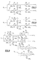
- lines 11 and 12 include each two reversing doors in cascade, respectively 20, 21 and 22, 23, and are strictly identical.
- Door 20 is strictly identical, within the limits of manufacturing technology, to the door 22, and door 21 strictly identical to the door 23.
- the output of door 20 is connected to a terminal of a buffer capacity 24 of which the other terminal is connected to ground.
- This capacity 24 is added to the parasitic output capacity of door 20 and allows calibrate the time constant T of line 11.
- a buffer capacity 25 strictly identical to the capacity 24.
- Doors 20 to 23 are supplied with voltage Vcc taken from the same point PV1 of a plane and are connected to the same point of GND1 mass of a ground plane.
- the ground terminal of the capacity 24 is connected to GND1 earth point then that the ground terminal of capacity 25 is connected to another GND2 ground point, taken from another location of the ground plan.
- electronic noise differential N1 is injected into the earth terminal of the capacity 25.
- the noise N1 here is equal to the difference of voltage between GND2 and GND1 ground points, and causes a random imbalance in the constants of time of the two delay lines 11, 12.
- Pulsed signals S1, S2 at the end of lines 11, 12 are offset randomly, as illustrated in Figure 6.
- FIG 8 Another example of noise injection is illustrated in figure 8.
- all the elements are connected to GND1 ground point except for the door 23 of line 12, which has its earth terminal connected to GND2 ground point.
- Differential noise N1 is. so injected here on the mass of door 23, and randomly modifies the threshold voltage VTN23 by low switching (change to 0) of this door.
- the random modification of the threshold voltage VTN23 se translated by a random imbalance of the constant of time on line 12.
- all logic gates have their power supply terminal connected to point PV1 of the feeding plan, with the exception of door 20 which has its power supply terminal connected to another point PV2 supply, taken from another location on the plan Power.
- a differential noise N2 is therefore injected on the power supply of door 20 and modify randomly its switching threshold voltage VTP20 high (change to 1), which causes an imbalance additional time between lines 11 and 12.
- N1 and N2 noise injections which have just been described. So the ground bounds of gate 23 and capacity 25 receive noise N1 and the power terminal of door 20 receives noise N2.
- a capacity 26 is added in parallel with capacity 24 from line 11 and capacity 27 is added in parallel with capacity 25 of line 12.
- Capacities 26 and 27 are identical but receive on their earth terminal oscillating signals H1, H2 delivered by different OSC1, OSC2 oscillators having different natural frequencies. So the H1 signal injects into line 11 an additional noise N3 and the signal H2 injects noise into line 12 additional N4.
- the resulting differential noise is a non-random cyclic noise which, however, fairly long cycle time (multiple of frequencies of the two oscillators OSC1, OSC2).
- the delay lines according to the invention can be the subject of various other variants of realization and improvements.
- the delay lines 11, 12 shown on the Figures 7 to 9 have only two reversing doors cascading for the sake of simplicity of description, it is obvious that this number can be increased and chosen according to the time constant that one wish to obtain and switching characteristics logic gates.
- multiple points noise injection can be provided.
- CMOS doors allows you to control the consumption of the generator 10 according to the invention.
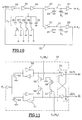
- doors 20 and 22 whose exits attack capacities 24, 26 and 25, 27 can be supplied via current generators 28, 29 to low flow, as illustrated in figure 9 (you can also size the size of the transistor drain PMOS which it comprises so as to limit the current of Switching).
- CMOS doors only consume current when switching, PMOS transistors 30, 31 mounted in accelerators switching can be provided between the outputs of the doors 21 and 23 and their entrances, as illustrated in figure 9.
- one of the delay lines here line 12 has its output brought back to its input by means of inverting doors 32, 33, 34 in cascade.
- the assembly forms an oscillator loop OL making it possible to generate in situ the reference signal Hr applied to the input of lines 11, 12.
- the output of line 12 is brought back to input via of a NAND gate 32 controlled by an activation signal ACTIV of the generator, and of two reversing doors 33, 34.
- the total number of reversing doors of the oscillator loop OL must be, in a conventional manner, odd.
- the output of a reversing door of the OL loop has at its output a variable buffer capacity Cv.
- Cv capacity includes in parallel a capacity 35 and capacities 36 39 switchable by MOS transistors controlled by signals A, B, C, D. These signals can be taken at any point on an integrated circuit, for example in a address or data bus, or at the exit of the generator 10.
- the modification of the Cv capacity causes a change in the resonant frequency of the OL oscillator loop.
- FIG. 11 represents an embodiment of the circuit 13 in FIG. 5.
- Circuit 13 comprises two memory inverters 50, 51 whose inputs are connected to ground through two transistors 52, 53, respectively.
- the signal from reference Hr controls the transistors 52, 53 by through a reversing door.
- the outputs of inverters 50, 51 respectively attack input S and the input C of a flip-flop 54 of type S-C.
- the Q output of flip-flop 54 delivers the RS signal and the / Q output delivers the reverse signal / RS.
- the output of the inverter 50 is connected to ground via two transistors 55, 56 in series.
- the transistor 55 is controlled by the signal S1 and the transistor 56 is controlled by the output of the inverter 51.
- Symmetrically, the output of the inverter 51 is connected to ground by through two transistors 57, 58.
- the transistor 57 is driven by signal S2 and transistor 58 is controlled by the output of the inverter 50.
- the present invention is susceptible to various variations of realization and improvements.
- various methods exist in practice for obtaining perfectly symmetrical delay lines in the absence of electronic noise. These methods are know-how skilled in the art and have not been described in a concern for simplicity.
- forecasting several pairs of delay lines in parallel each having their own oscillator loop or a common oscillator loop, provides in a stroke of the clock a random word comprising a plurality of bits in parallel.
- the delay lines according to the invention have been presented as consisting of logic gates, it is quite obvious that these delay lines can be performed in various other known ways.
- the random generator according to the invention because of its simplicity and its low current consumption, particularly suitable integrated circuits of smart cards, especially integrated circuits of contactless smart cards powered by electromagnetic induction and having low energy resources.
Landscapes
- Physics & Mathematics (AREA)
- Theoretical Computer Science (AREA)
- General Physics & Mathematics (AREA)
- Engineering & Computer Science (AREA)
- Mathematical Optimization (AREA)
- Pure & Applied Mathematics (AREA)
- Mathematical Analysis (AREA)
- General Engineering & Computer Science (AREA)
- Computational Mathematics (AREA)
- Manipulation Of Pulses (AREA)
- Polarising Elements (AREA)
- Crystals, And After-Treatments Of Crystals (AREA)
- Preparation Of Compounds By Using Micro-Organisms (AREA)
- Analogue/Digital Conversion (AREA)
- Transition And Organic Metals Composition Catalysts For Addition Polymerization (AREA)
- Details Of Television Scanning (AREA)
Description
- la figure 1 précédemment décrite est le schéma électronique d'un générateur aléatoire classique,
- la figure 2 précédemment décrite représente des signaux présents dans le générateur de la figure 1,
- les figures 3 et 4 précédemment décrites représentent un bruit électronique et une tension de référence appliqués au générateur de la figure 1,
- la figure 5 représente sous forme de blocs un générateur aléatoire selon l'invention,
- la figure 6 représente divers signaux apparaissant dans le générateur de la figure 5,
- les figures 7 à 10 représentent des exemples de réalisation de lignes à retard selon l'invention, représentées sous forme de blocs en figure 5, et.
- la figure 11 est le schéma électrique d'un élément du générateur de la figure 5.
- "11" : réception d'une impulsion à 0 du signal Hr (phase d'initialisation),
- "01" : réception d'une impulsion S1 avant une impulsion S2, ou
- "10" : réception d'un impulsion S2 avant une impulsion S1,
Claims (10)
- Générateur (10) de signal aléatoire agencé pour transformer un bruit électronique (N, N1, N2) en un signal logique (RS) dont la valeur dépend des fluctuations aléatoires du bruit électronique (N, N1, N2), caractérisé en ce qu'il comprend :des moyens (11, 12) pour transformer au moins un bruit électronique (N, N1, N2) en un décalage temporel d'au moins deux signaux pulsés (S1, S2) issus d'un même signal pulsé de référence (Hr), etdes moyens (13) pour délivrer un signal logique (RS) dont la valeur est fonction du décalage temporel relatif (+Δt, -Δt) des deux signaux pulsés (S1, S2).
- Générateur (10) selon la revendication 1, dans lequel les moyens pour transformer au moins un bruit électronique comprennent :au moins deux lignes à retard (11, 12) ayant des constantes de temps (T) initialement équilibrées, recevant en entrée ledit signal pulsé de référence (Hr),des moyens (20, 22, 23, 25) pour injecter au moins un bruit électronique (N, N1, N2) dans au moins l'une des lignes à retard (11, 12), de manière à faire fluctuer sa constante de temps (T).
- Générateur selon la revendication 2, dans lequel :les lignes à retard (11, 12) comprennent des portes logiques (20-23) en cascade, etau moins une porte logique (20, 22, 23) d'au moins une ligne à retard (11, 12) reçoit au moins un bruit électronique (N1, N2) faisant fluctuer sa constante de temps de commutation.
- Générateur selon la revendication 3, dans lequel le bruit électronique (N1, N2) est appliqué sur la borne de masse ou la borne d'alimentation de la porte logique (20, 23).
- Générateur selon l'une des revendications 3 et 4, dans lequel le bruit électronique (N1) est appliqué sur la borne de masse d'une capacité tampon (25) connectée à la sortie de la porte logique (22).
- Générateur selon l'une des revendications précédentes, caractérisé en ce que le bruit électronique (N1, N2) est un bruit différentiel prélevé en deux points (GND1, GND2) d'un plan de masse.
- Générateur selon l'une des revendications précédentes, caractérisé en ce que le bruit électronique (N1, N2) est un bruit différentiel prélevé en deux points (PV1, PV2) d'un plan d'alimentation électrique.
- Générateur selon l'une des revendications 2 à 7, caractérisé en ce qu'il comprend au moins deux oscillateurs distincts (OSC1, OSC2) pour délivrer deux signaux oscillants (H1, H2) non corrélés, et en ce que lesdits signaux oscillants sont injectés en tant que bruit complémentaire (N3, N4) dans les lignes à retard.
- Générateur selon l'une des revendications 2 à 8, dans lequel la sortie de l'une des lignes à retard (12) est ramenée sur son entrée par l'intermédiaire de portes logiques (32, 33, 34) pour former un oscillateur délivrant ledit signal pulsé de référence (Hr).
- Générateur (1) selon l'une des revendications précédentes, comprenant des moyens pour échantillonner le signal logique (RS) au rythme d'un signal de synchronisation (Hs).
Applications Claiming Priority (3)
| Application Number | Priority Date | Filing Date | Title |
|---|---|---|---|
| FR9711210 | 1997-09-10 | ||
| FR9711210A FR2768276B1 (fr) | 1997-09-10 | 1997-09-10 | Generateur d'alea |
| PCT/FR1998/001907 WO1999013572A1 (fr) | 1997-09-10 | 1998-09-07 | Generateur d'alea |
Publications (2)
| Publication Number | Publication Date |
|---|---|
| EP1012972A1 EP1012972A1 (fr) | 2000-06-28 |
| EP1012972B1 true EP1012972B1 (fr) | 2002-01-23 |
Family
ID=9510910
Family Applications (1)
| Application Number | Title | Priority Date | Filing Date |
|---|---|---|---|
| EP98942833A Expired - Lifetime EP1012972B1 (fr) | 1997-09-10 | 1998-09-07 | Generateur d'alea |
Country Status (8)
| Country | Link |
|---|---|
| US (1) | US6247033B1 (fr) |
| EP (1) | EP1012972B1 (fr) |
| CN (1) | CN1134891C (fr) |
| AT (1) | ATE212485T1 (fr) |
| AU (1) | AU9081498A (fr) |
| DE (1) | DE69803584T2 (fr) |
| FR (1) | FR2768276B1 (fr) |
| WO (1) | WO1999013572A1 (fr) |
Cited By (1)
| Publication number | Priority date | Publication date | Assignee | Title |
|---|---|---|---|---|
| WO2012149944A1 (fr) | 2011-05-03 | 2012-11-08 | Novomatic Ag | Générateur de nombres aléatoires |
Families Citing this family (17)
| Publication number | Priority date | Publication date | Assignee | Title |
|---|---|---|---|---|
| FR2783374B1 (fr) * | 1998-09-11 | 2000-12-08 | Thomson Csf | Procede et dispositif de generation d'un signal aleatoire et systemes de conversion numerique-analogique utilisant un tel signal aleatoire |
| US7243117B2 (en) * | 2001-02-07 | 2007-07-10 | Fdk Corporation | Random number generator and probability generator |
| DE10117362A1 (de) * | 2001-04-06 | 2002-10-17 | Infineon Technologies Ag | Zufallszahlengenerator und Verfahren zum Erzeugen einer Zufallszahl |
| RU2191421C1 (ru) * | 2001-08-08 | 2002-10-20 | Федеральное Государственное Унитарное Предприятие "Концерн "Системпром" | Генератор последовательности случайных чисел |
| US7188131B2 (en) * | 2002-11-27 | 2007-03-06 | Stmicroelectronics S.A. | Random number generator |
| EP1562291B1 (fr) * | 2004-02-04 | 2007-04-18 | Infineon Technologies AG | Dispositif de production d'une séquence binaire aléatoire |
| US8407097B2 (en) * | 2004-04-15 | 2013-03-26 | Hand Held Products, Inc. | Proximity transaction apparatus and methods of use thereof |
| EP1887459B1 (fr) * | 2004-10-15 | 2010-09-29 | Nxp B.V. | Circuit intégré à générateur de vrais nombres aléatoires |
| DE602005008362D1 (de) * | 2005-01-28 | 2008-09-04 | Infineon Technologies Ag | Oszillator-basierter Zufallszahlengenerator |
| DE102005009190B3 (de) * | 2005-03-01 | 2006-05-18 | Matthias Braeunig | Verfahren und Anordnung zur Erzeugung einer Daten-Bitfolge durch Abtasten eines digitalisierten Rauschsignals |
| EP1763136A1 (fr) * | 2005-09-07 | 2007-03-14 | Stmicroelectronics Sa | Procédé de génération de nombres variables |
| US20070109103A1 (en) * | 2005-09-07 | 2007-05-17 | California Institute Of Technology | Commercial product activation and monitoring using radio frequency identification (RFID) technology |
| US20090223738A1 (en) * | 2008-02-22 | 2009-09-10 | Yamaha Corporation | Sound absorbing structure and vehicle component having sound absorption property |
| FR3072481B1 (fr) * | 2017-10-12 | 2019-11-08 | Stmicroelectronics | Dispositif de generation d'un signal aleatoire |
| CN112005496A (zh) * | 2019-03-26 | 2020-11-27 | 深圳市汇顶科技股份有限公司 | 具有随机信号发生器件的集成装置、制备方法及电子设备 |
| CN114204920B (zh) * | 2020-09-02 | 2023-04-07 | 圣邦微电子(北京)股份有限公司 | 信号处理电路 |
| JP2024108600A (ja) * | 2023-01-31 | 2024-08-13 | シャープセミコンダクターイノベーション株式会社 | 電子回路 |
Family Cites Families (7)
| Publication number | Priority date | Publication date | Assignee | Title |
|---|---|---|---|---|
| US4183088A (en) * | 1962-01-31 | 1980-01-08 | The United States Of America As Represented By The Secretary Of The Navy | Random number generator |
| US3612845A (en) * | 1968-07-05 | 1971-10-12 | Reed C Lawlor | Computer utilizing random pulse trains |
| FR2390047B1 (fr) * | 1977-05-06 | 1982-09-17 | Aerospatiale | |
| US4513386A (en) * | 1982-11-18 | 1985-04-23 | Ncr Corporation | Random binary bit signal generator |
| SU1157671A1 (ru) * | 1983-07-13 | 1985-05-23 | Казанский Ордена Трудового Красного Знамени И Ордена Дружбы Народов Авиационный Институт Им.А.Н.Туполева | Устройство задержки импульсов |
| JP2577999B2 (ja) * | 1989-09-28 | 1997-02-05 | クラリオン株式会社 | 擬似雑音符号発生装置における先頭又は任意ビットパルス生成回路およびサンプリングパルス生成回路 |
| US5627775A (en) * | 1995-04-18 | 1997-05-06 | Applied Computing Systems, Inc. | Method and apparatus for generating random numbers using electrical noise |
-
1997
- 1997-09-10 FR FR9711210A patent/FR2768276B1/fr not_active Expired - Fee Related
-
1998
- 1998-09-07 WO PCT/FR1998/001907 patent/WO1999013572A1/fr not_active Ceased
- 1998-09-07 DE DE69803584T patent/DE69803584T2/de not_active Expired - Lifetime
- 1998-09-07 AT AT98942833T patent/ATE212485T1/de active
- 1998-09-07 EP EP98942833A patent/EP1012972B1/fr not_active Expired - Lifetime
- 1998-09-07 CN CNB98811013XA patent/CN1134891C/zh not_active Expired - Lifetime
- 1998-09-07 AU AU90814/98A patent/AU9081498A/en not_active Abandoned
-
2000
- 2000-03-10 US US09/523,270 patent/US6247033B1/en not_active Expired - Lifetime
Cited By (1)
| Publication number | Priority date | Publication date | Assignee | Title |
|---|---|---|---|---|
| WO2012149944A1 (fr) | 2011-05-03 | 2012-11-08 | Novomatic Ag | Générateur de nombres aléatoires |
Also Published As
| Publication number | Publication date |
|---|---|
| US6247033B1 (en) | 2001-06-12 |
| EP1012972A1 (fr) | 2000-06-28 |
| DE69803584D1 (de) | 2002-03-14 |
| AU9081498A (en) | 1999-03-29 |
| CN1278965A (zh) | 2001-01-03 |
| FR2768276B1 (fr) | 2000-06-02 |
| ATE212485T1 (de) | 2002-02-15 |
| CN1134891C (zh) | 2004-01-14 |
| FR2768276A1 (fr) | 1999-03-12 |
| DE69803584T2 (de) | 2002-10-02 |
| WO1999013572A1 (fr) | 1999-03-18 |
Similar Documents
| Publication | Publication Date | Title |
|---|---|---|
| EP1012972A1 (fr) | Generateur d'alea | |
| US8285767B2 (en) | Apparatus and method for generating a random number | |
| EP3242398B1 (fr) | Générateur de nombres d'oscillations | |
| EP1204948B1 (fr) | Micro-controleur securise contre les attaques en courant | |
| EP0898356B1 (fr) | Pompes de charge à fréquence variable | |
| FR2707059A1 (fr) | ||
| EP0442829B1 (fr) | Doubleur de fréquence d'horloge | |
| EP3242401A1 (fr) | Circuit de comptage d'impulsions | |
| EP1107503B1 (fr) | Composant électronique de sécurité | |
| EP3376670B1 (fr) | Ligne à retard configurable | |
| EP1606880B1 (fr) | Diviseur de frequence a taux de division variable | |
| FR2785068A1 (fr) | Procede et dispositif de codage pour la transmission de donnees par modulation de charge et couplage inductif | |
| FR2817361A1 (fr) | Generateur de signal aleatoire | |
| CN101989857B (zh) | 用于在半导体集成电路中产生时钟的装置 | |
| EP0678868B1 (fr) | Circuit multiplicateur de tension | |
| FR2532777A1 (fr) | Circuit de translation de signaux | |
| EP1120714B1 (fr) | Dispositif de régénération d'une horloge | |
| FR2604577A1 (fr) | Circuit generateur de code a bruit pseudo-aleatoire | |
| WO2007080242A1 (fr) | Diviseur de frequence binaire | |
| FR2573561A1 (fr) | Element de memoire dynamique, bascule maitre-esclave et circuits sequentiels programmables utilisant cet element de memoire dynamique | |
| TWI239144B (en) | Digitized deskew buffer and its operation method of communication transmission machine | |
| EP1763136A1 (fr) | Procédé de génération de nombres variables | |
| FR2664421A1 (fr) | Decodeur precharge a autoverrouillage. | |
| FR2476893A1 (fr) | Registre a decalage statique i2l | |
| JPH09130213A (ja) | ダイナミックラッチ回路 |
Legal Events
| Date | Code | Title | Description |
|---|---|---|---|
| PUAI | Public reference made under article 153(3) epc to a published international application that has entered the european phase |
Free format text: ORIGINAL CODE: 0009012 |
|
| 17P | Request for examination filed |
Effective date: 20000226 |
|
| AK | Designated contracting states |
Kind code of ref document: A1 Designated state(s): AT BE CH CY DE DK ES FI FR GB GR IE IT LI LU MC NL PT SE |
|
| GRAG | Despatch of communication of intention to grant |
Free format text: ORIGINAL CODE: EPIDOS AGRA |
|
| 17Q | First examination report despatched |
Effective date: 20010321 |
|
| GRAG | Despatch of communication of intention to grant |
Free format text: ORIGINAL CODE: EPIDOS AGRA |
|
| GRAH | Despatch of communication of intention to grant a patent |
Free format text: ORIGINAL CODE: EPIDOS IGRA |
|
| GRAH | Despatch of communication of intention to grant a patent |
Free format text: ORIGINAL CODE: EPIDOS IGRA |
|
| GRAA | (expected) grant |
Free format text: ORIGINAL CODE: 0009210 |
|
| REG | Reference to a national code |
Ref country code: GB Ref legal event code: IF02 |
|
| AK | Designated contracting states |
Kind code of ref document: B1 Designated state(s): AT BE CH CY DE DK ES FI FR GB GR IE IT LI LU MC NL PT SE |
|
| PG25 | Lapsed in a contracting state [announced via postgrant information from national office to epo] |
Ref country code: NL Free format text: LAPSE BECAUSE OF FAILURE TO SUBMIT A TRANSLATION OF THE DESCRIPTION OR TO PAY THE FEE WITHIN THE PRESCRIBED TIME-LIMIT Effective date: 20020123 Ref country code: IT Free format text: LAPSE BECAUSE OF FAILURE TO SUBMIT A TRANSLATION OF THE DESCRIPTION OR TO PAY THE FEE WITHIN THE PRESCRIBED TIME-LIMIT;WARNING: LAPSES OF ITALIAN PATENTS WITH EFFECTIVE DATE BEFORE 2007 MAY HAVE OCCURRED AT ANY TIME BEFORE 2007. THE CORRECT EFFECTIVE DATE MAY BE DIFFERENT FROM THE ONE RECORDED. Effective date: 20020123 Ref country code: IE Free format text: LAPSE BECAUSE OF FAILURE TO SUBMIT A TRANSLATION OF THE DESCRIPTION OR TO PAY THE FEE WITHIN THE PRESCRIBED TIME-LIMIT Effective date: 20020123 Ref country code: GR Free format text: LAPSE BECAUSE OF FAILURE TO SUBMIT A TRANSLATION OF THE DESCRIPTION OR TO PAY THE FEE WITHIN THE PRESCRIBED TIME-LIMIT Effective date: 20020123 Ref country code: FI Free format text: LAPSE BECAUSE OF FAILURE TO SUBMIT A TRANSLATION OF THE DESCRIPTION OR TO PAY THE FEE WITHIN THE PRESCRIBED TIME-LIMIT Effective date: 20020123 Ref country code: AT Free format text: LAPSE BECAUSE OF FAILURE TO SUBMIT A TRANSLATION OF THE DESCRIPTION OR TO PAY THE FEE WITHIN THE PRESCRIBED TIME-LIMIT Effective date: 20020123 |
|
| REF | Corresponds to: |
Ref document number: 212485 Country of ref document: AT Date of ref document: 20020215 Kind code of ref document: T |
|
| REG | Reference to a national code |
Ref country code: CH Ref legal event code: EP |
|
| REG | Reference to a national code |
Ref country code: IE Ref legal event code: FG4D Free format text: FRENCH |
|
| REF | Corresponds to: |
Ref document number: 69803584 Country of ref document: DE Date of ref document: 20020314 |
|
| PG25 | Lapsed in a contracting state [announced via postgrant information from national office to epo] |
Ref country code: SE Free format text: LAPSE BECAUSE OF FAILURE TO SUBMIT A TRANSLATION OF THE DESCRIPTION OR TO PAY THE FEE WITHIN THE PRESCRIBED TIME-LIMIT Effective date: 20020423 Ref country code: PT Free format text: LAPSE BECAUSE OF FAILURE TO SUBMIT A TRANSLATION OF THE DESCRIPTION OR TO PAY THE FEE WITHIN THE PRESCRIBED TIME-LIMIT Effective date: 20020423 Ref country code: DK Free format text: LAPSE BECAUSE OF FAILURE TO SUBMIT A TRANSLATION OF THE DESCRIPTION OR TO PAY THE FEE WITHIN THE PRESCRIBED TIME-LIMIT Effective date: 20020423 |
|
| GBT | Gb: translation of ep patent filed (gb section 77(6)(a)/1977) |
Effective date: 20020419 |
|
| NLV1 | Nl: lapsed or annulled due to failure to fulfill the requirements of art. 29p and 29m of the patents act | ||
| PG25 | Lapsed in a contracting state [announced via postgrant information from national office to epo] |
Ref country code: ES Free format text: LAPSE BECAUSE OF FAILURE TO SUBMIT A TRANSLATION OF THE DESCRIPTION OR TO PAY THE FEE WITHIN THE PRESCRIBED TIME-LIMIT Effective date: 20020730 |
|
| REG | Reference to a national code |
Ref country code: IE Ref legal event code: FD4D |
|
| PG25 | Lapsed in a contracting state [announced via postgrant information from national office to epo] |
Ref country code: LU Free format text: LAPSE BECAUSE OF NON-PAYMENT OF DUE FEES Effective date: 20020907 |
|
| PG25 | Lapsed in a contracting state [announced via postgrant information from national office to epo] |
Ref country code: CY Free format text: LAPSE BECAUSE OF FAILURE TO SUBMIT A TRANSLATION OF THE DESCRIPTION OR TO PAY THE FEE WITHIN THE PRESCRIBED TIME-LIMIT Effective date: 20020930 Ref country code: BE Free format text: LAPSE BECAUSE OF NON-PAYMENT OF DUE FEES Effective date: 20020930 |
|
| PLBE | No opposition filed within time limit |
Free format text: ORIGINAL CODE: 0009261 |
|
| STAA | Information on the status of an ep patent application or granted ep patent |
Free format text: STATUS: NO OPPOSITION FILED WITHIN TIME LIMIT |
|
| 26N | No opposition filed | ||
| BERE | Be: lapsed |
Owner name: *INSIDE TECHNOLOGIES Effective date: 20020930 |
|
| PG25 | Lapsed in a contracting state [announced via postgrant information from national office to epo] |
Ref country code: MC Free format text: LAPSE BECAUSE OF NON-PAYMENT OF DUE FEES Effective date: 20030401 |
|
| REG | Reference to a national code |
Ref country code: FR Ref legal event code: CD Ref country code: FR Ref legal event code: CA |
|
| REG | Reference to a national code |
Ref country code: CH Ref legal event code: PFA Owner name: INSIDE CONTACTLESS Free format text: INSIDE TECHNOLOGIES#PEPINIERE AXONE#69930 SAINT-CLEMENT-LES-PLACES (FR) -TRANSFER TO- INSIDE CONTACTLESS#BAT. 11 A - PARC CLUB DU GOLF#13856 AIX-EN-PROVENCE CEDEX 3 (FR) |
|
| PGFP | Annual fee paid to national office [announced via postgrant information from national office to epo] |
Ref country code: CH Payment date: 20090825 Year of fee payment: 12 |
|
| REG | Reference to a national code |
Ref country code: CH Ref legal event code: PL |
|
| PG25 | Lapsed in a contracting state [announced via postgrant information from national office to epo] |
Ref country code: LI Free format text: LAPSE BECAUSE OF NON-PAYMENT OF DUE FEES Effective date: 20100930 Ref country code: CH Free format text: LAPSE BECAUSE OF NON-PAYMENT OF DUE FEES Effective date: 20100930 |
|
| REG | Reference to a national code |
Ref country code: DE Ref legal event code: R082 Ref document number: 69803584 Country of ref document: DE Representative=s name: HOFFMANN - EITLE, DE |
|
| REG | Reference to a national code |
Ref country code: DE Ref legal event code: R082 Ref document number: 69803584 Country of ref document: DE Representative=s name: HOFFMANN - EITLE PATENT- UND RECHTSANWAELTE PA, DE Effective date: 20131111 Ref country code: DE Ref legal event code: R082 Ref document number: 69803584 Country of ref document: DE Representative=s name: HOFFMANN - EITLE, DE Effective date: 20131111 Ref country code: DE Ref legal event code: R081 Ref document number: 69803584 Country of ref document: DE Owner name: INSIDE SECURE, FR Free format text: FORMER OWNER: INSIDE TECHNOLOGIES, SAINT-CLEMENT-LES-PLACES, FR Effective date: 20131111 |
|
| REG | Reference to a national code |
Ref country code: FR Ref legal event code: CD Owner name: INSIDE SECURE Effective date: 20140129 Ref country code: FR Ref legal event code: CA Effective date: 20140129 |
|
| REG | Reference to a national code |
Ref country code: FR Ref legal event code: PLFP Year of fee payment: 19 |
|
| REG | Reference to a national code |
Ref country code: FR Ref legal event code: PLFP Year of fee payment: 20 |
|
| PGFP | Annual fee paid to national office [announced via postgrant information from national office to epo] |
Ref country code: GB Payment date: 20170821 Year of fee payment: 20 Ref country code: FR Payment date: 20170919 Year of fee payment: 20 Ref country code: DE Payment date: 20170821 Year of fee payment: 20 |
|
| REG | Reference to a national code |
Ref country code: DE Ref legal event code: R071 Ref document number: 69803584 Country of ref document: DE |
|
| REG | Reference to a national code |
Ref country code: GB Ref legal event code: PE20 Expiry date: 20180906 |
|
| PG25 | Lapsed in a contracting state [announced via postgrant information from national office to epo] |
Ref country code: GB Free format text: LAPSE BECAUSE OF EXPIRATION OF PROTECTION Effective date: 20180906 |