EP1204948B1 - Micro-controleur securise contre les attaques en courant - Google Patents
Micro-controleur securise contre les attaques en courant Download PDFInfo
- Publication number
- EP1204948B1 EP1204948B1 EP00953248A EP00953248A EP1204948B1 EP 1204948 B1 EP1204948 B1 EP 1204948B1 EP 00953248 A EP00953248 A EP 00953248A EP 00953248 A EP00953248 A EP 00953248A EP 1204948 B1 EP1204948 B1 EP 1204948B1
- Authority
- EP
- European Patent Office
- Prior art keywords
- microcontroller
- μce
- cap
- com
- efficient
- Prior art date
- Legal status (The legal status is an assumption and is not a legal conclusion. Google has not performed a legal analysis and makes no representation as to the accuracy of the status listed.)
- Expired - Lifetime
Links
Images


Classifications
-
- H—ELECTRICITY
- H01—ELECTRIC ELEMENTS
- H01L—SEMICONDUCTOR DEVICES NOT COVERED BY CLASS H10
- H01L23/00—Details of semiconductor or other solid state devices
- H01L23/57—Protection from inspection, reverse engineering or tampering
- H01L23/576—Protection from inspection, reverse engineering or tampering using active circuits
-
- G—PHYSICS
- G06—COMPUTING; CALCULATING OR COUNTING
- G06K—GRAPHICAL DATA READING; PRESENTATION OF DATA; RECORD CARRIERS; HANDLING RECORD CARRIERS
- G06K19/00—Record carriers for use with machines and with at least a part designed to carry digital markings
- G06K19/06—Record carriers for use with machines and with at least a part designed to carry digital markings characterised by the kind of the digital marking, e.g. shape, nature, code
- G06K19/067—Record carriers with conductive marks, printed circuits or semiconductor circuit elements, e.g. credit or identity cards also with resonating or responding marks without active components
- G06K19/07—Record carriers with conductive marks, printed circuits or semiconductor circuit elements, e.g. credit or identity cards also with resonating or responding marks without active components with integrated circuit chips
- G06K19/073—Special arrangements for circuits, e.g. for protecting identification code in memory
- G06K19/07309—Means for preventing undesired reading or writing from or onto record carriers
- G06K19/07363—Means for preventing undesired reading or writing from or onto record carriers by preventing analysis of the circuit, e.g. dynamic or static power analysis or current analysis
-
- H—ELECTRICITY
- H01—ELECTRIC ELEMENTS
- H01L—SEMICONDUCTOR DEVICES NOT COVERED BY CLASS H10
- H01L2224/00—Indexing scheme for arrangements for connecting or disconnecting semiconductor or solid-state bodies and methods related thereto as covered by H01L24/00
- H01L2224/01—Means for bonding being attached to, or being formed on, the surface to be connected, e.g. chip-to-package, die-attach, "first-level" interconnects; Manufacturing methods related thereto
- H01L2224/42—Wire connectors; Manufacturing methods related thereto
- H01L2224/47—Structure, shape, material or disposition of the wire connectors after the connecting process
- H01L2224/48—Structure, shape, material or disposition of the wire connectors after the connecting process of an individual wire connector
- H01L2224/4805—Shape
- H01L2224/4809—Loop shape
- H01L2224/48091—Arched
-
- H—ELECTRICITY
- H01—ELECTRIC ELEMENTS
- H01L—SEMICONDUCTOR DEVICES NOT COVERED BY CLASS H10
- H01L2224/00—Indexing scheme for arrangements for connecting or disconnecting semiconductor or solid-state bodies and methods related thereto as covered by H01L24/00
- H01L2224/01—Means for bonding being attached to, or being formed on, the surface to be connected, e.g. chip-to-package, die-attach, "first-level" interconnects; Manufacturing methods related thereto
- H01L2224/42—Wire connectors; Manufacturing methods related thereto
- H01L2224/47—Structure, shape, material or disposition of the wire connectors after the connecting process
- H01L2224/48—Structure, shape, material or disposition of the wire connectors after the connecting process of an individual wire connector
- H01L2224/481—Disposition
- H01L2224/48151—Connecting between a semiconductor or solid-state body and an item not being a semiconductor or solid-state body, e.g. chip-to-substrate, chip-to-passive
- H01L2224/48221—Connecting between a semiconductor or solid-state body and an item not being a semiconductor or solid-state body, e.g. chip-to-substrate, chip-to-passive the body and the item being stacked
- H01L2224/48225—Connecting between a semiconductor or solid-state body and an item not being a semiconductor or solid-state body, e.g. chip-to-substrate, chip-to-passive the body and the item being stacked the item being non-metallic, e.g. insulating substrate with or without metallisation
- H01L2224/48227—Connecting between a semiconductor or solid-state body and an item not being a semiconductor or solid-state body, e.g. chip-to-substrate, chip-to-passive the body and the item being stacked the item being non-metallic, e.g. insulating substrate with or without metallisation connecting the wire to a bond pad of the item
- H01L2224/48228—Connecting between a semiconductor or solid-state body and an item not being a semiconductor or solid-state body, e.g. chip-to-substrate, chip-to-passive the body and the item being stacked the item being non-metallic, e.g. insulating substrate with or without metallisation connecting the wire to a bond pad of the item the bond pad being disposed in a recess of the surface of the item
Definitions
- the invention relates to microcontrollers intended to be embedded in portable objects and, in particular, in such map-sized objects more commonly referred to as smart cards.
- Smart cards are generally used in applications in which security of storage and data processing confidential are essential. They are intended in particular for applications in the field of health, to television applications toll, or even banking applications for example electronic purse.
- Micro-controllers are programmed automatic controllers in the form of an integrated circuit. They apply a sequence of instructions logical data to data from their internal memories or from from the outside world, via an input / output pad.
- micro-smart card controllers are designed in CMOS technology. This technology makes it possible to integrate same circuit, subsets useful for the operation of the microcontroller, that is to say in particular a central processing unit CPU, non-volatile non-rewritable memories and read-only ROM (Read Only Memory), non-volatile memory Rewritable type Flash.
- EEPROM Electrically Erasable Programmable Read Only Memory
- FRAM Feromagnetic Random Access Memory
- volatile memory RAM Random Access Memory
- Fraudsters have developed so-called current attacks in order to to obtain confidential data managed by the micro-controller and for example keys intended for the implementation of algorithms of encryption implemented in micro-controllers such as algorithms known as DES (Data Encryption Standard) or RSA (Rivest Shamir Adelman).
- DES Data Encryption Standard
- RSA Raster Shamir Adelman
- the fraudsters connect in particular a resistor R of low value, in particular of 1 ⁇ , in series between a voltage supply source V ⁇ C of the microcontroller and its power supply pad VCC . They then display the variations of the voltage R Icc (t) as a function of time obtained in response to the execution of several hundreds or even thousands of instructions applied to identical, similar or different operands by means of a coupled computer. for example, to a digital oscilloscope that amplifies these variations, they sample and digitize the results obtained for a non-real-time analysis.
- US Pat. No. 4,932,053 relates to security confidential information contained in an integrated circuit.
- a circuit of protection is used. This protection circuit makes it possible to activate the simulation, according to a pseudo-random sequence generated by a generators, current consumption values identical to those real memory cells.
- US Pat. No. 4,827,451 relates to the field of memories constructed as a matrix of memory cells. Said cells, being accessible by the rows and columns, are connected to read and write circuits that are used to program them according to two states - "1" or "0" according to the data of inputs - and read the state thus programmed.
- the memory cells are type requiring a programming current in order to be programmed at "1” and does not require any current when programming at "0".
- Said security circuit consists of a simulation circuit activating when programming to "0" to deliver a current identical to the one delivered by a memory cell during a "1" programming.
- a technical problem proposes to solve the invention is to secure a portable object of the type smart card.
- the present invention is as defined in the reventications whose preambles are constituted by the characteristics described in US 4,932,053 and US 4,827,451.
- the means for varying the supply voltage of the effective data processing part comprise: a variable resistance as a function of time connected in series with the supply pad of the microcontroller, this variable resistor being for example an open switch during time intervals T off and closed during time intervals T on , the duty cycle T off / (T on + T off ) varying as a function of time, the period T on + T off varying in function of time.
- the means for varying the supply voltage of the effective part of data processing include advantageously a pulse generator, this generator of pulses comprising a synchronization circuit of crossing of voltage threshold across the effective part of data processing.
- the means for varying the supply voltage of the effective part of data processing furthermore comprise advantageously a capacitor, this capacitor being for example a capacity with a capacity greater than 0.1 nanofarad.
- the microcontroller comprises a main layer of silicon whose active face, which incorporates a circuit and carries the contact pads, is sealed to a complementary layer of protection by means of a sealing layer, the means for varying the tension feeding of the effective part of data processing being located in the complementary protective layer.
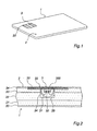
- an object portable device is in the form of a card 1 substantially parallelepipedal rectangular and thin one of which body 2 incorporates an electronic module 3.
- the card body 2 consists of five sheets 20, 21, 22, 23 and 24 laminated plastics and has a cavity 25 for the incorporation of module 3.
- the module 3 comprises a microcontroller 30 whose pads 300 electrically connected by means of wires 31 conductors, to flush contact pads 32 on the surface of the card body 2. These beaches 32 are based on a thickness 33 of a dielectric epoxy glass type.
- the microcontroller assembly 30 and wires 31 conductors is embedded in a protective resin 34.
- the microcontroller 30 is in the form of a rectangular parallelepiped whose thickness is of the order of 180 ⁇ m and whose surface is of the order of 10 mm 2 .
- This microcontroller 30 comprises a main layer 301 of silicon whose active face, which integrates a circuit and carries the studs 300 contact is sealed to a complementary layer 302 of protection of silicon by means of a sealing layer 303.
- This layer complementary 302 is provided with openings 304 located in line with pads 300 to allow their connection to the ranges 32.
- the pads 300 are five in number. These are VCC, RST, CLK, I / O and GND pads respectively connected to the tracks contact module VCC, RST, CLK, I / O and GND.
- VCC power supply is intended to power the microcontroller.
- the plot RST is intended for transmitting a delivery signal Zero to the microcontroller
- the clock pad CLK is intended for the transmission of a clock signal to the microcontroller
- the pad input / output I / O is intended to allow data exchange between the micro-controller and the outside world
- the plot of grounding GND allows the grounding of the microcontroller.
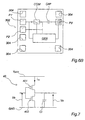
- the integrated circuit of the microcontroller 30 according to the invention has different active parts. These include a part microcontroller interface ⁇ CI and an effective part of treatment of ⁇ CE data shown in Figure 5.
- the micro-controller interface part or micro-interface controller ⁇ CI advantageously comprises only means which consume energy that is not likely to reveal information as to the confidential data processed by the microcontroller.
- the micro-controller interface ⁇ CI includes example a charge pump or interface circuits associated with RST, CLK and I / O pads. With regard to the RST plot, this is including means for detecting an initialization signal and associated means of initialization of the microcontroller. With regard to concerning the CLK pad, it is a means of detecting frequencies between a low limit and a high limit. Finally, with regard to concerning the I / O pad, these are means intended to allow the microcontroller communicate from an input mode to an output mode or vice versa.
- the effective part of data processing or micro-controller effective ⁇ CE is a part of the microcontroller 30 which includes subsets whose inverters are intended for the treatment of confidential data. It is therefore part of the microcontroller likely to give fraudsters information about these confidential data.
- it includes the central unit CPU processing, possibly a cryptoprocessor associated with this unit, data bus and address control circuits as well as RAM, ROM and EEPROM memories or any memories of a Another type.
- the microcontroller 30 also comprises a GEN pulse generator, CAP capacitor and switch COM.
- the pulse generator, the capacity and the switch are means for varying the supply voltage of the microcontroller effective.
- the GEN pulse generator is for example formed of two oscillators consisting, for each of them, of an inverter with hysteresis of Schmitt type on the input circuit, a capacitor connected between the input of the invertor and the ground and a resistor connected between the output of this inverter and its input, said two oscillators being coupled together by a resistor to form a modulated frequency signal source.
- the pulse generator GEN advantageously comprises a synchronization circuit crossing a threshold voltage V threshold of the voltage V ⁇ CE at the terminals of the effective microcontroller.
- This circuit may be formed of a voltage comparator whose positive input is connected to a reference voltage, the threshold voltage V, whose negative input is connected to the voltage at the terminals of the efficient microcontroller, and whose output is connected to the input D of a flip-flop synchronized by the synchronization signal from the modulated frequency signal source.
- CAP capacity has a capacity greater than about 0.1 nanofarad, in particular between about 1 nanofarad and about 10 nanofarads, for example of the order of 6 nanofarads.
- the electrodes with a capacity of 1.5 nanofarad have a surface of the order of 1 mm 2 .
- a capacity of 6 nanofarads has a surface of the order of 4mm 2 .
- the switch COM can be, in the invention, replaced by a variable resistance as a function of time connected in series with the VCC power supply pad of the micro-controller.
- the I / O, RST and CLK pads are connected by electrical connection lines to the microcontroller ⁇ CI interface.
- the GND pad is connected via electrical connection lines to the GEN pulse generator, the CAP capacitor, the efficient ⁇ CE microcontroller and the ⁇ CI microcontroller interface.
- the VCC pad is connected by electrical connection lines to the GEN pulse generator, the COM switch and the ⁇ CI interface microcontroller.
- the COM switch is connected by electrical connection lines to the GEN pulse generator and the CAP capacitor.
- an electrical connection line connects the effective micro-controller ⁇ CE to the electrical connection line connecting the capacitor CAP to the switch COM and an electrical connection line connects the GEN generator to the latter line so as to allow monitoring of the voltage V ⁇ CE for its comparison with the voltage V threshold .
- microcontroller of the type shown in FIG. said elements are arranged in the manner shown in Figs. 6A and 6B in which the complementary layer 302 (FIG. 6B) comprises GEN pulse generator, CAP capacitor and switch COM, and the main layer 301 ( Figure 6A), which carries the pads of contact, includes micro-controller effective parts ⁇ CE and micro-controller ⁇ CI interface.
- the complementary layer 302 comprises GEN pulse generator, CAP capacitor and switch COM
- main layer 301 Figure 6A
- Figure 6A which carries the pads of contact
- the main layer 301 comprises three studs interconnection P1, P2 and P3, a first pad P1 connected to the VCC pad, a second pad P2 connected to the effective microcontroller and a third P3 pad connected to the GND pad.
- the complementary layer 302 comprises three studs interconnection P1 ', P2' and P3 'intended to be placed in the microcontroller, in the vertical view of the studs P1, P2 and P3, respectively.
- the first pad P1 ' is connected, on the one hand, to COM switch and, on the other hand, to the GEN pulse generator, the second pad P2 'is connected to the common point between the switch COM and the capacitance CAP and the third pad P3 'is connected, on the one hand, CAP and the GEN pulse generator.
- the pads P1, P2 and P3 are respectively electrically connected to the pads P1 ', P2' and P3 ' via conductive bosses.
- micro-controller presented above does not constitute that an embodiment according to the invention and it is quite possible to provide other embodiments of micro-controllers do not not showing a layered structure but a structure more classic in which the various elements mentioned above: contact, micro-controllers interface and efficient, capacity, generator pulses and switch, are integrated in a single layer of silicon substrate not covered with a complementary layer.
- the energy Ec ⁇ CI consumed by the microcontroller interface is not indicative of the instructions executed by the microcontroller 30 and therefore not revealing the confidential data involved in the execution of said instructions.
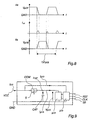
- the elementary gates of the efficient microcontroller are inverters 40 as shown in FIG. 7. These inverters 40 are formed of a P-type transistor 401 connected in series with an N-type transistor 402. The transistor P is brought to FIG. the voltage V ⁇ CE and the transistor N is grounded GND. A capacitor C i is associated with each inverter 40. This capacitance C i is the capacitance equivalent to the physical capacitances of the interconnection lines of the inverter and to the capacitances of the gates forming the transistors P and N of the inverter possibly connected downstream. of the inverter of Figure 7.
- the transistors P and N are controlled by a common control signal V e corresponding to the input voltage of the inverter.
- V e GND
- FIG. 8 shows the variations of the control signal V e , of the intensity of the supply current i cc and of the output signal V s as a function of time t, in the case where the working frequency of the inverter is equal to F ⁇ CE , which is in general the frequency of the clock imposed by the terminal via the pad CLK, but which may be a particular frequency, in the case where the microcontroller is provided with means for generating a clock internal.
- E cc is less than 20% of E d and E s is much smaller than E d .
- the energy E c consumed by the inverter i is mainly dynamic and it is estimated that E c is substantially equal to E d .
- the energy consumed by the efficient microcontroller therefore varies with the square of its supply voltage V ⁇ CE .
- the energy Ec M consumed by the means of the invention is equal to the energy Ec GEN consumed by the pulse generator GEN added to the energy Ec COM consumed by the switch COM and energy Ec CAP consumed by CAP capacity.
- Ec M Ec GEN + Ec COM + Ec CAP
- the energy Ec GEN consumed by the pulse generator GEN is of the same type as the energy consumed by the microcontroller interface. Indeed, it reveals no indication of the confidential data involved in the execution of the instructions.
- the EC COM energy consumed by the COM switch is in fact the energy dissipated by this switch when the capacitor CAP is charging.
- Ec COM Ec CAP during his charge.
- the Ec CAP energy consumed by the CAP capacitor depends on the open or closed state of the COM switch.
- the open or closed state of the switch COM is controlled by the pulse generator GEN. Indeed, this generator is able to send a control signal S to open or close the COM switch. Depending on the signal S received, this switch is closed or open. It is closed during time intervals T on . It is open during time intervals T off.
- a fraudster has access only to the intensity of the supply current of the microcontroller as a whole and consequently only to the energy consumed by the micro-controller as a whole.
- Ec ⁇ CI reveals no information on the switching of the inverters of the effective microcontroller and consequently no information on the confidential data processed. Also, thanks to the invention, the fraudster will not be able to access said data during time intervals T off .
- the energy consumed by the microcontroller is equal to the energy consumed by the microcontroller interface, added to the energy consumed by the means according to the invention and added to the energy consumed by the effective microcontroller.
- Ec C ⁇ Ec .mu.Ci + Ec ⁇ CE + Ec M .
- INS instruction applied to the same OPE operands and executed by the microcontroller according to the invention.
- this INS statement is executed on some clock transitions. AT each clock transition, part of the INS instruction is executed and some of the N inverters of the efficient microcontroller are the subject a change of state for this purpose.
- the energy consumed by the efficient microcontroller during such a transition is directly proportional to the square of the voltage V ⁇ CE at the terminals of said microcontroller.
- the voltage V ⁇ CE at the terminals of the efficient microcontroller is the same as the voltage V CAP across the capacitors CAP. Also, the voltage at the terminals of the efficient microcontroller varies constantly.
- the difference between the energies consumed by the efficient microcontroller is all the greater as they are functions of the square of the supply voltage V ⁇ CE of this microcontroller.
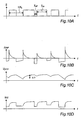
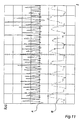
- FIGS. 10A to 10D respectively display the signal S, the current I CAP of the supply current of the capacitor CAP, the voltage V ⁇ CE of the supply of the efficient microcontroller and the intensity of the current Icc of the microphone supply. -controller as a function of time t.
- the cyclic ratio T off / (T on + T off ) thus varies over time and, advantageously, randomly and therefore unpredictable for the fraudster.
- T s due to the manner in which the pulse generator is produced, comprising two oscillators coupled with a Schmitt-type inverter.
- the current I CAP of the capacitor CAP power is positive during the time intervals T on during which the capacitor is charged.
- the capacity is at maximum load when the switch goes to the open state.
- the intensity of the current I CAP is negative in the time intervals T off during which the capacitance is discharged to supply the effective microcontroller.
- the supply voltage V ⁇ CE of the efficient microcontroller increases in the time intervals T on and decreases in the time intervals T off .
- ⁇ V represents the depth of modulation of the voltage across the capacitor.
- the intensity Icc of the supply current of the microcontroller is equal to I ⁇ CI in T off and then increases in T on , where it is equal to I ⁇ CI + I CAP + I ⁇ CE .
- FIG. 11 shows the variations of the intensity of the current Icc as a function of time t, on the one hand, in the case of a microcontroller according to the state of the art (signature A) and, on the other hand , in the case of the same microcontroller according to the invention (signature B) for the execution of identical instructions applied to the same operands.
- signature A the state of the art
- signature B the same microcontroller according to the invention
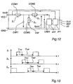
- capacitor CAP1 is discharged to a reference voltage, for example GND, through switch COM3 while switches COM1 and COM2 are open, before being recharged through switch COM1 while the switches COM2 and COM3 are open.
- the CAP1 capacitor once charged through the switch COM1, discharges into the capacitor CAP2 in parallel with the efficient microcontroller ⁇ CE through the switch COM2 while the switches COM1 and COM2 are open.
- FIG. 13 the course of the signals S 1 , S 2 and S 3 has been shown in time.
- the embodiment makes it possible to consume a constant energy independent of the activity of the ⁇ CE. It is no longer possible to obtain confidential information by analyzing the current Icc. This embodiment increases the energy consumption of the efficient microcontroller.
Description
- la figure 1 montre, en perspective, une carte à puce selon l'invention ;
- la figure 2 montre, en coupe transversale, une carte à puce selon l'invention ;
- la figure 3 montre, en vue de face, les plages de contact d'une carte à puce selon l'invention ;
- la figure 4 montre, en perspective, un micro-contrôleur selon l'invention ;
- la figure 5 schématise les différentes parties constitutives d'un micro-contrôleur selon l'invention ;
- la figure 6A représente la couche active du micro-contrôleur selon l'invention montré à la figure 4 ;
- la figure 6B représente la couche complémentaire du micro-contrôleur selon l'invention montré à la figure 4 ;
- la figure 7 schématise un inverseur CMOS d'une partie efficace de traitement des données d'un micro-contrôleur selon l'invention ;
- la figure 8 montre les variations du signal Ve de commande, de l'intensité icc d'alimentation et du signal Vs de sortie de l'inverseur CMOS de la figure 7 en fonction du temps ;
- la figure 9 est un schéma électrique d'un micro-contrôleur selon l'invention ;
- les figures 10A à 10D montrent, respectivement, les variations du signal S, de l'intensité du courant ICAP, de la tension VµCE et de l'intensité Icc du courant d'alimentation d'un micro-contrôleur selon l'invention en fonction du temps ;
- la figure 11 est un enregistrement comparatif des variations de l'intensité Icc du courant en fonction du temps dans le cas d'un micro-contrôleur selon l'état de la technique (signature A) puis dans le cas d'un micro-contrôleur sécurisé selon l'invention (signature B) ;
- la figure 12 est un schéma électrique d'un mode de réalisation particulier d'un micro-contrôleur selon l'invention ; et
- la figure 13 montre les variations des signaux S1, S2 et S3 en fonction du temps, dans le cas d'un micro-contrôleur correspondant au mode de réalisation de la figure 12.
Claims (7)
- Micro-contrôleur (30) destiné à être incorporé dans un objet portatif (1) du type carte à puce, le micro-contrôleur comprenant :caractérisé en ce qu'un circuit d'interface (COM, GEN, CAP) à travers lequel la partie efficace (µCE) reçoit une tension d'alimentation (VµCE), ledit circuit interface (COM, GEN, CAP) étant agencé pour faire varier la tension d'alimentation de la partie efficace de traitement de données (µCE) en modulant le couplage électrique entre le plot de contact (VCC) et la partie efficace (µCE) afin de sécuriser lesdites données confidentielles contre les attaques en courant.un plot de contact (VCC) pour l'alimentation en courant dudit micro-contrôleur (30);un plot (I/O) d'entrée et/ou de sortie de données ;une partie efficace (µCE) pour effectuer un traitement de données, les données comprenant des informations confidentielles ;
- Objet portatif (1) du type carte à puce, comprenant un micro-contrôleur (30) selon la revendication 1.
- Objet portatif du type carte à puce selon la revendication 2 caractérisé en ce que le circuit d'interface comprend :un commutateur (COM) entre ledit plot de contact (VCC) et une borne d'alimentation de la partie efficace de traitement de données (µCE);une capacité (CAP) connectée entre ladite borne d'alimentation ; de la partie efficace du micro-contrôleur (µCE) et une autre borne d'alimentation de la partie efficace (µCE).
- Objet portatif du type carte à puce selon la revendication 3 caractérisé en ce que le circuit d'interface comprend un générateur d'impulsion (GEN) pour contrôler le commutateur (COM) de façon désynchronisée par rapport audit traitement de données.
- Objet portatif du type carte à puce selon la revendication 4 ou la revendication 3 caractérisé en ce que la capacité a une capacité supérieure à 1 nanofarad.
- Objet portatif du type carte à puce selon la revendication 2 caractérisé en ce que le micro-contrôleur comporte une couche principale (301) de silicium dont la face active, qui intègre un circuit et porte les plots (300) de contact, est scellée à une couche complémentaire (302) de protection au moyen d'une couche de scellement (303).
- Objet portatif du type carte à puce selon la revendication 6 caractérisé en ce que ledit circuit d'interface (COM, GEN, CAP) est situé dans la couche complémentaire de protection (302).
Applications Claiming Priority (3)
| Application Number | Priority Date | Filing Date | Title |
|---|---|---|---|
| FR9909555 | 1999-07-22 | ||
| FR9909555A FR2796738B1 (fr) | 1999-07-22 | 1999-07-22 | Micro-controleur securise contre les attaques en courant |
| PCT/FR2000/002058 WO2001008088A1 (fr) | 1999-07-22 | 2000-07-17 | Micro-controleur securise contre les attaques en courant |
Publications (2)
| Publication Number | Publication Date |
|---|---|
| EP1204948A1 EP1204948A1 (fr) | 2002-05-15 |
| EP1204948B1 true EP1204948B1 (fr) | 2004-02-25 |
Family
ID=9548428
Family Applications (1)
| Application Number | Title | Priority Date | Filing Date |
|---|---|---|---|
| EP00953248A Expired - Lifetime EP1204948B1 (fr) | 1999-07-22 | 2000-07-17 | Micro-controleur securise contre les attaques en courant |
Country Status (8)
| Country | Link |
|---|---|
| US (1) | US6848619B1 (fr) |
| EP (1) | EP1204948B1 (fr) |
| JP (1) | JP4769398B2 (fr) |
| CN (1) | CN1183483C (fr) |
| AT (1) | ATE260494T1 (fr) |
| DE (1) | DE60008544T9 (fr) |
| FR (1) | FR2796738B1 (fr) |
| WO (1) | WO2001008088A1 (fr) |
Cited By (3)
| Publication number | Priority date | Publication date | Assignee | Title |
|---|---|---|---|---|
| US7668310B2 (en) | 1998-06-03 | 2010-02-23 | Cryptography Research, Inc. | Cryptographic computation using masking to prevent differential power analysis and other attacks |
| US7941666B2 (en) | 1998-07-02 | 2011-05-10 | Cryptography Research, Inc. | Payment smart cards with hierarchical session key derivation providing security against differential power analysis and other attacks |
| US8879724B2 (en) | 1998-01-02 | 2014-11-04 | Rambus Inc. | Differential power analysis—resistant cryptographic processing |
Families Citing this family (18)
| Publication number | Priority date | Publication date | Assignee | Title |
|---|---|---|---|---|
| FR2811790A1 (fr) * | 2000-07-11 | 2002-01-18 | Schlumberger Systems & Service | Microcontroleur securise contre des attaques dites en courant |
| JP3977592B2 (ja) * | 2000-12-28 | 2007-09-19 | 株式会社東芝 | データ処理装置 |
| FR2822988B1 (fr) | 2001-04-02 | 2003-08-15 | Oberthur Card Syst Sa | Procede de protection d'une entite electronique a microcircuit et entite electronique dotee d'une telle protection |
| DE10162309A1 (de) | 2001-12-19 | 2003-07-03 | Philips Intellectual Property | Verfahren und Anordnung zur Erhöhung der Sicherheit von Schaltkreisen gegen unbefugten Zugriff |
| GB0221240D0 (en) * | 2002-09-13 | 2002-10-23 | Koninkl Philips Electronics Nv | Current source for cryptographic processor |
| DE10245747B4 (de) * | 2002-10-01 | 2005-12-01 | Infineon Technologies Ag | Kontaktloser Datenträger |
| EP1486908A1 (fr) * | 2003-06-12 | 2004-12-15 | Axalto S.A. | Carte à puce avec deux ports d'entrée/sortie pour la connexion des environnements sécurisés et non sécurisés |
| WO2004111857A2 (fr) * | 2003-06-17 | 2004-12-23 | Philips Intellectual Property & Standards Gmbh | Microcontroleur et methode d'adressage |
| FR2870406A1 (fr) | 2004-05-14 | 2005-11-18 | St Microelectronics Sa | Modulation de charge d'un transporteur |
| BRPI0721441B1 (pt) * | 2007-03-12 | 2018-10-30 | Incard Sa | método e aparelho para detectar correlações entre padrões de sinal |
| EP2235874A1 (fr) | 2007-12-13 | 2010-10-06 | Nxp B.V. | Circuit électronique et procédé de masquage d'exigences de courant d'un circuit électronique |
| JP5482048B2 (ja) * | 2009-09-18 | 2014-04-23 | ソニー株式会社 | 集積回路および電子機器 |
| FR2953960B1 (fr) * | 2009-12-14 | 2012-01-13 | Oberthur Technologies | Composant electronique apte a detecter des attaques par apport d'energie |
| US8635467B2 (en) | 2011-10-27 | 2014-01-21 | Certicom Corp. | Integrated circuit with logic circuitry and multiple concealing circuits |
| US8334705B1 (en) | 2011-10-27 | 2012-12-18 | Certicom Corp. | Analog circuitry to conceal activity of logic circuitry |
| US10210350B2 (en) | 2015-08-10 | 2019-02-19 | Samsung Electronics Co., Ltd. | Electronic device against side channel attacks |
| FR3061580A1 (fr) * | 2017-01-03 | 2018-07-06 | Stmicroelectronics (Rousset) Sas | Procede et dispositif de gestion de la consommation en courant d'un module integre. |
| FR3073645A1 (fr) | 2017-11-13 | 2019-05-17 | Stmicroelectronics (Rousset) Sas | Procede de modification aleatoire du profil de consommation d'un circuit logique, et dispositif associe |
Family Cites Families (25)
| Publication number | Priority date | Publication date | Assignee | Title |
|---|---|---|---|---|
| US3911202A (en) * | 1973-01-31 | 1975-10-07 | Moore & Co Samuel | Electron cured plastic insulated conductors |
| US3843829A (en) * | 1973-03-02 | 1974-10-22 | Bendix Corp | Center strength member cable |
| FR2535488B1 (fr) * | 1982-10-29 | 1988-06-17 | Thomson Csf | Objet portatif electronique pour le stockage d'informations |
| JPS62105293A (ja) * | 1985-10-31 | 1987-05-15 | Toshiba Corp | 携帯可能記録媒体の読取・書込装置 |
| FR2604554B1 (fr) * | 1986-09-30 | 1988-11-10 | Eurotechnique Sa | Dispositif de securite pourla programmation d'une memoire non volatile programmable electriquement |
| US4860343A (en) * | 1986-12-22 | 1989-08-22 | Zetena Jr Maurice F | Composite cable for use in high frequency data and voice transmission |
| FR2638869B1 (fr) * | 1988-11-10 | 1990-12-21 | Sgs Thomson Microelectronics | Dispositif de securite contre la detection non autorisee de donnees protegees |
| JPH0738188B2 (ja) * | 1989-10-17 | 1995-04-26 | 三菱電機株式会社 | マイクロコンピュータ及びこれを用いた非接触icカード |
| US5037999A (en) * | 1990-03-08 | 1991-08-06 | W. L. Gore & Associates | Conductively-jacketed coaxial cable |
| US5149915A (en) * | 1991-06-06 | 1992-09-22 | Molex Incorporated | Hybrid shielded cable |
| US5744757A (en) * | 1995-03-28 | 1998-04-28 | Belden Wire & Cable Company | Plenum cable |
| US5486649A (en) * | 1994-03-17 | 1996-01-23 | Belden Wire & Cable Company | Shielded cable |
| US5956445A (en) * | 1994-05-20 | 1999-09-21 | Belden Wire & Cable Company | Plenum rated cables and shielding tape |
| US5574250A (en) * | 1995-02-03 | 1996-11-12 | W. L. Gore & Associates, Inc. | Multiple differential pair cable |
| US5767442A (en) * | 1995-12-22 | 1998-06-16 | Amphenol Corporation | Non-skew cable assembly and method of making the same |
| US6164550A (en) * | 1995-12-22 | 2000-12-26 | Thomson Licensing S.A. | Fault detection and modification circuit |
| FR2743647B1 (fr) * | 1996-01-12 | 1998-02-13 | Bull Cp8 | Coupleur pour gerer une communication entre un support de donnees portable et un dispositif d'echange de donnees, et dispositif d'echange de donnees associe |
| US6010788A (en) * | 1997-12-16 | 2000-01-04 | Tensolite Company | High speed data transmission cable and method of forming same |
| US6403887B1 (en) * | 1997-12-16 | 2002-06-11 | Tensolite Company | High speed data transmission cable and method of forming same |
| EP0964361A1 (fr) * | 1998-06-08 | 1999-12-15 | International Business Machines Corporation | Protection d'information sensible contenue dans les cartes à puce |
| US6594760B1 (en) * | 1998-12-21 | 2003-07-15 | Pitney Bowes Inc. | System and method for suppressing conducted emissions by a cryptographic device |
| DE19907575A1 (de) * | 1999-02-23 | 2000-08-24 | Philips Corp Intellectual Pty | Schaltungsanordnung zum Liefern eines Speisestromes |
| JP3827050B2 (ja) * | 1999-03-09 | 2006-09-27 | 株式会社ルネサステクノロジ | Icカードと半導体集積回路装置 |
| US6419159B1 (en) * | 1999-06-14 | 2002-07-16 | Microsoft Corporation | Integrated circuit device with power analysis protection circuitry |
| FR2800490B1 (fr) * | 1999-11-02 | 2002-01-04 | Sagem | Procede pour assurer l'inviolabilite d'un micromodule de carte a puce contre une analyse de sa consommation de courant et micromodule agence pour sa mise en oeuvre |
-
1999
- 1999-07-22 FR FR9909555A patent/FR2796738B1/fr not_active Expired - Fee Related
-
2000
- 2000-07-17 DE DE60008544T patent/DE60008544T9/de active Active
- 2000-07-17 EP EP00953248A patent/EP1204948B1/fr not_active Expired - Lifetime
- 2000-07-17 JP JP2001513101A patent/JP4769398B2/ja not_active Expired - Lifetime
- 2000-07-17 US US10/031,681 patent/US6848619B1/en not_active Expired - Lifetime
- 2000-07-17 WO PCT/FR2000/002058 patent/WO2001008088A1/fr active IP Right Grant
- 2000-07-17 AT AT00953248T patent/ATE260494T1/de not_active IP Right Cessation
- 2000-07-17 CN CNB008124728A patent/CN1183483C/zh not_active Expired - Lifetime
Cited By (6)
| Publication number | Priority date | Publication date | Assignee | Title |
|---|---|---|---|---|
| US8879724B2 (en) | 1998-01-02 | 2014-11-04 | Rambus Inc. | Differential power analysis—resistant cryptographic processing |
| US9419790B2 (en) | 1998-01-02 | 2016-08-16 | Cryptography Research, Inc. | Differential power analysis—resistant cryptographic processing |
| US7668310B2 (en) | 1998-06-03 | 2010-02-23 | Cryptography Research, Inc. | Cryptographic computation using masking to prevent differential power analysis and other attacks |
| US7787620B2 (en) | 1998-06-03 | 2010-08-31 | Cryptography Research, Inc. | Prevention of side channel attacks against block cipher implementations and other cryptographic systems |
| US7941666B2 (en) | 1998-07-02 | 2011-05-10 | Cryptography Research, Inc. | Payment smart cards with hierarchical session key derivation providing security against differential power analysis and other attacks |
| US9852572B2 (en) | 1998-07-02 | 2017-12-26 | Cryptography Research, Inc. | Cryptographic token with leak-resistant key derivation |
Also Published As
| Publication number | Publication date |
|---|---|
| FR2796738A1 (fr) | 2001-01-26 |
| EP1204948A1 (fr) | 2002-05-15 |
| WO2001008088A1 (fr) | 2001-02-01 |
| FR2796738B1 (fr) | 2001-09-14 |
| DE60008544T2 (de) | 2004-12-23 |
| JP2003505797A (ja) | 2003-02-12 |
| ATE260494T1 (de) | 2004-03-15 |
| DE60008544T9 (de) | 2005-05-04 |
| CN1183483C (zh) | 2005-01-05 |
| US6848619B1 (en) | 2005-02-01 |
| DE60008544D1 (de) | 2004-04-01 |
| JP4769398B2 (ja) | 2011-09-07 |
| CN1372676A (zh) | 2002-10-02 |
Similar Documents
| Publication | Publication Date | Title |
|---|---|---|
| EP1204948B1 (fr) | Micro-controleur securise contre les attaques en courant | |
| EP2108164B1 (fr) | Limitation d'acces a une ressource d'un circuit electronique | |
| EP0270410B1 (fr) | Circuit intégré du type circuit logique comportant une mémoire non volatile programmable électriquement | |
| WO2008084016A1 (fr) | Protection d'informations contenues dans un circuit electronique | |
| FR2533047A1 (fr) | Carte a memoire avec un circuit integre incorpore | |
| FR2851065A1 (fr) | Cartes a microprocesseur ayant des circuits de protection qui empechent des attaques par analyse de puissance, et procedes pour les faire fonctionner | |
| EP1293856A1 (fr) | Circuit Intégré sécurisé comprenant des parties à caractère confidentiel, et procédé pour sa mise en action | |
| FR2904464A1 (fr) | Circuit eeprom de retention de charges pour mesure temporelle | |
| EP2162846A2 (fr) | Cryptoprocesseur a protection de donnees amelioree | |
| EP0965994B1 (fr) | Dispositif à circuit intégré sécurisé au moyen de lignes complémentaires de bus | |
| EP0750244B1 (fr) | Circuit générateur de tension négative du type pompe de charge | |
| WO1999013572A1 (fr) | Generateur d'alea | |
| EP0323367B1 (fr) | Circuit de remise sous tension pour circuit intégré en technologie MOS | |
| EP1053531B1 (fr) | Dispositif a circuit integre securise par attenuation de signatures electriques | |
| FR2811790A1 (fr) | Microcontroleur securise contre des attaques dites en courant | |
| CA2212951C (fr) | Connecteur pour appareil lecteur de carte a microcircuit | |
| FR2768532A1 (fr) | Carte a puce presentant des logos electroniquement actifs | |
| EP3353704A1 (fr) | Dispositif de protection d'un circuit électronique avec détection d'un changement de réactance électrique | |
| EP0678868B1 (fr) | Circuit multiplicateur de tension | |
| FR2534751A1 (fr) | Circuit de restauration a la mise sous tension pour un systeme de commande electrique | |
| EP1317701A1 (fr) | Procede de brouillage de la consommation electrique d'un circuit integre | |
| EP3876138A1 (fr) | Procédé d'écriture de données dans une mémoire d'un transpondeur sans contact, et dispositif de transpondeur sans contact correspondant | |
| FR3041455A1 (fr) | Systeme de detection d'intrusions par reconfiguration | |
| FR2810438A1 (fr) | Circuit de detection d'usure | |
| WO2004029873A1 (fr) | Entite electronique securisee avec gestion du temps |
Legal Events
| Date | Code | Title | Description |
|---|---|---|---|
| PUAI | Public reference made under article 153(3) epc to a published international application that has entered the european phase |
Free format text: ORIGINAL CODE: 0009012 |
|
| 17P | Request for examination filed |
Effective date: 20020221 |
|
| AK | Designated contracting states |
Kind code of ref document: A1 Designated state(s): AT BE CH CY DE DK ES FI FR GB GR IE IT LI LU MC NL PT SE |
|
| 17Q | First examination report despatched |
Effective date: 20020611 |
|
| GRAP | Despatch of communication of intention to grant a patent |
Free format text: ORIGINAL CODE: EPIDOSNIGR1 |
|
| GRAS | Grant fee paid |
Free format text: ORIGINAL CODE: EPIDOSNIGR3 |
|
| GRAA | (expected) grant |
Free format text: ORIGINAL CODE: 0009210 |
|
| AK | Designated contracting states |
Kind code of ref document: B1 Designated state(s): AT BE CH CY DE DK ES FI FR GB GR IE IT LI LU MC NL PT SE |
|
| PG25 | Lapsed in a contracting state [announced via postgrant information from national office to epo] |
Ref country code: AT Free format text: LAPSE BECAUSE OF FAILURE TO SUBMIT A TRANSLATION OF THE DESCRIPTION OR TO PAY THE FEE WITHIN THE PRESCRIBED TIME-LIMIT Effective date: 20040225 Ref country code: IE Free format text: LAPSE BECAUSE OF FAILURE TO SUBMIT A TRANSLATION OF THE DESCRIPTION OR TO PAY THE FEE WITHIN THE PRESCRIBED TIME-LIMIT Effective date: 20040225 Ref country code: NL Free format text: LAPSE BECAUSE OF FAILURE TO SUBMIT A TRANSLATION OF THE DESCRIPTION OR TO PAY THE FEE WITHIN THE PRESCRIBED TIME-LIMIT Effective date: 20040225 Ref country code: CY Free format text: LAPSE BECAUSE OF FAILURE TO SUBMIT A TRANSLATION OF THE DESCRIPTION OR TO PAY THE FEE WITHIN THE PRESCRIBED TIME-LIMIT Effective date: 20040225 Ref country code: FI Free format text: LAPSE BECAUSE OF FAILURE TO SUBMIT A TRANSLATION OF THE DESCRIPTION OR TO PAY THE FEE WITHIN THE PRESCRIBED TIME-LIMIT Effective date: 20040225 |
|
| REG | Reference to a national code |
Ref country code: GB Ref legal event code: FG4D Free format text: NOT ENGLISH |
|
| REG | Reference to a national code |
Ref country code: CH Ref legal event code: EP |
|
| REG | Reference to a national code |
Ref country code: IE Ref legal event code: FG4D Free format text: FRENCH |
|
| REF | Corresponds to: |
Ref document number: 60008544 Country of ref document: DE Date of ref document: 20040401 Kind code of ref document: P |
|
| PG25 | Lapsed in a contracting state [announced via postgrant information from national office to epo] |
Ref country code: GR Free format text: LAPSE BECAUSE OF FAILURE TO SUBMIT A TRANSLATION OF THE DESCRIPTION OR TO PAY THE FEE WITHIN THE PRESCRIBED TIME-LIMIT Effective date: 20040525 Ref country code: SE Free format text: LAPSE BECAUSE OF FAILURE TO SUBMIT A TRANSLATION OF THE DESCRIPTION OR TO PAY THE FEE WITHIN THE PRESCRIBED TIME-LIMIT Effective date: 20040525 Ref country code: DK Free format text: LAPSE BECAUSE OF FAILURE TO SUBMIT A TRANSLATION OF THE DESCRIPTION OR TO PAY THE FEE WITHIN THE PRESCRIBED TIME-LIMIT Effective date: 20040525 |
|
| PG25 | Lapsed in a contracting state [announced via postgrant information from national office to epo] |
Ref country code: ES Free format text: LAPSE BECAUSE OF FAILURE TO SUBMIT A TRANSLATION OF THE DESCRIPTION OR TO PAY THE FEE WITHIN THE PRESCRIBED TIME-LIMIT Effective date: 20040605 |
|
| GBT | Gb: translation of ep patent filed (gb section 77(6)(a)/1977) |
Effective date: 20040617 |
|
| PG25 | Lapsed in a contracting state [announced via postgrant information from national office to epo] |
Ref country code: LU Free format text: LAPSE BECAUSE OF NON-PAYMENT OF DUE FEES Effective date: 20040717 |
|
| PG25 | Lapsed in a contracting state [announced via postgrant information from national office to epo] |
Ref country code: BE Free format text: LAPSE BECAUSE OF NON-PAYMENT OF DUE FEES Effective date: 20040731 Ref country code: MC Free format text: LAPSE BECAUSE OF NON-PAYMENT OF DUE FEES Effective date: 20040731 Ref country code: LI Free format text: LAPSE BECAUSE OF NON-PAYMENT OF DUE FEES Effective date: 20040731 Ref country code: CH Free format text: LAPSE BECAUSE OF NON-PAYMENT OF DUE FEES Effective date: 20040731 |
|
| NLV1 | Nl: lapsed or annulled due to failure to fulfill the requirements of art. 29p and 29m of the patents act | ||
| REG | Reference to a national code |
Ref country code: IE Ref legal event code: FD4D |
|
| RAP2 | Party data changed (patent owner data changed or rights of a patent transferred) |
Owner name: AXALTO S.A. |
|
| PLBE | No opposition filed within time limit |
Free format text: ORIGINAL CODE: 0009261 |
|
| STAA | Information on the status of an ep patent application or granted ep patent |
Free format text: STATUS: NO OPPOSITION FILED WITHIN TIME LIMIT |
|
| BERE | Be: lapsed |
Owner name: *SCHLUMBERGER SYSTEMES Effective date: 20040731 |
|
| 26N | No opposition filed |
Effective date: 20041126 |
|
| REG | Reference to a national code |
Ref country code: CH Ref legal event code: PL |
|
| REG | Reference to a national code |
Ref country code: FR Ref legal event code: CA Ref country code: FR Ref legal event code: CD |
|
| BERE | Be: lapsed |
Owner name: *SCHLUMBERGER SYSTEMES Effective date: 20040731 |
|
| PG25 | Lapsed in a contracting state [announced via postgrant information from national office to epo] |
Ref country code: PT Free format text: LAPSE BECAUSE OF NON-PAYMENT OF DUE FEES Effective date: 20040725 |
|
| REG | Reference to a national code |
Ref country code: DE Ref legal event code: R082 Ref document number: 60008544 Country of ref document: DE |
|
| REG | Reference to a national code |
Ref country code: DE Ref legal event code: R081 Ref document number: 60008544 Country of ref document: DE Owner name: GEMALTO SA, FR Free format text: FORMER OWNER: AXALTO S.A., MONTROUGE, FR Effective date: 20111013 |
|
| REG | Reference to a national code |
Ref country code: FR Ref legal event code: PLFP Year of fee payment: 17 |
|
| REG | Reference to a national code |
Ref country code: FR Ref legal event code: PLFP Year of fee payment: 18 |
|
| REG | Reference to a national code |
Ref country code: FR Ref legal event code: PLFP Year of fee payment: 19 |
|
| PGFP | Annual fee paid to national office [announced via postgrant information from national office to epo] |
Ref country code: IT Payment date: 20190624 Year of fee payment: 20 |
|
| PGFP | Annual fee paid to national office [announced via postgrant information from national office to epo] |
Ref country code: FR Payment date: 20190621 Year of fee payment: 20 |
|
| PGFP | Annual fee paid to national office [announced via postgrant information from national office to epo] |
Ref country code: DE Payment date: 20190620 Year of fee payment: 20 Ref country code: GB Payment date: 20190624 Year of fee payment: 20 |
|
| REG | Reference to a national code |
Ref country code: DE Ref legal event code: R071 Ref document number: 60008544 Country of ref document: DE |
|
| REG | Reference to a national code |
Ref country code: GB Ref legal event code: PE20 Expiry date: 20200716 |
|
| PG25 | Lapsed in a contracting state [announced via postgrant information from national office to epo] |
Ref country code: GB Free format text: LAPSE BECAUSE OF EXPIRATION OF PROTECTION Effective date: 20200716 |