EP0989538A2 - Verfahren zur Ansteuerung einer Plasmaanzeigetafel und Einrichtung zur Durchführung des Verfahrens - Google Patents
Verfahren zur Ansteuerung einer Plasmaanzeigetafel und Einrichtung zur Durchführung des Verfahrens Download PDFInfo
- Publication number
- EP0989538A2 EP0989538A2 EP99300996A EP99300996A EP0989538A2 EP 0989538 A2 EP0989538 A2 EP 0989538A2 EP 99300996 A EP99300996 A EP 99300996A EP 99300996 A EP99300996 A EP 99300996A EP 0989538 A2 EP0989538 A2 EP 0989538A2
- Authority
- EP
- European Patent Office
- Prior art keywords
- voltage
- reset
- discharge
- electrodes
- sustaining discharge
- Prior art date
- Legal status (The legal status is an assumption and is not a legal conclusion. Google has not performed a legal analysis and makes no representation as to the accuracy of the status listed.)
- Withdrawn
Links
Images


Classifications
-
- G—PHYSICS
- G09—EDUCATION; CRYPTOGRAPHY; DISPLAY; ADVERTISING; SEALS
- G09G—ARRANGEMENTS OR CIRCUITS FOR CONTROL OF INDICATING DEVICES USING STATIC MEANS TO PRESENT VARIABLE INFORMATION
- G09G3/00—Control arrangements or circuits, of interest only in connection with visual indicators other than cathode-ray tubes
- G09G3/20—Control arrangements or circuits, of interest only in connection with visual indicators other than cathode-ray tubes for presentation of an assembly of a number of characters, e.g. a page, by composing the assembly by combination of individual elements arranged in a matrix no fixed position being assigned to or needed to be assigned to the individual characters or partial characters
- G09G3/22—Control arrangements or circuits, of interest only in connection with visual indicators other than cathode-ray tubes for presentation of an assembly of a number of characters, e.g. a page, by composing the assembly by combination of individual elements arranged in a matrix no fixed position being assigned to or needed to be assigned to the individual characters or partial characters using controlled light sources
- G09G3/28—Control arrangements or circuits, of interest only in connection with visual indicators other than cathode-ray tubes for presentation of an assembly of a number of characters, e.g. a page, by composing the assembly by combination of individual elements arranged in a matrix no fixed position being assigned to or needed to be assigned to the individual characters or partial characters using controlled light sources using luminous gas-discharge panels, e.g. plasma panels
- G09G3/288—Control arrangements or circuits, of interest only in connection with visual indicators other than cathode-ray tubes for presentation of an assembly of a number of characters, e.g. a page, by composing the assembly by combination of individual elements arranged in a matrix no fixed position being assigned to or needed to be assigned to the individual characters or partial characters using controlled light sources using luminous gas-discharge panels, e.g. plasma panels using AC panels
- G09G3/291—Control arrangements or circuits, of interest only in connection with visual indicators other than cathode-ray tubes for presentation of an assembly of a number of characters, e.g. a page, by composing the assembly by combination of individual elements arranged in a matrix no fixed position being assigned to or needed to be assigned to the individual characters or partial characters using controlled light sources using luminous gas-discharge panels, e.g. plasma panels using AC panels controlling the gas discharge to control a cell condition, e.g. by means of specific pulse shapes
-
- G—PHYSICS
- G09—EDUCATION; CRYPTOGRAPHY; DISPLAY; ADVERTISING; SEALS
- G09G—ARRANGEMENTS OR CIRCUITS FOR CONTROL OF INDICATING DEVICES USING STATIC MEANS TO PRESENT VARIABLE INFORMATION
- G09G3/00—Control arrangements or circuits, of interest only in connection with visual indicators other than cathode-ray tubes
- G09G3/20—Control arrangements or circuits, of interest only in connection with visual indicators other than cathode-ray tubes for presentation of an assembly of a number of characters, e.g. a page, by composing the assembly by combination of individual elements arranged in a matrix no fixed position being assigned to or needed to be assigned to the individual characters or partial characters
- G09G3/2007—Display of intermediate tones
- G09G3/2018—Display of intermediate tones by time modulation using two or more time intervals
- G09G3/2022—Display of intermediate tones by time modulation using two or more time intervals using sub-frames
-
- G—PHYSICS
- G09—EDUCATION; CRYPTOGRAPHY; DISPLAY; ADVERTISING; SEALS
- G09G—ARRANGEMENTS OR CIRCUITS FOR CONTROL OF INDICATING DEVICES USING STATIC MEANS TO PRESENT VARIABLE INFORMATION
- G09G3/00—Control arrangements or circuits, of interest only in connection with visual indicators other than cathode-ray tubes
- G09G3/20—Control arrangements or circuits, of interest only in connection with visual indicators other than cathode-ray tubes for presentation of an assembly of a number of characters, e.g. a page, by composing the assembly by combination of individual elements arranged in a matrix no fixed position being assigned to or needed to be assigned to the individual characters or partial characters
- G09G3/22—Control arrangements or circuits, of interest only in connection with visual indicators other than cathode-ray tubes for presentation of an assembly of a number of characters, e.g. a page, by composing the assembly by combination of individual elements arranged in a matrix no fixed position being assigned to or needed to be assigned to the individual characters or partial characters using controlled light sources
- G09G3/28—Control arrangements or circuits, of interest only in connection with visual indicators other than cathode-ray tubes for presentation of an assembly of a number of characters, e.g. a page, by composing the assembly by combination of individual elements arranged in a matrix no fixed position being assigned to or needed to be assigned to the individual characters or partial characters using controlled light sources using luminous gas-discharge panels, e.g. plasma panels
- G09G3/288—Control arrangements or circuits, of interest only in connection with visual indicators other than cathode-ray tubes for presentation of an assembly of a number of characters, e.g. a page, by composing the assembly by combination of individual elements arranged in a matrix no fixed position being assigned to or needed to be assigned to the individual characters or partial characters using controlled light sources using luminous gas-discharge panels, e.g. plasma panels using AC panels
- G09G3/291—Control arrangements or circuits, of interest only in connection with visual indicators other than cathode-ray tubes for presentation of an assembly of a number of characters, e.g. a page, by composing the assembly by combination of individual elements arranged in a matrix no fixed position being assigned to or needed to be assigned to the individual characters or partial characters using controlled light sources using luminous gas-discharge panels, e.g. plasma panels using AC panels controlling the gas discharge to control a cell condition, e.g. by means of specific pulse shapes
- G09G3/292—Control arrangements or circuits, of interest only in connection with visual indicators other than cathode-ray tubes for presentation of an assembly of a number of characters, e.g. a page, by composing the assembly by combination of individual elements arranged in a matrix no fixed position being assigned to or needed to be assigned to the individual characters or partial characters using controlled light sources using luminous gas-discharge panels, e.g. plasma panels using AC panels controlling the gas discharge to control a cell condition, e.g. by means of specific pulse shapes for reset discharge, priming discharge or erase discharge occurring in a phase other than addressing
- G09G3/2927—Details of initialising
-
- G—PHYSICS
- G09—EDUCATION; CRYPTOGRAPHY; DISPLAY; ADVERTISING; SEALS
- G09G—ARRANGEMENTS OR CIRCUITS FOR CONTROL OF INDICATING DEVICES USING STATIC MEANS TO PRESENT VARIABLE INFORMATION
- G09G3/00—Control arrangements or circuits, of interest only in connection with visual indicators other than cathode-ray tubes
- G09G3/20—Control arrangements or circuits, of interest only in connection with visual indicators other than cathode-ray tubes for presentation of an assembly of a number of characters, e.g. a page, by composing the assembly by combination of individual elements arranged in a matrix no fixed position being assigned to or needed to be assigned to the individual characters or partial characters
- G09G3/22—Control arrangements or circuits, of interest only in connection with visual indicators other than cathode-ray tubes for presentation of an assembly of a number of characters, e.g. a page, by composing the assembly by combination of individual elements arranged in a matrix no fixed position being assigned to or needed to be assigned to the individual characters or partial characters using controlled light sources
- G09G3/28—Control arrangements or circuits, of interest only in connection with visual indicators other than cathode-ray tubes for presentation of an assembly of a number of characters, e.g. a page, by composing the assembly by combination of individual elements arranged in a matrix no fixed position being assigned to or needed to be assigned to the individual characters or partial characters using controlled light sources using luminous gas-discharge panels, e.g. plasma panels
- G09G3/288—Control arrangements or circuits, of interest only in connection with visual indicators other than cathode-ray tubes for presentation of an assembly of a number of characters, e.g. a page, by composing the assembly by combination of individual elements arranged in a matrix no fixed position being assigned to or needed to be assigned to the individual characters or partial characters using controlled light sources using luminous gas-discharge panels, e.g. plasma panels using AC panels
- G09G3/291—Control arrangements or circuits, of interest only in connection with visual indicators other than cathode-ray tubes for presentation of an assembly of a number of characters, e.g. a page, by composing the assembly by combination of individual elements arranged in a matrix no fixed position being assigned to or needed to be assigned to the individual characters or partial characters using controlled light sources using luminous gas-discharge panels, e.g. plasma panels using AC panels controlling the gas discharge to control a cell condition, e.g. by means of specific pulse shapes
- G09G3/294—Control arrangements or circuits, of interest only in connection with visual indicators other than cathode-ray tubes for presentation of an assembly of a number of characters, e.g. a page, by composing the assembly by combination of individual elements arranged in a matrix no fixed position being assigned to or needed to be assigned to the individual characters or partial characters using controlled light sources using luminous gas-discharge panels, e.g. plasma panels using AC panels controlling the gas discharge to control a cell condition, e.g. by means of specific pulse shapes for lighting or sustain discharge
-
- G—PHYSICS
- G09—EDUCATION; CRYPTOGRAPHY; DISPLAY; ADVERTISING; SEALS
- G09G—ARRANGEMENTS OR CIRCUITS FOR CONTROL OF INDICATING DEVICES USING STATIC MEANS TO PRESENT VARIABLE INFORMATION
- G09G3/00—Control arrangements or circuits, of interest only in connection with visual indicators other than cathode-ray tubes
- G09G3/20—Control arrangements or circuits, of interest only in connection with visual indicators other than cathode-ray tubes for presentation of an assembly of a number of characters, e.g. a page, by composing the assembly by combination of individual elements arranged in a matrix no fixed position being assigned to or needed to be assigned to the individual characters or partial characters
- G09G3/22—Control arrangements or circuits, of interest only in connection with visual indicators other than cathode-ray tubes for presentation of an assembly of a number of characters, e.g. a page, by composing the assembly by combination of individual elements arranged in a matrix no fixed position being assigned to or needed to be assigned to the individual characters or partial characters using controlled light sources
- G09G3/28—Control arrangements or circuits, of interest only in connection with visual indicators other than cathode-ray tubes for presentation of an assembly of a number of characters, e.g. a page, by composing the assembly by combination of individual elements arranged in a matrix no fixed position being assigned to or needed to be assigned to the individual characters or partial characters using controlled light sources using luminous gas-discharge panels, e.g. plasma panels
- G09G3/288—Control arrangements or circuits, of interest only in connection with visual indicators other than cathode-ray tubes for presentation of an assembly of a number of characters, e.g. a page, by composing the assembly by combination of individual elements arranged in a matrix no fixed position being assigned to or needed to be assigned to the individual characters or partial characters using controlled light sources using luminous gas-discharge panels, e.g. plasma panels using AC panels
- G09G3/296—Driving circuits for producing the waveforms applied to the driving electrodes
-
- G—PHYSICS
- G09—EDUCATION; CRYPTOGRAPHY; DISPLAY; ADVERTISING; SEALS
- G09G—ARRANGEMENTS OR CIRCUITS FOR CONTROL OF INDICATING DEVICES USING STATIC MEANS TO PRESENT VARIABLE INFORMATION
- G09G2320/00—Control of display operating conditions
- G09G2320/02—Improving the quality of display appearance
- G09G2320/0228—Increasing the driving margin in plasma displays
-
- G—PHYSICS
- G09—EDUCATION; CRYPTOGRAPHY; DISPLAY; ADVERTISING; SEALS
- G09G—ARRANGEMENTS OR CIRCUITS FOR CONTROL OF INDICATING DEVICES USING STATIC MEANS TO PRESENT VARIABLE INFORMATION
- G09G2320/00—Control of display operating conditions
- G09G2320/02—Improving the quality of display appearance
- G09G2320/0238—Improving the black level
Definitions
- the present invention relates to a method of driving a plasma display panel (PDP) of three-electrode AC type, and in particular to a technique for resetting each cell of the PDP to a predetermined state.
- PDP plasma display panel
- the AC-type PDP continues to discharge and emit light for display in accordance with a voltage waveform applied alternately to two sustaining electrodes thereof. Each session of discharge is completed within 1 ⁇ s to several ⁇ s from the pulse application.
- the ions that are the positive charge generated by the discharge are accumulated on the surface of an insulating layer on an electrode supplied with a negative voltage.
- the electrons which are negative charge are accumulated on the surface of an insulating layer on an electrode supplied with a positive voltage.
- a wall charge is initially generated by a discharge with a pulse (write pulse) of a high voltage, followed by application of a pulse (a sustaining pulse or a sustaining discharge pulse) of a voltage (sustaining voltage or a sustaining discharge voltage) lower than and having a different polarity from the preceding voltage, then the pulse is superposed on the wall charge previously accumulated, and increases the voltage of the discharge space to such an extent that the discharge starts over a threshold value of the discharge voltage.
- a cell once gaining a wall charge by a write discharge, sustains the discharge when supplied with alternate sustaining pulses of opposite polarities. This is called the memory effect or the memory function.
- the AC-type PDP uses this memory effect for display.
- the AC-type PDP is of two types, one a two-electrode type in which selective discharge (addressing discharge) and sustaining discharge are carried out with two electrodes, and the other a three-electrode type in which a third electrode is used for addressing discharge.
- the phosphor material formed in the discharge cell is excited by the ultraviolet light generated by the discharge.
- the disadvantage of this phosphor material is that it easily succumbs to the impact of ions making up the positive charge generated at the same time as the discharge.
- the PDP of a two-electrode type is so configured that the phosphor material comes into direct contact with ions, which is liable to shorten the life of the phosphor material.
- the color PDP generally uses the three-electrode structure utilizing the surface discharge.
- the PDP of three-electrode type is further classified into a configuration in which the third electrode is formed on the same substrate that the first and second electrodes for sustaining discharge are arranged on and a configuration in which the third electrode is arranged on the other substrate in opposed relation to the first substrate.
- the configuration in which three electrodes are formed on the same substrate is also subdivided into a configuration in which a third electrode is arranged on the two electrodes for sustaining discharge and a configuration in which a third electrode is arranged under the other two electrodes.
- the visible light emitted from the phosphor material is either transmitted through the phosphor material (transmission type) or reflected from the phosphor material (reflection type).
- An embodiment of the present invention can be applied to the three-electrode AC-type PDP.
- An explanation will be given with reference to the reflection type of PDP comprising a panel including a third electrode formed on a substrate in opposed relation to the substrate of the sustaining discharge electrodes, in which a part of the sustaining electrode is formed of a transparent electrode.
- each subfield is configured of a reset period, an addressing period and a sustaining discharge period, and a self-erasure discharge is caused by applying a reset pulse of high voltage so that all the cells discharge during the reset period.
- the light emission by the application of the reset pulse and the light emission by self-erasure discharge also contribute to the display.
- the light emission at all the cells regardless of the specific contents of the display increases the background brightness for a reduced contrast.
- each frame is segmented into a plurality of subfields, and the frequency of the sustaining discharge in each subfield is changed in accordance with the weight of the brightness.
- the sustaining discharge is effected only several times. The light emission at all the cells, therefore, deteriorates the linearity of gradation display.
- the display quality of the PDP apparatus has been improved to such an extent that the deterioration of display quality due to the fact described above has begun to pose a problem.
- An embodiment of a first aspect of the present invention can provide a method of driving a plasma display panel, in which the voltage of the reset pulse is set taking into consideration the voltage due to the charge accumulated in accordance with the display, so that the self-erasure discharge is caused not in all the cells but only in the cells involved in display.
- the self-erasure discharge like the sustaining discharge, the display brightness is set as a discharge involved in display.
- An embodiment of a second aspect of the present invention can provide a method of driving a plasma display panel comprising a plurality of pairs of first and second electrodes arranged in parallel, and a plurality of third electrodes crossed with the pairs of the first and second electrodes, wherein a plurality of cells adapted to discharge and emit light are determined selectively by the first, second and third electrodes, comprising the steps of causing the self-erasure discharge by applying a reset voltage to at least a part of the first, second and third electrodes and thereby causing a plurality of cells to discharge, and neutralizing the charge of the electrodes thereby to set a plurality of cells in a predetermined state (reset step), applying a voltage in accordance with the display data to each cell in the predetermined state and accumulating the charged corresponding to the display data for each cell (addressing step), and applying a sustaining discharge voltage to a plurality of cells and causing the cells having a predetermined charge accumulated therein to discharge and emit light (sustaining discharge step), the reset voltage being set in
- the self-erasure discharge in the reset step occurs only in the cells that have discharged in the sustaining discharge step.
- the discharge by the reset pulse and the resulting self-erasure discharge are carried out only in the cells to be displayed. Therefore, the resulting light emission does not increase the background brightness and therefore the contrast is not reduced.
- the display brightness is set also for the charge by the reset pulse and the resulting self-erasure discharge as a discharge involved in display like the sustaining discharge, the linearity of the gradation display is maintained.
- the time of application of the reset voltage for the second and subsequent reset steps is shortened as compared with the application time of the other sustaining discharge voltages thereby to neutralize the charge without accumulation of the wall charge.
- a voltage sufficiently smaller than another reset voltage opposite in polarity to the first reset pulse can be applied after complete application of the first reset pulse.
- the self-erasure discharge occurs due to the wall charge accumulated by the reset pulse.
- the self-erasure discharge is more positively caused. In the process, the wall charge is not accumulated if the voltage of opposite polarity is sufficiently lower than the reset voltage.
- the self-erasure discharge is not caused simply by the wall charge accumulated by the sustaining discharge. Even in the case where a pulse of a low voltage, opposite in polarity to the immediately-preceding sustaining discharge voltage, is applied as a reset pulse, however, the discharge occurs once the sum of the low reset pulse voltage and the voltage due to the wall charge reaches a level not lower than the discharge starting voltage. At this time, the wall charge is not accumulated if the reset pulse voltage is low.
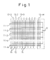
- Fig. 1 is a plan view schematically showing a three-electrode AC-type PDP
- Fig. 2 is a (vertical) sectional view schematically showing a discharge cell of the panel shown in Fig. 1
- Fig. 3 is a (horizontal) sectional view schematically showing the cell.
- each component part having the same function will be designated by the same reference numeral.
- the two glass substrates are assembled with the ridges of the barriers 14 and the surface of the Mg0 film closely contacting each other.
- the space between the phosphor members 27 and the Mg0 film surface 25 constitutes a discharge space 26.
- Fig. 4 is a block diagram schematically showing peripheral circuits for driving the PDP of Figs. 1 to 3.
- the Y driver 101 includes a Y scan driver 102 and a Y common driver 103, and the Y electrodes are connected individually to the Y scan driver 102.
- the Y scan driver 102 is connected to the Y common driver 103.
- the pulses for addressing discharge are generated by the Y scan driver 102, while the sustaining pulses and the like are generated by the Y common driver 103 and, through the Y scan driver 102, applied to the Y electrodes.
- the X electrodes 12 are connected to all the display lines of the panel and led out as a common electrode.
- the X common driver 104 generates a write pulse, a sustaining pulse and the like.
- the gradation of the PDP is displayed by setting each bit of the display data to a corresponding subfield period and changing the length of the subfield period in accordance with the weight of the bit.
- the display data are given by 8 bits, one frame is displayed in eight subfield periods and each bit data is displayed in each of the subfield periods.
- the subfield period has a length of 1, 2, 4, 8, 16, 32, 64 or 128.
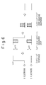
- Fiq. 5 is a waveform diagram showing a previously-considered method of driving the PDP of Figs. 1 to 3 by the circuit of Fig. 4.
- These drive waveforms of the prior art represent what is called "the write addressing method of addressing/sustaining charge period separation type".
- one subfield is segmented into a reset period, an addressing period and a sustaining discharge period.
- the reset period all the Y electrodes are reset to 0 V level.
- the full surface write pulse of a high voltage about 330 V
- the potential of the addressing electrodes is about 100 V.
- the addressing discharge is effected line by line during the addressing period in order to turn on/off the cells in accordance with the display data.
- a predetermined voltage about 50 V
- a scan pulse about -150 V
- Addressing pulses about 50 V are applied selectively to the addressing electrodes corresponding to the cells adapted to develop a sustaining discharge i.e. the addressing electrodes associated with the cells to be turned on.
- a discharge occurs between the Y electrodes and the addressing electrodes of the cells to be turned on.
- the discharge occurs between the X electrodes and the Y electrodes, so that the wall charge of an amount permitting the sustaining discharge is accumulated on the MgO film surface of the two electrodes.
- a predetermined voltage about -50 V for preventing discharge is applied to the Y electrodes not supplied with the scan pulse.
- a similar operation is also performed sequentially for other display lines, and thus new display data are written over all the display lines.
- the X and Y electrodes are supplied with a sustaining pulse (about 180 V) alternately and conduct the sustaining discharge to display an image for one subfield.
- a sustaining pulse about 180 V
- the wall charge is accumulated between the X and Y electrodes of the display cells during the addressing period, and the voltage due to this wall charge is superposed on the sustaining pulse to cause the discharge. No wall charge is accumulated on the cells not displayed. These cells develop no discharge even when supplied with a sustaining pulse.
- an addressing voltage of about 100 V is applied to the addressing electrode in order to avoid the discharge between the addressing electrode and the X or Y electrodes.
- the brightness is determined by the length of the sustaining discharge period, i.e. the frequency of the sustaining pulses.
- the positive charge accumulated on the Y electrodes increases the potential of the Y electrodes by ⁇ VY, while the charge accumulated on the X electrodes decreases the potential of the X electrodes by ⁇ VX.
- the potential of the X electrodes becomes VX1 - ⁇ VX
- the potential of the Y electrodes becomes ⁇ VY.
- the voltage between X and Y electrodes thus assumes VX1 - ⁇ VX - ⁇ VY.
- the voltage of the pulse for the full surface write which is applied to the X electrodes during the reset period is so high that a large amount of wall charge is accumulated on the X and Y electrodes at the time point when the discharge stops.
- the corresponding absolute values of ⁇ VX and ⁇ VY are also large.
- the X and Y electrodes are reduced to 0 V, the self-erasure discharge occurs and the wall charge is neutralized.
- only a small sustaining charge voltage is applied to the X and Y electrodes during the sustaining discharge period.
- the voltage obtained by superposing the charge accumulated by selective discharge during the addressing period is set to a value slightly higher than the discharge starting voltage. Therefore, at the time point when the discharge by each sustaining discharge pulse stops, only a small amount of wall charge is accumulated on the X and Y electrodes. No discharge occurs, therefore, even when the X and Y electrodes are set to 0 V.
- a self-erasure discharge is caused by applying a reset pulse which is so high that all the cells discharge during the reset period.
- the light emission due to the application of a reset pulse or the light emission due to the self-erasure discharge reduces the contrast and hence the linearity of gradation display.
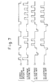
- the PDP apparatus of this embodiment has a similar configuration to the previously-considered one described with reference to Figs. 1 to 5, except for the self-erasure pulse. Only the different parts will be explained below.
- Fig. 7 is a diagram showing various drive waveforms for the PDP apparatus according to the first embodiment. As compared with Fig. 5, this embodiment is apparently different from the previously-considered apparatus in that the voltage of the last sustaining discharge pulse during the sustaining discharge period of each subfield is higher than other sustaining discharge pulses and the second and subsequent reset pulses are removed.
- the voltage of the last sustaining discharge pulse is higher than the voltage of other sustaining discharge pulses during the sustaining discharge period of each subfield.
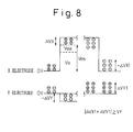
- the self-erasure discharge due to the last sustaining discharge pulse will be explained with reference to Fig. 8.
- the voltage ⁇ VX + ⁇ VY between the X and Y electrodes at this time is not higher than the discharge starting voltage, and therefore no discharge occurs.
- the sustaining discharge pulse of voltage Vs is applied to the X electrodes thereby to develop a sustaining discharge.
- the wall charges equivalent to the voltages ⁇ VX and ⁇ VY were stored again on the X and Y electrodes.
- This pulse is higher than the sustaining discharge pulse by Vea, and therefore the discharge naturally occurs.
- the negative wall charge is accumulated on the X electrodes
- the positive wall charge is accumulated on the Y electrodes, thus stopping the discharge.
- the wall charge is accumulated in a greater amount than during other sustaining discharge periods.
- - ⁇ VX1 be the voltage due to the negative wall charge accumulated on the X electrodes
- ⁇ VY1 be the voltage due to the positive wall charge accumulated on the Y electrodes.
- the voltage ⁇ VX1 + ⁇ VY1 between the X and Y electrodes is higher than the discharge starting voltage.
- the voltage Ves is set to a level where no discharge occurs even if a reset pulse is applied to the cells formed with no wall charge for lack of the sustaining discharge.
- the discharge by the reset pulses occurs only in the cells which have been subjected to sustaining discharge to emit light. No wall discharge is accumulated on the electrodes of the cells not discharged upon application of a reset pulse thereto, and therefore such cells remain in the same state as if reset.
- the discharge by the reset pulse and the resulting self-erasure discharge occur only in the cells intended for display. Therefore, the resulting light emission does not increase the background brightness and the contrast is not reduced. Further, in the case where the display brightness is set by considering the discharge due to the reset pulse and the self-erasure discharge associated therewith as discharges associated with the display, the linearity for gradation display can be maintained.
- the last sustaining discharge pulse applied to the X electrodes is defined as a reset pulse. Nevertheless, the last sustaining discharge pulse, if applied to the Y electrodes, can also be used as a reset pulse.
- Fig. 9A shows a circuit configuration of a Y common drive 103 and an X common driver 104 for realizing the drive waveforms according to the first embodiment
- Fig. 9B shows the voltage waveforms applied to the X and Y electrodes and the operation of the switches.
- this circuit includes a sustaining discharge voltage source for outputting a sustaining discharge voltage Vs, a first reset voltage source for outputting a voltage Vw of a first reset pulse, a second reset voltage source for outputting second and subsequent reset voltages Ves, and a grounding terminal.
- the X electrode is connected to the sustaining discharge voltage source through a switch SW1, to the grounding terminal through a switch SW2, to the first reset voltage source through a switch SW5, and to the second reset voltage source through a switch SW6.
- the Y electrode is connected to the sustaining discharge voltage source through a switch SW3 and to the grounding terminal through a switch SW4.
- the X and Y electrodes are supplied with voltages as shown in Fig. 9B during the reset period and the sustaining discharge period from the Y command driver 103 and the X common driver 104, respectively.
- Each switch operates as shown in order to apply the above-mentioned voltages.
- Each switch is in the on state at a "high" H signal state and is in the off state at a "low” L signal state.
- Fig. 10A shows another circuit configuration of the Y common driver 103 and the X common driver 104 for realizing the drive waveforms according to the first embodiment.
- Fig. 10B shows the voltage waveforms applied to the X and Y electrodes and the operation of each switch.
- this circuit includes a sustaining discharge voltage source for outputting the sustaining discharge voltage Vs, a first reset difference voltage source for outputting a difference voltage Vwa between the first reset pulse voltage Vw and the sustaining discharge voltage Vs, a second reset difference voltage source for outputting a difference voltage Vea between the second and subsequent reset pulse voltage Ves and the sustaining discharge voltage Vs, and a grounding terminal.
- a diode D, a capacitor C and three switches SW15 to SW17 makes up a voltage superposition circuit for switching the output between the sustaining discharge voltage Vs to the switch SW11, the sustaining discharge voltage Vs superposed with the first difference voltage Vwa (i.e.
- the switches SW11 to SW14 have the same function as the switches SW1 to SW4 of Fig. 9A, respectively.
- the anode of the diode D is connected to a sustaining discharge voltage source, and the cathode is connected to one terminal of a terminal of the capacitor C and the switch SW11.
- the other end of the capacitor C is connected through the switch SW15 to the first reset difference voltage source, to a second reset difference voltage through the switch SW16, and to the grounding terminal through the switch SW17.
- the fifth switch SW15 and the sixth switch SW16 are turned off and the seventh switch SW17 is turned on.
- the capacitor C is charged to the sustaining voltage Vs across it.
- the sixth switch SW16 and the seventh switch SW17 are turned off while the fifth switch 15 is turned on.
- the other end of the capacitor C is supplied with the voltage Vwa, and therefore the voltage at an end of the capacitor C increases by the voltage Vs and assumes Vs + Vwa, i.e. the voltage Vw.
- the switch SW11 is turned on and the voltage Vw is applied to the X electrodes.
- the fifth switch SW15 and the sixth switch SW16 are turned off while the seventh switch SW17 is turned on.
- the sustaining discharge voltage Vs is output from the switch SW11.
- the fifth switch SW15 and the sixth switch SW16 are turned off while the seventh switch SW17 is turned on.
- the fifth switch SW15 and the seventh switch SW17 are turned off while the sixth switch SW16 is turned on.
- the other end of the capacitor C is supplied with the voltage Vea.
- the voltage Vs held is added to the voltage at an end of the capacitor C.
- the capacitor C assumes a voltage Vs + Vea, i.e. Ves.
- the switch SW11 thus is turned on and the voltage Vw is applied to the X electrodes.
- the voltage of the last sustaining discharge pulse is increased beyond the other sustaining discharge pulses to ensure the occurrence of the self-erasure discharge when the two electrodes are set at the same potential upon complete application of the last sustaining discharge pulse.
- the voltage of the last sustaining discharge pulse is desirably as high as possible. Once the voltage of the last sustaining discharge pulse exceeds the discharge starting voltage, however, even those cells that have not accumulated the wall charge and have not developed the sustaining discharge begin to discharge. Therefore, the voltage of the last sustaining discharge voltage cannot be increased beyond the discharge starting voltage.
- the self-erasure discharge cannot occur unless the voltage of the last sustaining discharge pulse is increased beyond the discharge starting voltage, therefore, the conditions for realizing the first embodiment of the present invention are lacking.
- the second embodiment described below is an example in which the self-erasure discharge is positively caused even under such conditions.
- Fig. 11 is a diagram showing drive waveforms of the PDP apparatus according to the second embodiment of the invention.
- both the X and Y electrodes are set to the potential of 0 V after the last sustaining discharge pulse is applied to the X electrodes.
- the Y electrodes are supplied with a small positive voltage (several tens of volts), i.e. a pulse of a small voltage opposite in polarity to the last sustaining discharge pulse.
- a small positive voltage severe tens of volts
- the negative wall charge accumulates on the X electrodes and the positive wall charge accumulates on the Y electrodes.
- the pulse of the small voltage of opposite polarity therefore, is superposed on the wall charge thereby to increase the voltages of the X and Y electrodes.
- the application of the small voltage of opposite polarity can start the self-erasure discharge. Even when the accumulated wall charge is sufficient to start the self-erasure discharge, positive occurrence of the self-erasure discharge is assured.
- the small pulse of opposite polarity thus added has so small a voltage that only a very small amount of the wall charge is accumulated after the discharge starts, and can be regarded substantially as a self-erasure discharge.
- Fig. 12 is a diagram showing drive waveforms of the PDP apparatus according to a third embodiment of the invention.
- all the sustaining discharge pulses like in the previously-considered apparatus as shown in Fig. 5, have the same voltage, and the self-erasure discharge is not activated even after complete application of the sustaining discharge pulse.
- a pulse of small voltage opposite in polarity to the last sustaining discharge pulse is applied.
- this small voltage of opposite polarity is superposed on the wall charge and increases the voltage between the X and Y electrodes.
- the applied pulse of opposite polarity is so small that the amount of the wall charge accumulating after the discharge starts is very small and the charge can be regarded substantially as a self-erasure discharge.
- Fig. 13 is a diagram showing drive waveforms of the PDP apparatus according to a fourth embodiment of the invention.
- all the sustaining discharg pulses assume the same voltage, although the last sustaining discharge pulse is shorter in width.
- the first reset pulse though as high as to cause the discharge of all the cells, is shorter in width.
- the self-erasure discharge is realized by neutralization without accumulating the wall charge.
- the cells that emit light by sustaining discharge develop the self-erasure discharge upon application thereto of the last sustaining discharge voltage.
Applications Claiming Priority (2)
| Application Number | Priority Date | Filing Date | Title |
|---|---|---|---|
| JP25682598 | 1998-09-10 | ||
| JP10256825A JP2000089720A (ja) | 1998-09-10 | 1998-09-10 | プラズマディスプレイの駆動方法及びプラズマディスプレイ装置 |
Publications (2)
| Publication Number | Publication Date |
|---|---|
| EP0989538A2 true EP0989538A2 (de) | 2000-03-29 |
| EP0989538A3 EP0989538A3 (de) | 2000-11-22 |
Family
ID=17297963
Family Applications (1)
| Application Number | Title | Priority Date | Filing Date |
|---|---|---|---|
| EP99300996A Withdrawn EP0989538A3 (de) | 1998-09-10 | 1999-02-11 | Verfahren zur Ansteuerung einer Plasmaanzeigetafel und Einrichtung zur Durchführung des Verfahrens |
Country Status (5)
| Country | Link |
|---|---|
| US (1) | US6087779A (de) |
| EP (1) | EP0989538A3 (de) |
| JP (1) | JP2000089720A (de) |
| KR (1) | KR100341218B1 (de) |
| TW (1) | TW419640B (de) |
Cited By (4)
| Publication number | Priority date | Publication date | Assignee | Title |
|---|---|---|---|---|
| EP1199701A2 (de) * | 2000-08-30 | 2002-04-24 | Fujitsu Hitachi Plasma Display Limited | Plasmaanzeigetafel mit verbessertem Kontrast |
| FR2822577A1 (fr) * | 2001-03-23 | 2002-09-27 | Samsung Sdi Co Ltd | Procede et dispositif pour piloter un panneau d'affichage a plasma dans lequel une decharge de reinitialisation est executee selectivement |
| EP1324302A2 (de) | 2001-10-10 | 2003-07-02 | Lg Electronics Inc. | Plasmabildanzeigevorrichtung und Steuerungsverfahren hierzu |
| EP1524642A2 (de) * | 2003-10-16 | 2005-04-20 | Pioneer Corporation | Anzeigevorrichtung |
Families Citing this family (14)
| Publication number | Priority date | Publication date | Assignee | Title |
|---|---|---|---|---|
| KR100598182B1 (ko) * | 1999-07-23 | 2006-07-10 | 엘지전자 주식회사 | 플라즈마 디스플레이 패널 및 이 패널의 구동 방법과 장치 |
| JP3736672B2 (ja) * | 2000-05-25 | 2006-01-18 | パイオニア株式会社 | プラズマディスプレイパネルの駆動方法 |
| KR20020019670A (ko) * | 2000-09-06 | 2002-03-13 | 김순택 | 플라즈마 표시 패널의 구동 방법 |
| KR100349924B1 (ko) * | 2000-10-13 | 2002-08-24 | 삼성에스디아이 주식회사 | 플라즈마 표시패널의 구동방법 |
| JP2002169507A (ja) * | 2000-11-30 | 2002-06-14 | Fujitsu Ltd | プラズマディスプレイパネル及びその駆動方法 |
| KR100445027B1 (ko) * | 2001-03-23 | 2004-08-18 | 삼성에스디아이 주식회사 | 선택적 리셋방전을 수행하는 플라즈마 디스플레이 패널의구동방법 및 그 장치 |
| JP4675517B2 (ja) * | 2001-07-24 | 2011-04-27 | 株式会社日立製作所 | プラズマディスプレイ装置 |
| KR100475158B1 (ko) * | 2002-04-04 | 2005-03-08 | 엘지전자 주식회사 | 플라즈마 디스플레이 패널의 구동방법 |
| KR100467694B1 (ko) * | 2002-05-23 | 2005-01-24 | 삼성에스디아이 주식회사 | 효과적으로 초기화 단계들이 수행되는 플라즈마디스플레이 패널의 구동 방법 |
| KR100467431B1 (ko) * | 2002-07-23 | 2005-01-24 | 삼성에스디아이 주식회사 | 플라즈마 디스플레이 패널 및 그 구동 방법 |
| EP1471491A3 (de) * | 2003-04-22 | 2005-03-23 | Samsung SDI Co., Ltd. | Plasmabildschirm und Ansteuerverfahren dafür |
| KR100515341B1 (ko) * | 2003-09-02 | 2005-09-15 | 삼성에스디아이 주식회사 | 플라즈마 디스플레이 패널의 구동 장치 |
| KR100550983B1 (ko) * | 2003-11-26 | 2006-02-13 | 삼성에스디아이 주식회사 | 플라즈마 표시 장치 및 플라즈마 표시 패널의 구동 방법 |
| KR100608886B1 (ko) * | 2003-12-31 | 2006-08-03 | 엘지전자 주식회사 | 플라즈마 디스플레이 패널의 구동방법 및 장치 |
Citations (4)
| Publication number | Priority date | Publication date | Assignee | Title |
|---|---|---|---|---|
| EP0549275A1 (de) * | 1991-12-20 | 1993-06-30 | Fujitsu Limited | Verfahren und Vorrichtung zur Steuerung einer Anzeigetafel |
| EP0680067A2 (de) * | 1994-04-28 | 1995-11-02 | Matsushita Electronics Corporation | Gasentladungs-Anzeigegerät und Verfahren zur Steuerung desselben |
| FR2744276A1 (fr) * | 1996-01-31 | 1997-08-01 | Fujitsu Ltd | Dispositif d'affichage a panneau d'affichage par plasma, son procede d'excitation, et un generateur d'onde utilise avec celui-ci |
| EP0855692A1 (de) * | 1997-01-28 | 1998-07-29 | Nec Corporation | Verfahren zur Ansteuerung einer Plasma-Anzeigetafel |
Family Cites Families (5)
| Publication number | Priority date | Publication date | Assignee | Title |
|---|---|---|---|---|
| JP2772753B2 (ja) * | 1993-12-10 | 1998-07-09 | 富士通株式会社 | プラズマディスプレイパネル並びにその駆動方法及び駆動回路 |
| JP3555995B2 (ja) * | 1994-10-31 | 2004-08-18 | 富士通株式会社 | プラズマディスプレイ装置 |
| JP3499058B2 (ja) * | 1995-09-13 | 2004-02-23 | 富士通株式会社 | プラズマディスプレイの駆動方法及びプラズマディスプレイ装置 |
| JPH0981074A (ja) * | 1995-09-19 | 1997-03-28 | Fujitsu Ltd | ディスプレイ装置及びディスプレイユニット及びディスプレイ信号生成装置 |
| JP3704813B2 (ja) * | 1996-06-18 | 2005-10-12 | 三菱電機株式会社 | プラズマディスプレイパネルの駆動方法及びプラズマディスプレイ |
-
1998
- 1998-09-10 JP JP10256825A patent/JP2000089720A/ja active Pending
-
1999
- 1999-02-10 TW TW088102089A patent/TW419640B/zh not_active IP Right Cessation
- 1999-02-11 EP EP99300996A patent/EP0989538A3/de not_active Withdrawn
- 1999-02-11 US US09/248,107 patent/US6087779A/en not_active Expired - Fee Related
- 1999-03-05 KR KR1019990007297A patent/KR100341218B1/ko not_active IP Right Cessation
Patent Citations (4)
| Publication number | Priority date | Publication date | Assignee | Title |
|---|---|---|---|---|
| EP0549275A1 (de) * | 1991-12-20 | 1993-06-30 | Fujitsu Limited | Verfahren und Vorrichtung zur Steuerung einer Anzeigetafel |
| EP0680067A2 (de) * | 1994-04-28 | 1995-11-02 | Matsushita Electronics Corporation | Gasentladungs-Anzeigegerät und Verfahren zur Steuerung desselben |
| FR2744276A1 (fr) * | 1996-01-31 | 1997-08-01 | Fujitsu Ltd | Dispositif d'affichage a panneau d'affichage par plasma, son procede d'excitation, et un generateur d'onde utilise avec celui-ci |
| EP0855692A1 (de) * | 1997-01-28 | 1998-07-29 | Nec Corporation | Verfahren zur Ansteuerung einer Plasma-Anzeigetafel |
Non-Patent Citations (1)
| Title |
|---|
| SANO Y ET AL: "A FULL-COLOR SURFACE-DISCHARGE AC PLASMA TV DISPLAY" SID INTERNATIONAL SYMPOSIUM DIGEST OF TECHNICAL PAPERS,US,PLAYA DEL REY, SID, vol. 22, 6 May 1991 (1991-05-06), pages 728-731, XP000503118 ISSN: 0097-966X * |
Cited By (11)
| Publication number | Priority date | Publication date | Assignee | Title |
|---|---|---|---|---|
| EP1199701A2 (de) * | 2000-08-30 | 2002-04-24 | Fujitsu Hitachi Plasma Display Limited | Plasmaanzeigetafel mit verbessertem Kontrast |
| EP1199701A3 (de) * | 2000-08-30 | 2006-03-29 | Fujitsu Hitachi Plasma Display Limited | Plasmaanzeigetafel mit verbessertem Kontrast |
| FR2822577A1 (fr) * | 2001-03-23 | 2002-09-27 | Samsung Sdi Co Ltd | Procede et dispositif pour piloter un panneau d'affichage a plasma dans lequel une decharge de reinitialisation est executee selectivement |
| GB2373913A (en) * | 2001-03-23 | 2002-10-02 | Samsung Sdi Co Ltd | Method for driving plasma display panel in which reset discharge is selectively performed |
| GB2373913B (en) * | 2001-03-23 | 2005-10-12 | Samsung Sdi Co Ltd | Method and apparatus for driving plasma dispaly panel in which reset discharge is selectively performed |
| US7173578B2 (en) | 2001-03-23 | 2007-02-06 | Samsung Sdi Co., Ltd. | Method and apparatus for driving a plasma display panel in which reset discharge is selectively performed |
| EP1324302A2 (de) | 2001-10-10 | 2003-07-02 | Lg Electronics Inc. | Plasmabildanzeigevorrichtung und Steuerungsverfahren hierzu |
| EP1324302A3 (de) * | 2001-10-10 | 2004-11-03 | Lg Electronics Inc. | Plasmabildanzeigevorrichtung und Steuerungsverfahren hierzu |
| US6956331B2 (en) | 2001-10-10 | 2005-10-18 | Lg Electronics Inc. | Plasma display panel and driving method thereof |
| EP1524642A2 (de) * | 2003-10-16 | 2005-04-20 | Pioneer Corporation | Anzeigevorrichtung |
| EP1524642A3 (de) * | 2003-10-16 | 2005-06-22 | Pioneer Corporation | Anzeigevorrichtung |
Also Published As
| Publication number | Publication date |
|---|---|
| JP2000089720A (ja) | 2000-03-31 |
| KR100341218B1 (ko) | 2002-06-21 |
| KR20000022590A (ko) | 2000-04-25 |
| EP0989538A3 (de) | 2000-11-22 |
| TW419640B (en) | 2001-01-21 |
| US6087779A (en) | 2000-07-11 |
Similar Documents
| Publication | Publication Date | Title |
|---|---|---|
| US6087779A (en) | Method of driving plasma display and plasma display apparatus using the method | |
| US6034482A (en) | Method and apparatus for driving plasma display panel | |
| KR100354678B1 (ko) | 플라즈마 디스플레이 패널의 구동방법 | |
| KR100807488B1 (ko) | 플라즈마 디스플레이 장치의 구동 방법 | |
| JP3429438B2 (ja) | Ac型pdpの駆動方法 | |
| US20060061521A1 (en) | Method and apparatus of driving plasma display panel | |
| JPH10207417A (ja) | プラズマディスプレイパネルの駆動方法、プラズマディスプレイパネル及び表示装置 | |
| JP2002278510A (ja) | プラズマディスプレイパネルの駆動方法および表示装置 | |
| JP2000020021A (ja) | プラズマディスプレイパネル駆動方法 | |
| JPH0968946A (ja) | 画像表示装置、および画像表示装置の駆動方法 | |
| JP4349501B2 (ja) | プラズマディスプレイパネルの駆動方法 | |
| JP4530048B2 (ja) | プラズマディスプレイ装置およびプラズマディスプレイパネルの駆動方法 | |
| EP1739648B1 (de) | Plasmaanzeigevorrichtung und Verfahren zu ihrer Ansteuerung | |
| JP3630640B2 (ja) | プラズマディスプレイパネルおよびその駆動方法 | |
| US7489287B2 (en) | Method and apparatus for resetting a plasma display panel | |
| US20080316147A1 (en) | Methods for resetting and driving plasma display panels in which address electrode lines are electrically floated | |
| JP2000305513A (ja) | プラズマディスプレイパネルの駆動装置および駆動方法 | |
| KR100432648B1 (ko) | 유지 방전 특성을 개선한 플라즈마 디스플레이 패널의구동 장치 및 그 구동 방법 | |
| JP4725522B2 (ja) | プラズマディスプレイパネルの駆動方法およびプラズマディスプレイ装置 | |
| JP2002189443A (ja) | プラズマディスプレイパネルの駆動方法 | |
| JP4332585B2 (ja) | プラズマディスプレイパネルの駆動方法 | |
| US20050219155A1 (en) | Driving method of display panel | |
| US20020044107A1 (en) | Method of driving a plasma display panel, and a plasma display apparatus using the method | |
| JP4223541B2 (ja) | プラズマディスプレイパネルの駆動方法 | |
| JP3662239B2 (ja) | プラズマディスプレイ装置の駆動方法 |
Legal Events
| Date | Code | Title | Description |
|---|---|---|---|
| PUAI | Public reference made under article 153(3) epc to a published international application that has entered the european phase |
Free format text: ORIGINAL CODE: 0009012 |
|
| AK | Designated contracting states |
Kind code of ref document: A2 Designated state(s): DE FR |
|
| AX | Request for extension of the european patent |
Free format text: AL;LT;LV;MK;RO;SI |
|
| PUAL | Search report despatched |
Free format text: ORIGINAL CODE: 0009013 |
|
| AK | Designated contracting states |
Kind code of ref document: A3 Designated state(s): AT BE CH CY DE DK ES FI FR GB GR IE IT LI LU MC NL PT SE |
|
| AX | Request for extension of the european patent |
Free format text: AL;LT;LV;MK;RO;SI |
|
| 17P | Request for examination filed |
Effective date: 20010305 |
|
| AKX | Designation fees paid |
Free format text: DE FR |
|
| RAP1 | Party data changed (applicant data changed or rights of an application transferred) |
Owner name: HITACHI, LTD. |
|
| 17Q | First examination report despatched |
Effective date: 20060921 |
|
| RAP1 | Party data changed (applicant data changed or rights of an application transferred) |
Owner name: HITACHI PLASMA PATENT LICENSING CO., LTD. |
|
| STAA | Information on the status of an ep patent application or granted ep patent |
Free format text: STATUS: THE APPLICATION IS DEEMED TO BE WITHDRAWN |
|
| 18D | Application deemed to be withdrawn |
Effective date: 20070202 |