EP0984424A1 - Liquid crystal display device - Google Patents
Liquid crystal display device Download PDFInfo
- Publication number
- EP0984424A1 EP0984424A1 EP99402162A EP99402162A EP0984424A1 EP 0984424 A1 EP0984424 A1 EP 0984424A1 EP 99402162 A EP99402162 A EP 99402162A EP 99402162 A EP99402162 A EP 99402162A EP 0984424 A1 EP0984424 A1 EP 0984424A1
- Authority
- EP
- European Patent Office
- Prior art keywords
- potential
- time
- signal
- liquid crystal
- crystal display
- Prior art date
- Legal status (The legal status is an assumption and is not a legal conclusion. Google has not performed a legal analysis and makes no representation as to the accuracy of the status listed.)
- Ceased
Links
Images


Classifications
-
- G—PHYSICS
- G09—EDUCATION; CRYPTOGRAPHY; DISPLAY; ADVERTISING; SEALS
- G09G—ARRANGEMENTS OR CIRCUITS FOR CONTROL OF INDICATING DEVICES USING STATIC MEANS TO PRESENT VARIABLE INFORMATION
- G09G3/00—Control arrangements or circuits, of interest only in connection with visual indicators other than cathode-ray tubes
- G09G3/20—Control arrangements or circuits, of interest only in connection with visual indicators other than cathode-ray tubes for presentation of an assembly of a number of characters, e.g. a page, by composing the assembly by combination of individual elements arranged in a matrix no fixed position being assigned to or needed to be assigned to the individual characters or partial characters
- G09G3/34—Control arrangements or circuits, of interest only in connection with visual indicators other than cathode-ray tubes for presentation of an assembly of a number of characters, e.g. a page, by composing the assembly by combination of individual elements arranged in a matrix no fixed position being assigned to or needed to be assigned to the individual characters or partial characters by control of light from an independent source
- G09G3/36—Control arrangements or circuits, of interest only in connection with visual indicators other than cathode-ray tubes for presentation of an assembly of a number of characters, e.g. a page, by composing the assembly by combination of individual elements arranged in a matrix no fixed position being assigned to or needed to be assigned to the individual characters or partial characters by control of light from an independent source using liquid crystals
- G09G3/3611—Control of matrices with row and column drivers
- G09G3/3685—Details of drivers for data electrodes
- G09G3/3688—Details of drivers for data electrodes suitable for active matrices only
-
- G—PHYSICS
- G09—EDUCATION; CRYPTOGRAPHY; DISPLAY; ADVERTISING; SEALS
- G09G—ARRANGEMENTS OR CIRCUITS FOR CONTROL OF INDICATING DEVICES USING STATIC MEANS TO PRESENT VARIABLE INFORMATION
- G09G2310/00—Command of the display device
- G09G2310/02—Addressing, scanning or driving the display screen or processing steps related thereto
- G09G2310/0264—Details of driving circuits
- G09G2310/0297—Special arrangements with multiplexing or demultiplexing of display data in the drivers for data electrodes, in a pre-processing circuitry delivering display data to said drivers or in the matrix panel, e.g. multiplexing plural data signals to one D/A converter or demultiplexing the D/A converter output to multiple columns
-
- G—PHYSICS
- G09—EDUCATION; CRYPTOGRAPHY; DISPLAY; ADVERTISING; SEALS
- G09G—ARRANGEMENTS OR CIRCUITS FOR CONTROL OF INDICATING DEVICES USING STATIC MEANS TO PRESENT VARIABLE INFORMATION
- G09G2320/00—Control of display operating conditions
- G09G2320/02—Improving the quality of display appearance
- G09G2320/0209—Crosstalk reduction, i.e. to reduce direct or indirect influences of signals directed to a certain pixel of the displayed image on other pixels of said image, inclusive of influences affecting pixels in different frames or fields or sub-images which constitute a same image, e.g. left and right images of a stereoscopic display
-
- G—PHYSICS
- G09—EDUCATION; CRYPTOGRAPHY; DISPLAY; ADVERTISING; SEALS
- G09G—ARRANGEMENTS OR CIRCUITS FOR CONTROL OF INDICATING DEVICES USING STATIC MEANS TO PRESENT VARIABLE INFORMATION
- G09G3/00—Control arrangements or circuits, of interest only in connection with visual indicators other than cathode-ray tubes
- G09G3/20—Control arrangements or circuits, of interest only in connection with visual indicators other than cathode-ray tubes for presentation of an assembly of a number of characters, e.g. a page, by composing the assembly by combination of individual elements arranged in a matrix no fixed position being assigned to or needed to be assigned to the individual characters or partial characters
- G09G3/34—Control arrangements or circuits, of interest only in connection with visual indicators other than cathode-ray tubes for presentation of an assembly of a number of characters, e.g. a page, by composing the assembly by combination of individual elements arranged in a matrix no fixed position being assigned to or needed to be assigned to the individual characters or partial characters by control of light from an independent source
- G09G3/36—Control arrangements or circuits, of interest only in connection with visual indicators other than cathode-ray tubes for presentation of an assembly of a number of characters, e.g. a page, by composing the assembly by combination of individual elements arranged in a matrix no fixed position being assigned to or needed to be assigned to the individual characters or partial characters by control of light from an independent source using liquid crystals
- G09G3/3611—Control of matrices with row and column drivers
- G09G3/3614—Control of polarity reversal in general
-
- G—PHYSICS
- G09—EDUCATION; CRYPTOGRAPHY; DISPLAY; ADVERTISING; SEALS
- G09G—ARRANGEMENTS OR CIRCUITS FOR CONTROL OF INDICATING DEVICES USING STATIC MEANS TO PRESENT VARIABLE INFORMATION
- G09G3/00—Control arrangements or circuits, of interest only in connection with visual indicators other than cathode-ray tubes
- G09G3/20—Control arrangements or circuits, of interest only in connection with visual indicators other than cathode-ray tubes for presentation of an assembly of a number of characters, e.g. a page, by composing the assembly by combination of individual elements arranged in a matrix no fixed position being assigned to or needed to be assigned to the individual characters or partial characters
- G09G3/34—Control arrangements or circuits, of interest only in connection with visual indicators other than cathode-ray tubes for presentation of an assembly of a number of characters, e.g. a page, by composing the assembly by combination of individual elements arranged in a matrix no fixed position being assigned to or needed to be assigned to the individual characters or partial characters by control of light from an independent source
- G09G3/36—Control arrangements or circuits, of interest only in connection with visual indicators other than cathode-ray tubes for presentation of an assembly of a number of characters, e.g. a page, by composing the assembly by combination of individual elements arranged in a matrix no fixed position being assigned to or needed to be assigned to the individual characters or partial characters by control of light from an independent source using liquid crystals
- G09G3/3611—Control of matrices with row and column drivers
- G09G3/3648—Control of matrices with row and column drivers using an active matrix
Definitions
- the present invention relates to liquid crystal display (LCD) devices. More particularly, the invention relates to an active-matrix-type LCD device which supplies signal potentials to signal lines of an LCD panel according to a time-division drive method.
- LCD liquid crystal display
- active-matrix-type LCD devices are dominantly used as LCD devices for use in personal computers and word processors.
- the active-matrix-type LCD devices exhibit excellent response speed and image quality characteristics, and are thus suitable for use in color- type LCD devices which have recently been put into practical use.
- non-linear devices such as transistors or diodes, are used for the individual pixels of an LCD panel, and more specifically, thin film transistors (TFTs) are formed on a transparent insulating substrate (for example, a glass substrate).
- TFTs thin film transistors
- a driver IC which is a honzontal drive circuit for sequentially supplying signal potentials to lines of pixels, is formed on an external circuit board, which is provided separately from the transparent insulating substrate on which the LCD panel is formed.
- outputs of the external driver IC and signal lines of the LCD panel have a one-to-one relationship. That is, a signal potential output from each output terminal of the driver IC is supplied to the corresponding signal line.
- a time-division drive method for driving an LCD panel, which allows the number of output pins (output terminals) of the driver IC to be reduced.
- a plurality of signal lines are collected as one unit (block), and a signal potential to be supplied to one block of the signal lines is output from the driver IC in time series.
- a time-division switch is provided for the LCD panel so as to time-divide the time-senes signal potentials output from the driver IC, thereby sequentially supplying the divided signal potentials to the corresponding signal lines.
- the polarity of image data to be supplied to each pixel is inverted in every horizontal scanning (1H) period for a common voltage VCOM, which is referred to as the "1H inversion dnve method”.
- the common voltage VCOM is AC-inverted in every 1H period, which is referred to as the "1H common (VCOM) inversion drive method".
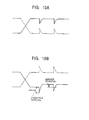
- a time-division switch 101 is formed of a CMOS analog switch formed by connecting an NchMOS transistor and a PchMOS transistor in parallel to each other.
- the time-division switch 101 is connected between a common signal line 102 for transmitting a signal voltage output from a driver IC (not shown) and a signal line 103 of an LCD panel.
- a select pulse S and its inverted pulse XS to the gates of the respective NchMOS transistor and PchMOS transistor, the time-division switch 101 transmits a signal voltage from the driver IC to the signal line 103.
- the writing potential is changed. Then, the signal potential of the non-selected signal line becomes lower, as illustrated in Fig. 13, with respect to a ground potential (0 V). Then, the gate potential of the NchMOS transistor becomes positive with respect to the potential of the signal line, i.e., to the source potential of the NchMOS transistor. This potential relationship satisfies the condition of switching on (conducting) the NchMOS transistor. As a result, the NchMOS transistor is activated.
- an object of the present invention to provide an LCD device that maintains a high image quality by eliminating the generation of insufficient contrast and non-uniformity of the luminance in the horizontal direction caused by the crosstalk of a signal potential from a selected signal line to a non-selected signal line.
- a liquid crystal display device including a first substrate having a display unit on which pixels are formed at intersections of gate lines for a plurality of rows and signal lines for a plurality of columns, the gate lines and the signal lines being arranged in a matrix.
- a vertical drive circuit is mounted on the first substrate so as to drive the gate lines.
- a horizontal drive circuit outputs a time-series signal potential in correspondence with a predetermined number of time-divided portions.
- a time-division switch time-divides the time-series signal potential outputted from the horizontal drive circuit and supplies the divided time-series signal potential to a given signal line among the signal lines.
- a select pulse generating circuit generates a select pulse for activating the time-division switch.
- a low-level potential of the select pulse is set to be lower than a low-level potential of the signal potential outputted from the honzontal drive circuit.
- a second substrate opposes the first substrate with a predetermined gap therebetween in which a liquid crystal layer is encapsulated between the first substrate and the second substrate.
- the potential of the non-selected signal line is reduced. This further decreases the source potential of an NchMOS transistor of a CMOS transistor, which is used as the time-division switch.
- the low-level potential of the select pulses to be applied to the gate of the NchMOS transistor is lower than the low-level potential of the signal potential. Accordingly, the source potential of the NchMOS transistor does not become lower than the gate potential, which would otherwise activate the NchMOS transistor and cause the charge to flow out of the non-selected signal line via the NchMOS transistor. As a consequence, the potential of the non-selected signal line can be maintained at the initially written potential.
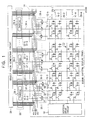
- an LCD panel (display unit) 14 is formed in the following manner.
- n number of column signal lines 12-1 through 12-n formed of, for example, aluminum (A1) are arranged in a matrix on a transparent insulating substrate, for example, a glass substrate (not shown).
- m ( n unit pixels 13 are formed.
- Each unit pixel 13 is formed of, as shown in Fig. 2, a TFT (pixel transistor) 15, made of, for example, polysilicon (Poly-Si) generated by laser recrystallization, a storage capacitor 16, and a liquid crystal capacitor 17.
- the TFTs 15 are connected at gate electrodes thereof to the gate lines 11-1 through 11-m and at source electrodes thereof to the signal lines 12-1 through 12-n.
- the liquid crystal capacitor 17 generates a capacitance between a pixel electrode made of, for example, indium tin oxide (ITO), connected to the TFT 15, and an opposing electrode made of, for example, ITO, facing the pixel electrode, via a liquid crystal material, such as a twisted nematic (TN) liquid crystal.
- ITO indium tin oxide
- TN twisted nematic
- the optical transmittance ratio of the liquid crystal is changed, and the storage capacitor 16 is charged. Accordingly, even if the TFT 15 is turned off, the transmittance ratio of the liquid crystal is maintained due to the charging voltage of the storage capacitor 16 until the TFT 15 is subsequently switched on. According to this technique. the quality of a display image on the LCD panel 14 is improved.
- a vertical drive circuit 18 made of, for example, a polysilicon TFT, is integrally formed on the same substrate on which the LCD panel 14 is formed.
- the vertical dnve circuit 18 selects the unit pixels 13 line-by-line by sequentially supplying a scanning pulse to the gate lines 11-1 through 11-m, each line being connected at one end to an output terminal of the vertical drive circuit 18, thereby performing vertical scanning.
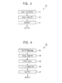
- the vertical drive circuit 18 is formed of, as illustrated in Fig. 3, a shift register 19, a level shifter 20, and a buffer 21.
- a horizontal drive circuit 22 for supplying signal potentials to the signal lines 12-l through 12-n in accordance with image data is formed as an external circuit on a circuit board different from the substrate on which the LCD panel 14 is formed. This will be discussed in greater detail later. Assuming that digital signals are inputted into the horizontal drive circuit 22, it is necessary to convert digital signals into analog signals for driving the liquid crystal.
- the horizontal drive circuit 22 is formed of, as illustrated in Fig. 4, a shift register 23, a level shifter 24, a data latch 25, a digital-to-analog (D/A) converter 26, and a buffer 27.
- Digital image data enabling, for example, at least 8-level 256-color display, is inputted into the horizontal drive circuit 22.
- the n number of column signal lines 12-1 through 12-n are divided by using the number of time-divided portions (in this embodiment, three) as a unit (block).
- the honzontal drive circuit 22 has k number of tape automated bonding (TAB) driver ICs 28-1 through 28-k (hereinafter referred to as the "TAB IC(1) 28-1 through TAB IC(k) 28-k”) corresponding to the number of units k of the signal lines 12-1 through 12-n.
- TAB tape automated bonding
- the TAB IC(1) 28-1 through TAB IC(k) 28-k are mounted on an external circuit board (not shown) different from the substrate on which the LCD panel 14 is formed.
- the TAB IC(1) 28-1 through TAB IC(k) 28-k sequentially output signal potentials to the plurality of signal lines of the individual units in time senes.
- the signal potentials are outputted by inverting the polarity of the image data in every 1H period for the common voltage VCOM.
- k number of time-division switches 30-1 through 30-k are provided for the input stages of the signal lines 12-1 through 12-n.
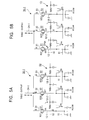
- the time-division switch 30-1 is formed of, as shown in Fig. 2, three CMOS analog switches (transmission switches) 31, 32, and 33, each being formed by connecting a PchMOS transistor and an NchMOS transistor in parallel to each other.
- the time-division switch 30-1 is formed of a TFT made of, for example, polysilicon, and is integrally formed with the LCD panel 14 on the same substrate.
- the other time-division switches 30-2 through 30-k are configured similarly to the time-division switch 30-1.
- the input terminals of the three analog switches 31, 32, and 33 are connected to each other, and the common node is connected to the output terminal of the TAB IC(1) 28-1 via a common signal line 34-1.
- the signal potential having an amplitude of, for example, 0 to 5 V, outputted from the TAB IC(1) 28-1 in time series is supplied to the input terminals of the three analog switches 31, 32, and 33 via the common signal line 34-1.
- Each of the output terminals of the analog switches 31, 32, and 33 is connected to one end of each of the three signal lines 12-1, 12-2, and 12-3, respectively.
- a time-series signal potential is supplied from the TAB IC(2) 28-2 to the time-division switch 30-2 via a common signal line 34-2.
- a time-senes signal potential is supplied from the TAB IC(k) 28-k to the time-division switch 30-k via a common signal line 34-k.
- only one common signal line is provided for each TAB IC. In practice, however, a plurality of common signal lines are provided for a plurality of output pins of each TAB IC.
- control lines are provided for each analog switch, i.e., a total of six control lines 35-1 through 35-6 are arranged in the direction in which the gate lines 11-1 through 11-m are arranged.
- two control input terminals that is, the gate of the NchMOS transistor and the gate of the PchMOS transistor
- the analog switch 31 are connected to the control lines 35-1 and 35-2, respectively
- two control input terminals of the analog switch 32 are connected to the control lines 35-3 and 35-4, respectively
- two control input terminals of the analog switch 33 are connected to the control lines 35-5 and 35-6, respectively.
- Select pulses S1 through S3 and XS1 through XS3 for respectively selecting the three analog switches 31 through 33 of each of the time-division switches 30-1 through 30-k are supplied to the six control lines 35-1 through 35-6 from a select pulse generating circuit 36.
- the select pulse generating circuit 36 is separately formed on an external circuit board different from the substrate on which the LCD panel 14 is formed.
- the select pulses XS1 through XS3 are obtained by inverting the select pulses S1 through S3, respectively.
- the select pulses S1 through S3 and XS1 through XS3 sequentially activate the analog switches 31 through 33 of each of the time-division switches 30-1 through 30-k.
- the select pulses S1 through S3 and XS1 through XS3 are inputted into the LCD panel 14 from the vicinity of the horizontal drive circuit 22, i.e., via a plurality of portions from the upper side of the LCD panel 14. More specifically, six control lines 37-1 through 37-k are respectively laid from the select pulse generating circuit 36 to the six control lines 35-1 through 35-6 located on the LCD panel 14 in correspondence with each of the time-division switches 30-1 through 30-k via an external circuit board (not shown) on which the TAB IC(1) 28-1 through TAB IC(k) 28-k are mounted.
- the wiring of the control lines 35-1 through 35-6 is performed by using, for example, TAB low-expansion tape.
- the control lines 35-1 through 35-6 transmit the select pulses S1, XS1, S2, XS2, S3, and XS3, respectively.
- the low-level signal potential outputted from the TAB IC(1) 28-1 through TAB IC(k) 28-k is set to be 0 V (ground potential).
- the select pulses S1 through S3 and XS1 through XS3 the low-level potential outputted from the select pulse generating circuit 36 is set to be lower than the ground potential, while the high-level potential from the select pulse generating circuit 36 is set to be higher than that (in this embodiment, 5 V) of the signal potential. That is, the select pulse generating circuit 36 generates the pulses having an amplitude of, for example, -2 to 9 V.
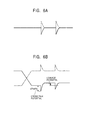
- the signal line 12-1 is not selected and is almost in the floating state. Then, the signal potential of the signal line 12-2 is transferred to the gate line 11 and the Cs line 29, both of which are horizontally arranged, and is further transferred to the non-selected signal line 12-1 via the gate line 11 and the Cs line 29.
- the crosstalk caused by the transfer of the signal potential acts upon an increase in the amplitude potential of the Cs line 29 and the non-selected signal line 12-1.
- the swing of the Cs line 29 and the potential of the non-selected signal line 12-1 caused by the crosstalk are indicated by the waveform diagrams of Figs. 6A and 6B, respectively.
- the waveform diagrams reveal that the crosstalk potential (Vspike transferred onto the Cs line 29 changes the potential of the non-selected signal line 12-1 to be lower than the ground potential (0 V) by about 1.78 V. This is based on simulation results.
- the signal charge stored in the signal line 12-1 flows out to the common signal line 34-1 via the activated NchTFT, thereby lowering the signal potential of the signal line 12-1 from the originally written signal potential. This reduces the pixel potential, resulting in degradation of the image quality in a TN liquid crystal used in this embodiment.
- the low-level potential of the select pulses S1 through S3 and XS1 through XS3 is set to be, for example, -2 V, as shown in Fig. 7. Accordingly, even if the potential of the non-selected signal line 12-1, i.e., the source potential of the NchTFT, fluctuates, as shown in Fig. 8, to the negative side and becomes lower than the ground potential by about 1.78 V owing to the crosstalk potential ( ⁇ Vspike transferred onto the Cs line 29, it does not become lower than the gate potential of the NchTFT, i.e., it is not less than -2 V.
- the gate-source voltage Vgs of the NchTFT does not exceed the threshold value Vth while being maintained in the negative state, which would otherwise activate the NchTFT and cause the signal charge to flow out of the signal line 12-1 to the common signal line 34-1 via the NchTFT.
- the potential of the non-selected signal line 12-1 is maintained at the originally written signal potential.
- Fig. 9 illustrates the relationship between the leakage voltage (leakage of the signal potential) and the threshold voltage Vth of the NchTFT.
- Fig. 9 shows that the threshold voltage Vth can be used in a higher voltage range compared to the range of the threshold voltage Vth used when the low-level potential is set to be the ground potential. Even if the threshold voltage Vth of the NchTFT is reduced due to the process, the leakage voltage can be sufficiently suppressed. As a result, the high image quality can be maintained without being influenced by variations in the characteristics of the transistor.
- the leakage potential of the signal potential is less than 50 mV, as shown in Fig. 9. Such a small level of leakage potential can be ignored with almost no degradation in the image quality.
- the low-level potential of the select pulses S1 through S3 and XS1 through XS3 is set to be lower than the ground potential, assuming that the low-level potential of the signal potential supplied from the TAB IC(1) 28-1 through TAB IC(k) 28-k is 0 V (ground potential). If it is possible to increase the low-level potential of the signal potential to the positive side, for example, to 2 V, the low-level potential of the select pulses S1 through S3 and XS1 through XS3 can be set to be the ground potential.
- the high-level potential of the select pulses S1 through S3 and XS1 through XS3 is set to be, for example, 9 V, assuming that the high-level potential of the signal potential is 5 V.
- the high-level potential of the select pulses S1 through S3 and XS1 through XS3 is set to be higher than the high-level potential of the signal potential, the leakage potential of the PchTFTs of the analog switches 31, 32, and 33 can be suppressed.
- the 1H inversion drive method is employed in which the polarity of the image data to be supplied to each pixel is inverted in every 1H period for the common voltage VCOM.
- the above-described technique can also be applied apply to the 1H common (VCOM) inversion drive method in which the common voltage VCOM is AC-inverted in every 1H period.
- VCOM 1H common inversion drive method
- the potential of the Cs line shown in Fig. 10A and the signal potential of a non-selected signal line shown in Fig. 10B are inverted in every 1H period.
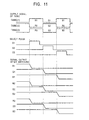
- the signal potentials for the three pixels are sequentially outputted in time series from the TAB IC(1) 28-1 through the TAB IC(3) 28-3 and are transmitted to the time-division switches 30-1, 30-2, and 30-3 via the common signal lines 34-1, 34-2, and 34-3, respectively.
- the timing chart of Fig. 11 reveals that the signal potentials of the individual pixels R1, G1, and B1 are transmitted from the TAB IC(1) 28-1 to the time-division switch 30-1, the signal potentials of the individual pixels R2, G2, and B2 are transmitted from the TAB IC(2) 28-2 to the time-division switch 30-2, and the signal potentials of the individual pixels R3, G3, and B3 are transmitted from the TAB IC(3) 28-3 to the time-division switch 30-3.
- the select pulses through S3 and XS1 through XS3 in synchronization with the above-described time-series signal potentials are also supplied to the time-division switches 30-1 through 30-3
- the analog switch 31 when the select pulse S1 is at a high level, the analog switch 31 is turned on, thereby supplying the signal potentials of the pixels R1 and R3 to the corresponding signal lines among the signal lines 12-1 through 12-n.
- the analog switch 32 When the select pulse S2 is at a high level, the analog switch 32 is activated, thereby supplying the signal potential of the pixel G2 to the corresponding signal line among the signal lines 12-1 through 12-n.
- the analog switch 33 When the select pulse S3 is at a high level, the analog switch 33 is turned on, thereby supplying the signal potentials of the pixels B1 and B3 to the corresponding signal lines among the signal lines 12-1 through 12-n.
- the horizontal drive circuit 22 for driving the signal lines 12-1 through 12-n is placed at one side (upper side in this embodiment) of the LCD panel 14.
- the honzontal drive circuit 22 may be divided into two portions with respect to the common voltage VCOM, and the divided portions may be placed at the upper and lower sides of the LCD panel 14.
- the present invention offers the following advantages.
- the low-level potential of the select pulses for activating the time-division switches is set to be lower than the low-level potential of the signal potential outputted from the horizontal drive circuit. Accordingly, even with the occurrence of the crosstalk of a signal potential from a selected signal line to a non-selected signal line, the charge can be prevented from flowing out of the non-selected signal line via the time-division switch. Thus, the potential of the non-selected signal line can be maintained at the initially written signal potential.
Landscapes
- Engineering & Computer Science (AREA)
- Chemical & Material Sciences (AREA)
- Crystallography & Structural Chemistry (AREA)
- Physics & Mathematics (AREA)
- Computer Hardware Design (AREA)
- General Physics & Mathematics (AREA)
- Theoretical Computer Science (AREA)
- Liquid Crystal Display Device Control (AREA)
- Liquid Crystal (AREA)
- Control Of Indicators Other Than Cathode Ray Tubes (AREA)
Applications Claiming Priority (2)
| Application Number | Priority Date | Filing Date | Title |
|---|---|---|---|
| JP10244773A JP2000075841A (ja) | 1998-08-31 | 1998-08-31 | 液晶表示装置 |
| JP24477398 | 1998-08-31 |
Publications (1)
| Publication Number | Publication Date |
|---|---|
| EP0984424A1 true EP0984424A1 (en) | 2000-03-08 |
Family
ID=17123708
Family Applications (1)
| Application Number | Title | Priority Date | Filing Date |
|---|---|---|---|
| EP99402162A Ceased EP0984424A1 (en) | 1998-08-31 | 1999-08-31 | Liquid crystal display device |
Country Status (3)
| Country | Link |
|---|---|
| US (1) | US6795050B1 (enExample) |
| EP (1) | EP0984424A1 (enExample) |
| JP (1) | JP2000075841A (enExample) |
Cited By (2)
| Publication number | Priority date | Publication date | Assignee | Title |
|---|---|---|---|---|
| FR2801750A1 (fr) * | 1999-11-30 | 2001-06-01 | Thomson Lcd | Procede de compensation des perturbations dues au demultiplexage d'un signal analogique dans un afficheur matriciel |
| CN116256911A (zh) * | 2021-12-09 | 2023-06-13 | 虹彩光电股份有限公司 | 胆固醇液晶显示器装置及改善胆固醇液晶显示器装置画质不均的驱动方法 |
Families Citing this family (16)
| Publication number | Priority date | Publication date | Assignee | Title |
|---|---|---|---|---|
| TW461180B (en) * | 1998-12-21 | 2001-10-21 | Sony Corp | Digital/analog converter circuit, level shift circuit, shift register utilizing level shift circuit, sampling latch circuit, latch circuit and liquid crystal display device incorporating the same |
| JP2001312255A (ja) * | 2000-05-01 | 2001-11-09 | Toshiba Corp | 表示装置 |
| JP2001325798A (ja) * | 2000-05-16 | 2001-11-22 | Sony Corp | 論理回路およびこれを用いた表示装置 |
| JP4183222B2 (ja) * | 2000-06-02 | 2008-11-19 | 日本電気株式会社 | 携帯電話機の省電力駆動方法 |
| US7633472B2 (en) * | 2002-09-23 | 2009-12-15 | Chi Mei Optoelectronics Corporation | Active matrix display devices |
| JP3685176B2 (ja) | 2002-11-21 | 2005-08-17 | セイコーエプソン株式会社 | 駆動回路、電気光学装置及び駆動方法 |
| JP4572316B2 (ja) * | 2003-05-30 | 2010-11-04 | セイコーエプソン株式会社 | 電気光学パネルの駆動回路及び方法、電気光学装置並びに電子機器 |
| JP2005215037A (ja) * | 2004-01-27 | 2005-08-11 | Seiko Epson Corp | 電気光学装置および電子機器 |
| JP4667904B2 (ja) * | 2005-02-22 | 2011-04-13 | 株式会社 日立ディスプレイズ | 表示装置 |
| US7656381B2 (en) * | 2006-01-11 | 2010-02-02 | Tpo Displays Corp. | Systems for providing dual resolution control of display panels |
| US7683878B2 (en) * | 2006-01-23 | 2010-03-23 | Tpo Displays Corp. | Systems for providing dual resolution control of display panels |
| JP4702114B2 (ja) * | 2006-03-08 | 2011-06-15 | エプソンイメージングデバイス株式会社 | デマルチプレクサ、電気光学装置および電子機器 |
| US8300037B2 (en) | 2007-08-02 | 2012-10-30 | Sharp Kabushiki Kaisha | Liquid crystal display device and method and circuit for driving the same |
| JP5285934B2 (ja) * | 2008-03-11 | 2013-09-11 | 株式会社ジャパンディスプレイ | 液晶表示装置 |
| JP4845154B2 (ja) * | 2009-04-02 | 2011-12-28 | ルネサスエレクトロニクス株式会社 | 液晶表示駆動装置および表示システム |
| JP6354355B2 (ja) * | 2014-06-09 | 2018-07-11 | セイコーエプソン株式会社 | 電気光学装置、電子機器、及び電気光学装置の制御方法 |
Citations (2)
| Publication number | Priority date | Publication date | Assignee | Title |
|---|---|---|---|---|
| EP0837446A1 (en) * | 1996-10-18 | 1998-04-22 | Canon Kabushiki Kaisha | Matrix substrate with column driver for use in liquid crystal display |
| US5784042A (en) * | 1991-03-19 | 1998-07-21 | Hitachi, Ltd. | Liquid crystal display device and method for driving the same |
Family Cites Families (9)
| Publication number | Priority date | Publication date | Assignee | Title |
|---|---|---|---|---|
| EP0237809B1 (en) * | 1986-02-17 | 1993-10-06 | Canon Kabushiki Kaisha | Driving apparatus |
| JP2767858B2 (ja) * | 1989-02-09 | 1998-06-18 | ソニー株式会社 | 液晶ディスプレイ装置 |
| JP3173200B2 (ja) * | 1992-12-25 | 2001-06-04 | ソニー株式会社 | アクティブマトリクス型液晶表示装置 |
| CA2112733C (en) * | 1993-01-07 | 1999-03-30 | Naoto Nakamura | Electron beam-generating apparatus, image-forming apparatus, and driving methods thereof |
| KR950007126B1 (ko) * | 1993-05-07 | 1995-06-30 | 삼성전자주식회사 | 액정 디스플레이 구동장치 |
| JPH08171363A (ja) * | 1994-10-19 | 1996-07-02 | Sony Corp | 表示装置 |
| JPH08286642A (ja) * | 1995-04-11 | 1996-11-01 | Sony Corp | 表示装置 |
| JPH1068931A (ja) * | 1996-08-28 | 1998-03-10 | Sharp Corp | アクティブマトリクス型液晶表示装置 |
| JPH1173164A (ja) * | 1997-08-29 | 1999-03-16 | Sony Corp | 液晶表示装置の駆動回路 |
-
1998
- 1998-08-31 JP JP10244773A patent/JP2000075841A/ja active Pending
-
1999
- 1999-08-26 US US09/383,923 patent/US6795050B1/en not_active Expired - Lifetime
- 1999-08-31 EP EP99402162A patent/EP0984424A1/en not_active Ceased
Patent Citations (2)
| Publication number | Priority date | Publication date | Assignee | Title |
|---|---|---|---|---|
| US5784042A (en) * | 1991-03-19 | 1998-07-21 | Hitachi, Ltd. | Liquid crystal display device and method for driving the same |
| EP0837446A1 (en) * | 1996-10-18 | 1998-04-22 | Canon Kabushiki Kaisha | Matrix substrate with column driver for use in liquid crystal display |
Non-Patent Citations (1)
| Title |
|---|
| NISHIHARA Y ET AL: "FULLY INTEGRATED POLY-SI TFT CMOS DRIVERS FOR SELF-SCANNED LIGHT VALVE", SID INTERNATIONAL SYMPOSIUM DIGEST OF PAPERS,US,PLAYA DEL REY, SID, VOL. VOL. 23, PAGE(S) 609-612, ISSN: 0097-966X, XP000479096 * |
Cited By (5)
| Publication number | Priority date | Publication date | Assignee | Title |
|---|---|---|---|---|
| FR2801750A1 (fr) * | 1999-11-30 | 2001-06-01 | Thomson Lcd | Procede de compensation des perturbations dues au demultiplexage d'un signal analogique dans un afficheur matriciel |
| WO2001041112A3 (fr) * | 1999-11-30 | 2001-12-27 | Thomson Lcd | Procede de compensation des perturbations dues au demultiplexage d'un signal analogique dans un afficheur matriciel |
| US6977638B1 (en) | 1999-11-30 | 2005-12-20 | Thales Avionics Lcd S.A. | Method for compensating perturbations caused by demultiplexing an analog signal in a matrix display |
| KR100744988B1 (ko) * | 1999-11-30 | 2007-08-02 | 딸르 아비오닉스 엘씨디 에스.에이. | 매트릭스 디스플레이에서 아날로그 신호를 디멀티플렉싱하는 것에 의하여 유발되는 교란을 보상하는 방법 |
| CN116256911A (zh) * | 2021-12-09 | 2023-06-13 | 虹彩光电股份有限公司 | 胆固醇液晶显示器装置及改善胆固醇液晶显示器装置画质不均的驱动方法 |
Also Published As
| Publication number | Publication date |
|---|---|
| US6795050B1 (en) | 2004-09-21 |
| JP2000075841A (ja) | 2000-03-14 |
Similar Documents
| Publication | Publication Date | Title |
|---|---|---|
| KR100378556B1 (ko) | 액정 표시 장치 | |
| JP4835667B2 (ja) | 液晶表示装置 | |
| KR100927932B1 (ko) | 전기 광학 장치, 구동 회로 및 전자기기 | |
| KR0154832B1 (ko) | 액정 표시 장치 | |
| EP0984424A1 (en) | Liquid crystal display device | |
| US6961042B2 (en) | Liquid crystal display | |
| US6424328B1 (en) | Liquid-crystal display apparatus | |
| US6456267B1 (en) | Liquid crystal display | |
| KR101037554B1 (ko) | 액티브 매트릭스 디스플레이 장치 및 그의 구동 방법 | |
| KR100324912B1 (ko) | 평면표시장치 | |
| CN101154366A (zh) | 用于驱动显示设备的方法和显示设备 | |
| US5745090A (en) | Wiring structure and driving method for storage capacitors in a thin film transistor liquid crystal display device | |
| KR20050039017A (ko) | 액정표시장치 및 그 구동방법 | |
| US6911962B1 (en) | Driving method of active matrix display device | |
| CN1326109C (zh) | 液晶电光器件 | |
| US6091392A (en) | Passive matrix LCD with drive circuits at both ends of the scan electrode applying equal amplitude voltage waveforms simultaneously to each end | |
| JPH08137443A (ja) | 画像表示装置 | |
| US20100066719A1 (en) | Liquid crystal display device, its driving circuit and driving method | |
| JP2000275611A (ja) | 液晶表示装置 | |
| KR100412120B1 (ko) | 액정표시장치의 구동회로 및 그 구동방법 | |
| JP2005024979A (ja) | 表示装置及びその駆動方法 | |
| US6219018B1 (en) | Active matrix type display device | |
| JP2007293369A (ja) | 液晶表示装置 | |
| JP4283172B2 (ja) | 液晶電気光学装置 | |
| KR101177577B1 (ko) | 액정표시장치 |
Legal Events
| Date | Code | Title | Description |
|---|---|---|---|
| PUAI | Public reference made under article 153(3) epc to a published international application that has entered the european phase |
Free format text: ORIGINAL CODE: 0009012 |
|
| AK | Designated contracting states |
Kind code of ref document: A1 Designated state(s): DE GB NL |
|
| AX | Request for extension of the european patent |
Free format text: AL;LT;LV;MK;RO;SI |
|
| 17P | Request for examination filed |
Effective date: 20000906 |
|
| AKX | Designation fees paid |
Free format text: DE GB NL |
|
| 17Q | First examination report despatched |
Effective date: 20061229 |
|
| STAA | Information on the status of an ep patent application or granted ep patent |
Free format text: STATUS: THE APPLICATION HAS BEEN REFUSED |
|
| 18R | Application refused |
Effective date: 20110415 |