EP0984360B1 - Bus signal line driver - Google Patents
Bus signal line driver Download PDFInfo
- Publication number
- EP0984360B1 EP0984360B1 EP99202783A EP99202783A EP0984360B1 EP 0984360 B1 EP0984360 B1 EP 0984360B1 EP 99202783 A EP99202783 A EP 99202783A EP 99202783 A EP99202783 A EP 99202783A EP 0984360 B1 EP0984360 B1 EP 0984360B1
- Authority
- EP
- European Patent Office
- Prior art keywords
- mentioned
- level
- signal
- terminal
- switching means
- Prior art date
- Legal status (The legal status is an assumption and is not a legal conclusion. Google has not performed a legal analysis and makes no representation as to the accuracy of the status listed.)
- Expired - Lifetime
Links
Images

Classifications
-
- G—PHYSICS
- G06—COMPUTING OR CALCULATING; COUNTING
- G06F—ELECTRIC DIGITAL DATA PROCESSING
- G06F13/00—Interconnection of, or transfer of information or other signals between, memories, input/output devices or central processing units
- G06F13/38—Information transfer, e.g. on bus
- G06F13/40—Bus structure
- G06F13/4063—Device-to-bus coupling
- G06F13/4068—Electrical coupling
- G06F13/4072—Drivers or receivers
- G06F13/4077—Precharging or discharging
-
- Y—GENERAL TAGGING OF NEW TECHNOLOGICAL DEVELOPMENTS; GENERAL TAGGING OF CROSS-SECTIONAL TECHNOLOGIES SPANNING OVER SEVERAL SECTIONS OF THE IPC; TECHNICAL SUBJECTS COVERED BY FORMER USPC CROSS-REFERENCE ART COLLECTIONS [XRACs] AND DIGESTS
- Y02—TECHNOLOGIES OR APPLICATIONS FOR MITIGATION OR ADAPTATION AGAINST CLIMATE CHANGE
- Y02D—CLIMATE CHANGE MITIGATION TECHNOLOGIES IN INFORMATION AND COMMUNICATION TECHNOLOGIES [ICT], I.E. INFORMATION AND COMMUNICATION TECHNOLOGIES AIMING AT THE REDUCTION OF THEIR OWN ENERGY USE
- Y02D10/00—Energy efficient computing, e.g. low power processors, power management or thermal management
Definitions
- the present invention relates to a signal line driver for the transmission and output of a binary signal such as a digital signal.
- Driver circuits which set a driven line to a preferred value when a signal is not bing transmitted are known in general, such as your example the arrangement in United States Patent US 4,651,036.
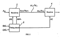
- FIG. 1 a circuit diagram of a bus driver according to Application Example 1 of the present invention is shown.
- This bus driver for example, is provided within an address buffer of a semiconductor memory device, and transmits a one bit address signal by means of a differential system.
- this bus driver 2 is connected to a receiver, for example, a receiver 4 for an address decoder, via the pair of complementary bus lines AL, AL_.
- the bus driver 2 has a one bit address signal (AIN) input and in response to the logical value of this input address signal (AIN), outputs a complementary pair of address signals (AOUT, AOUT_) having the logic H level and L level on the transmit end of the bus lines AL, AL_.
- the receiver 4 receives the address signals (Ain, Ain_) which are equivalent to the address signals (AOUT, AOUT_) respectively from the bus driver 2 at the input side of the bus lines AL, AL_.
- the timing circuit 6 supplies the later explained timing signals (PRC, AEN_), and (KC), which will be explained below and are used to control the bus driver 2 and the receiver 4.
- the NMOS transistors 10,12 used as switching transistors for the drivers are each connected between the transmit ends for both bus lines AL, AL_ respectively and a terminal at the power supply voltage (V ss ) (for example, 0 volts) for the reference L level.
- V ss power supply voltage
- a switching control circuit 14 that controls the switching of NMOS transistor 10 ON-OFF is constructed of a PMOS transistor 16, an NMOS transistor 18, an inverter 20, 22, a NAND gate 24, and a NOR gate 26.
- the source terminal of the PMOS transistor 16 is connected to the power supply terminal of the power supply voltage (V DD ) (for example, 3.3 volts) for the reference H level, and the source terminal of the NMOS transistor 18 is connected to a terminal at the power supply voltage (V SS ).
- V DD power supply voltage
- V SS power supply voltage
- the transmit end of the bus line AL is connected to the gate terminal of the PMOS transistor, and the precharge control signal input terminal 28 is connected to the gate terminal of the NMOS transistor 18.
- the drain terminal (node (Nc)) of the PMOS transistor 16 and the NMOS transistor 18 is connected to the input terminal of the inverter 20.
- the output terminal of the inverter 20 is connected to one of the input terminals of the NAND gate 24.
- the capacitor C1 is connected between the input terminal of the inverter 20 and a terminal at the power supply voltage (V SS ).
- the pulse signal input terminal 30 is connected to the input terminal of the inverter 22, and the output terminal of the inverter 22 is connected to the other input terminal of the NAND gate 24.
- the output terminal of the NAND gate 24 is connected to one of the input terminals of the NOR gate 26.
- the address enable input signal terminal 32 is connected to the other input terminal of the NOR gate 26.
- the output terminal of the NOR gate 26 is connected to the gate terminal of the NMOS transistor 10.
- a switching control circuit 34 that controls the switching of NMOS transistor 12 ON-OFF is constructed of a PMOS transistor 36, an NMOS transistor 38, an inverter 40, a NAND gate 42, and a NOR gate 44.
- the source terminal of the PMOS transistor 36 is connected to a terminal at the power supply voltage (V DD ), and the source terminal of the NMOS transistor 38 is connected to a terminal at the power supply voltage (V SS ).
- the sending terminal of bus-line AL_ is connected to the gate terminal of PMOS transistor 36, and pre-charge control signal input terminal 28 is connected to the gate terminal of NMOS transistor 38.
- the drain terminal (node (Nd)) of the PMOS transistor 36 and the NMOS transistor 38 are connected to the input terminal of the inverter 40. Also, the capacitor C2 is connected between the input terminal of the inverter 40 and a terminal at the power supply voltage (V SS ). The output terminal of the inverter 40 is connected to one of the input terminals of the NAND gate 42. The address signal input terminal 30 is connected to the other input terminal of the NAND gate 42.
- the output terminal of the NAND gate 42 is connected to one of the input terminals of the NOR gate 44.
- the address enable signal input terminal 32 is connected to the other output terminal of the NOR gate 44.
- the output terminal of the NOR gate 44 is connected to the gate terminal of the NMOS transistor 12.
- the PMOS transistors 46, 48 used as switching elements for the bias and the precharging are each connected between the transmission ends for both bus lines AL, AL_ respectively and a terminal at the power supply voltage (V DD ).
- the output terminal of the inverter 50 is connected to the gate terminal of these PMOS transistors 46, 48.
- the precharge control signal input terminal 28 is connected to the input terminal of the inverter 50.
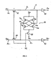
- FIG. 3 A circuit diagram for the receiver 4 is shown in FIG. 3.
- This receiver 4 has transfer gates 52, 54 that are connected between the receive ends of the bus lines (AL, AL_) and the internal lines (JL, JL_), and a binary comparator differential amplifier 56 that is connected to the internal lines (JL, JL_).
- the drive timing signal (KC) from the timing circuit 6 is activated at the H level, at the same time that the transfer gates 52, 54 that are made up of PMOS transistors are switched OFF and are electrically blocked from the bus lines AL, AL_, the switch 58 made up of an NMOS transistor is switched ON and the differential amplifier 56 is switched on.
- the differential amplifier 56 When the differential amplifier 56 is switched on, it detects the differential of the receive address signals (Ain, Ain_) on the internal lines (JL, JL_),and amplifies the differential so that it equals the difference between the H level and the L level of the power supply voltages (V DD ) and (V SS ).
- the receive address signals (Ain, Ain_) that are amplified in this manner to the reference H level (V DD ) and the reference L level (V SS ) by means of the differential amplifier 56 are sent to a signal receiving section (not illustrated) of a later stage via the inverters 60, 62, respectively.
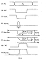
- the precharge control signal (PRC) from the timing circuit 6 that is applied to the input terminal 28 is active (H level). Due to this, the output of the inverter 50 is at the L level, and the PMOS transistors 46, 48 that are the switching elements used for the precharge are each switched ON.
- the address enable signal (AEN) from the timing circuit 6 that is applied to the input terminal 32 is inactive (H level). Due to this, the outputs of both NOR gates 26, 44 are at the L level, and both NMOS transistors 10, 12 that are the switching elements used to drive remain OFF.
- the bus lines AL, AL_ are precharged by the power supply voltage (V DD ) via the respective transistors 46, 48 that are switched ON, and held at the voltage level of (V DD ).
- the precharge control signal (PRC) is at the H level
- the respective NMOS transistors 18, 38 are switched ON, the respective nodes (Nc, Nd) are driven to the voltage of the power supply voltage (V SS ), in other words, the L level, and the output of both inverters 20, 40 become the H level, respectively.
- the precharge control signal (PRC) becomes the L level
- the output of the inverter 50 becomes the H level
- the PMOS transistors 46, 48 used for the precharge are turned OFF.
- the NMOS transistors 18, 38 within the switching control circuits 14, 34 are turned OFF.
- the respective nodes (Nc, Nd) due to the operation of the capacitors C1, C2, are held at the potential of (V SS ) (L level), and the output of both inverters 20, 40 are held at the H level.
- the bus line AL_ is connected to a terminal at the power supply voltage (V SS ) through the NMOS transistor 12 which is switched ON, the electrical charge on the bus line AL_ is discharged, and as shown in FIG. 4(E), the potential of the bus line AL_ drops rapidly.
- the PMOS transistor 36 is turned on, and the node (Nd) becomes the voltage level of (V DD ).
- the voltage level (V DD ) at node (Nd) is maintained with the aid of capacitor C2. Due to this, the output of the inverter 40 becomes an L level - the output of the NAND gate 42 [becomes] the H level, the output (GS_) of the NOR gate 44 drops to the L level, and the NMOS transistor 12 returns to the OFF state.
- the bus line AL_ stops discharging, and over the entire bus line AL_, the potential between the transmit end (near end) and the receive end (far end), in particular, is equalized. Due to this, at the near end (AOUT_), as shown in FIG. 4(E), the potential rises more than the minimum point (Vc). On the other hand, at the far end (Ain_), as shown in FIG. 4(F), the potential drops further. Also, both potentials are stabilized by the averaging voltage level (VF) until they are equivalent.
- VF averaging voltage level
- this average voltage level (VF) is a level that is lower than the threshold value (VTH) for the binary detection amplification in the receiver 4 of the receive end.
- the voltage level (VF) or the amplitude (V DD - VF) for the logic L level in the transmit address signal can be adjusted arbitrarily by means of controlling the period (Tc), in other words, the switching state of the NMOS transistor 10,12 so that the output (GS), (GS_) of the NOR gate 26, 44 goes to the H level in the pulse condition. Specifically, for example, this can be adjusted arbitrarily by changing the size of the NMOS transistor 10, 12.
- this period (Tc) by setting this period (Tc) to a value that is sufficiently smaller than the pulse time period that is regulated by the address enable signal (AEN_) or the precharge control signal (PRC), the voltage (VF) for the L level in the transmit address signal (AOUT, AOUT_) (Ain, Ain_) is made higher than the power supply voltage (V SS ), the amplitude (V DD -VF) of the transmit address signal is made smaller than the full amplitude (V DD -V SS ), and can be the necessary minimum magnitude.
- the power that is consumed in this bus driver 2 is mainly a factor of the operating (discharge) current when the NMOS transistors 10, 12 used for the driver are turned on.
- the period (Tc) is short, and the amplitude (V DD -VF) for the transmit address signal (AOUT, AOUT_) is small, the power consumption is greatly reduced.
- the access speed can be increased.
- the switching element used for the precharge is constructed by the PMOS transistors 46, 48, and the timing between the precharge control signal (PRC) and the address enable signal (AEN_) is adjusted (FIG. 4(B), (C)) so that these PMOS transistors 46, 48 and the NMOS transistors 10, 12 used for driving are not turned ON at the same time.
- PRC precharge control signal
- AEN_ address enable signal
- the switching elements used for the precharge can be interchanged with resistive elements used for the bias.
- both transistors 46, 48 can be used as resistive elements.
- the above-mentioned application example is a construction wherein the driving switching elements (NMOS transistors 10, 12) are connected between the transmission end of the bus lines (AL, AL_) and terminals at the power supply voltage (V SS ) at the L level.
- the driving switching elements NMOS transistors 10, 12
- the driving switching elements are connected between the transmission end of the bus lines (AL, AL_) and the terminals at the power supply voltage (V DD ) at the H level.
- switching elements and resistive elements used for the precharge and the bias are connected between the transmission end of the bus lines (AL, AL_) and a terminal at the power supply voltage (V SS ) at the L level.
- the circuit construction (FIG. 3) for the receiver 4 is only one example for the above-mentioned application example, and other receiver circuits can be used.
- the above-mentioned application examples are devices related to a bus driver for the purpose of transmitting an address signal.
- the present invention is also applicable to drives such as control buses or data buses, and is applicable to signal lines driven for the purpose of transmitting arbitrary digital signals or binary signals.
- the above-mentioned capacitors C1, C2 can be constructed using parasitic capacitance.
- the signal line driver of the present invention since this design drives a signal line at the minimum necessary amplitude in order to transmit a binary signal, the power consumption can be reduced and the transmission delay time can be shortened.
Landscapes
- Engineering & Computer Science (AREA)
- General Engineering & Computer Science (AREA)
- Theoretical Computer Science (AREA)
- Computer Hardware Design (AREA)
- Physics & Mathematics (AREA)
- General Physics & Mathematics (AREA)
- Logic Circuits (AREA)
- Dram (AREA)
- Static Random-Access Memory (AREA)
- Dc Digital Transmission (AREA)
Applications Claiming Priority (2)
| Application Number | Priority Date | Filing Date | Title |
|---|---|---|---|
| JP26088498A JP4198792B2 (ja) | 1998-08-31 | 1998-08-31 | 信号線駆動回路 |
| JP26088498 | 1998-08-31 |
Publications (3)
| Publication Number | Publication Date |
|---|---|
| EP0984360A2 EP0984360A2 (en) | 2000-03-08 |
| EP0984360A3 EP0984360A3 (en) | 2004-03-17 |
| EP0984360B1 true EP0984360B1 (en) | 2007-03-21 |
Family
ID=17354098
Family Applications (1)
| Application Number | Title | Priority Date | Filing Date |
|---|---|---|---|
| EP99202783A Expired - Lifetime EP0984360B1 (en) | 1998-08-31 | 1999-08-26 | Bus signal line driver |
Country Status (4)
| Country | Link |
|---|---|
| US (1) | US6300799B1 (enExample) |
| EP (1) | EP0984360B1 (enExample) |
| JP (1) | JP4198792B2 (enExample) |
| DE (1) | DE69935559T2 (enExample) |
Families Citing this family (8)
| Publication number | Priority date | Publication date | Assignee | Title |
|---|---|---|---|---|
| EP1334593A2 (en) | 2000-11-13 | 2003-08-13 | Primarion, Inc. | Method and circuit for pre-emphasis equalization in high speed data communications |
| US7026847B2 (en) * | 2003-12-31 | 2006-04-11 | Altera Corporation | Programmable current booster for faster edge-rate output in high speed applications |
| US20060244478A1 (en) * | 2005-04-29 | 2006-11-02 | Kent Smith | Systems and methods for reducing signal ringing |
| KR100881195B1 (ko) * | 2007-05-22 | 2009-02-05 | 삼성전자주식회사 | 고주파 성능을 개선한 odt 회로 |
| JP5776418B2 (ja) * | 2011-07-29 | 2015-09-09 | 富士通セミコンダクター株式会社 | 半導体記憶装置及び半導体記憶装置の制御方法 |
| US9065544B2 (en) * | 2012-09-28 | 2015-06-23 | Osram Sylvania Inc. | Pulse-based binary communication |
| CN112953496B (zh) * | 2021-02-04 | 2022-04-22 | 电子科技大学 | 一种高速动态比较器 |
| CN120825152B (zh) * | 2025-09-17 | 2025-12-09 | 成都芯正微电子科技有限公司 | 一种能够自关断的边沿加速电路 |
Family Cites Families (10)
| Publication number | Priority date | Publication date | Assignee | Title |
|---|---|---|---|---|
| FR2560410B1 (fr) * | 1984-02-24 | 1986-06-06 | Efcis | Circuit de precharge de bus de transfert de donnees logiques |
| US5134316A (en) * | 1990-12-12 | 1992-07-28 | Vlsi Technology, Inc. | Precharged buffer with reduced output voltage swing |
| US5214320A (en) * | 1992-06-12 | 1993-05-25 | Smos Systems, Inc. | System and method for reducing ground bounce in integrated circuit output buffers |
| KR960006911B1 (ko) * | 1992-12-31 | 1996-05-25 | 현대전자산업주식회사 | 데이타 출력버퍼 |
| US5453705A (en) * | 1993-12-21 | 1995-09-26 | International Business Machines Corporation | Reduced power VLSI chip and driver circuit |
| KR0146169B1 (ko) * | 1995-06-30 | 1998-12-01 | 김주용 | 포스트 차지 로직에 의한 펄스 전달 장치 |
| US5760620A (en) * | 1996-04-22 | 1998-06-02 | Quantum Effect Design, Inc. | CMOS limited-voltage-swing clock driver for reduced power driving high-frequency clocks |
| KR0179930B1 (ko) * | 1996-07-12 | 1999-04-01 | 문정환 | 출력 버퍼 제어 회로 |
| US6054874A (en) * | 1997-07-02 | 2000-04-25 | Cypress Semiconductor Corp. | Output driver circuit with switched current source |
| US6130556A (en) * | 1998-06-16 | 2000-10-10 | Lsi Logic Corporation | Integrated circuit I/O buffer with 5V well and passive gate voltage |
-
1998
- 1998-08-31 JP JP26088498A patent/JP4198792B2/ja not_active Expired - Fee Related
-
1999
- 1999-08-26 EP EP99202783A patent/EP0984360B1/en not_active Expired - Lifetime
- 1999-08-26 DE DE69935559T patent/DE69935559T2/de not_active Expired - Lifetime
- 1999-08-30 US US09/385,344 patent/US6300799B1/en not_active Expired - Lifetime
Also Published As
| Publication number | Publication date |
|---|---|
| US6300799B1 (en) | 2001-10-09 |
| DE69935559D1 (de) | 2007-05-03 |
| EP0984360A3 (en) | 2004-03-17 |
| JP4198792B2 (ja) | 2008-12-17 |
| DE69935559T2 (de) | 2007-12-06 |
| JP2000076868A (ja) | 2000-03-14 |
| EP0984360A2 (en) | 2000-03-08 |
Similar Documents
| Publication | Publication Date | Title |
|---|---|---|
| EP0746820B1 (en) | Circuit for Coupling Data Communication Busses | |
| EP0788059B1 (en) | Driver circuit device | |
| JP3238826B2 (ja) | 出力回路 | |
| US12009943B2 (en) | Field bus driver circuit | |
| US5808487A (en) | Multi-directional small signal transceiver/repeater | |
| US5793226A (en) | Data output buffer for multiple power supplies | |
| EP0984360B1 (en) | Bus signal line driver | |
| EP0887935A1 (en) | Noise isolation circuit | |
| US6687166B1 (en) | Bus interface circuit and receiver circuit | |
| EP0660963B1 (en) | High speed memory sense amplifier with noise reduction | |
| US20040032776A1 (en) | Semiconductor memory device comprising circuit for precharging data line | |
| US5739701A (en) | Input/output buffer circuit having reduced power consumption | |
| US6037827A (en) | Noise isolation circuit | |
| EP1043728B1 (en) | Semiconductor memory device | |
| US5834949A (en) | Bus driver failure detection system | |
| US6081138A (en) | High-speed sense amplifier | |
| US5933028A (en) | Data transmitter circuit and semiconductor device using the same | |
| EP0352965A2 (en) | Data transmission system | |
| US6236234B1 (en) | High-speed low-power consumption interface circuit | |
| US6157219A (en) | Amplifier for a semiconductor device and a method of controlling the same | |
| KR100363040B1 (ko) | 저소비 전력을 가지는 반도체 기억 장치 | |
| US6087887A (en) | Signal routing circuits having selective high impedance and low impedance output states | |
| US5430391A (en) | Data input/output control circuit | |
| KR100713907B1 (ko) | 반도체 장치의 라인 구동 회로 | |
| US5751654A (en) | Driver device for selection lines for a multiplexer, to be used in a wide range of supply voltages, particularly for non-volatile memories |
Legal Events
| Date | Code | Title | Description |
|---|---|---|---|
| PUAI | Public reference made under article 153(3) epc to a published international application that has entered the european phase |
Free format text: ORIGINAL CODE: 0009012 |
|
| AK | Designated contracting states |
Kind code of ref document: A2 Designated state(s): AT BE CH CY DE DK ES FI FR GB GR IE IT LI LU MC NL PT SE |
|
| AX | Request for extension of the european patent |
Free format text: AL;LT;LV;MK;RO;SI |
|
| PUAL | Search report despatched |
Free format text: ORIGINAL CODE: 0009013 |
|
| AK | Designated contracting states |
Kind code of ref document: A3 Designated state(s): AT BE CH CY DE DK ES FI FR GB GR IE IT LI LU MC NL PT SE |
|
| AX | Request for extension of the european patent |
Extension state: AL LT LV MK RO SI |
|
| RIC1 | Information provided on ipc code assigned before grant |
Ipc: 7G 11C 8/06 B Ipc: 7H 03F 3/30 B Ipc: 7G 06F 13/40 A |
|
| 17P | Request for examination filed |
Effective date: 20040917 |
|
| AKX | Designation fees paid |
Designated state(s): DE FR GB |
|
| 17Q | First examination report despatched |
Effective date: 20050405 |
|
| GRAP | Despatch of communication of intention to grant a patent |
Free format text: ORIGINAL CODE: EPIDOSNIGR1 |
|
| GRAS | Grant fee paid |
Free format text: ORIGINAL CODE: EPIDOSNIGR3 |
|
| GRAA | (expected) grant |
Free format text: ORIGINAL CODE: 0009210 |
|
| AK | Designated contracting states |
Kind code of ref document: B1 Designated state(s): DE FR GB |
|
| REG | Reference to a national code |
Ref country code: GB Ref legal event code: FG4D |
|
| REF | Corresponds to: |
Ref document number: 69935559 Country of ref document: DE Date of ref document: 20070503 Kind code of ref document: P |
|
| ET | Fr: translation filed | ||
| PLBE | No opposition filed within time limit |
Free format text: ORIGINAL CODE: 0009261 |
|
| STAA | Information on the status of an ep patent application or granted ep patent |
Free format text: STATUS: NO OPPOSITION FILED WITHIN TIME LIMIT |
|
| 26N | No opposition filed |
Effective date: 20071227 |
|
| PGFP | Annual fee paid to national office [announced via postgrant information from national office to epo] |
Ref country code: DE Payment date: 20140901 Year of fee payment: 16 |
|
| PGFP | Annual fee paid to national office [announced via postgrant information from national office to epo] |
Ref country code: FR Payment date: 20140725 Year of fee payment: 16 Ref country code: GB Payment date: 20140725 Year of fee payment: 16 |
|
| REG | Reference to a national code |
Ref country code: DE Ref legal event code: R119 Ref document number: 69935559 Country of ref document: DE |
|
| GBPC | Gb: european patent ceased through non-payment of renewal fee |
Effective date: 20150826 |
|
| REG | Reference to a national code |
Ref country code: FR Ref legal event code: ST Effective date: 20160429 |
|
| PG25 | Lapsed in a contracting state [announced via postgrant information from national office to epo] |
Ref country code: GB Free format text: LAPSE BECAUSE OF NON-PAYMENT OF DUE FEES Effective date: 20150826 Ref country code: DE Free format text: LAPSE BECAUSE OF NON-PAYMENT OF DUE FEES Effective date: 20160301 |
|
| PG25 | Lapsed in a contracting state [announced via postgrant information from national office to epo] |
Ref country code: FR Free format text: LAPSE BECAUSE OF NON-PAYMENT OF DUE FEES Effective date: 20150831 |