EP0981063A2 - Polarisator, OPTISCHES ELEMENT UND OPTISCHER KOPF - Google Patents
Polarisator, OPTISCHES ELEMENT UND OPTISCHER KOPF Download PDFInfo
- Publication number
- EP0981063A2 EP0981063A2 EP99203376A EP99203376A EP0981063A2 EP 0981063 A2 EP0981063 A2 EP 0981063A2 EP 99203376 A EP99203376 A EP 99203376A EP 99203376 A EP99203376 A EP 99203376A EP 0981063 A2 EP0981063 A2 EP 0981063A2
- Authority
- EP
- European Patent Office
- Prior art keywords
- optical
- light
- optical element
- light beam
- light receiving
- Prior art date
- Legal status (The legal status is an assumption and is not a legal conclusion. Google has not performed a legal analysis and makes no representation as to the accuracy of the status listed.)
- Withdrawn
Links
- 230000003287 optical effect Effects 0.000 title claims abstract description 442
- 239000011347 resin Substances 0.000 claims description 51
- 229920005989 resin Polymers 0.000 claims description 51
- 239000000758 substrate Substances 0.000 claims description 47
- 239000004065 semiconductor Substances 0.000 claims description 40
- 239000000463 material Substances 0.000 claims description 32
- 239000000853 adhesive Substances 0.000 claims description 14
- 230000001070 adhesive effect Effects 0.000 claims description 14
- 230000008859 change Effects 0.000 claims description 12
- 238000001746 injection moulding Methods 0.000 claims description 12
- 239000011521 glass Substances 0.000 claims description 10
- 230000001788 irregular Effects 0.000 claims description 2
- 230000010287 polarization Effects 0.000 description 59
- 239000010409 thin film Substances 0.000 description 46
- 238000000034 method Methods 0.000 description 40
- 238000001704 evaporation Methods 0.000 description 24
- 230000008020 evaporation Effects 0.000 description 22
- 239000010408 film Substances 0.000 description 21
- 238000001514 detection method Methods 0.000 description 20
- 238000004519 manufacturing process Methods 0.000 description 17
- 230000008569 process Effects 0.000 description 17
- 230000005540 biological transmission Effects 0.000 description 14
- 239000010410 layer Substances 0.000 description 14
- 230000008033 biological extinction Effects 0.000 description 13
- 239000012780 transparent material Substances 0.000 description 13
- XUIMIQQOPSSXEZ-UHFFFAOYSA-N Silicon Chemical compound [Si] XUIMIQQOPSSXEZ-UHFFFAOYSA-N 0.000 description 11
- 238000010586 diagram Methods 0.000 description 11
- 229910052710 silicon Inorganic materials 0.000 description 11
- 239000010703 silicon Substances 0.000 description 11
- 239000011248 coating agent Substances 0.000 description 10
- 238000000576 coating method Methods 0.000 description 10
- 229920003229 poly(methyl methacrylate) Polymers 0.000 description 10
- 239000004926 polymethyl methacrylate Substances 0.000 description 10
- 230000035882 stress Effects 0.000 description 10
- 201000009310 astigmatism Diseases 0.000 description 7
- 238000000137 annealing Methods 0.000 description 6
- 238000006243 chemical reaction Methods 0.000 description 6
- 238000000465 moulding Methods 0.000 description 6
- 238000012545 processing Methods 0.000 description 6
- 238000005452 bending Methods 0.000 description 5
- 238000000151 deposition Methods 0.000 description 5
- 230000001747 exhibiting effect Effects 0.000 description 5
- 230000002093 peripheral effect Effects 0.000 description 5
- 239000002985 plastic film Substances 0.000 description 5
- 239000004417 polycarbonate Substances 0.000 description 5
- 230000009467 reduction Effects 0.000 description 5
- 230000032683 aging Effects 0.000 description 4
- 230000004075 alteration Effects 0.000 description 4
- 230000008901 benefit Effects 0.000 description 4
- 239000006059 cover glass Substances 0.000 description 4
- 238000005530 etching Methods 0.000 description 4
- 230000006872 improvement Effects 0.000 description 4
- 238000003754 machining Methods 0.000 description 4
- 229910052751 metal Inorganic materials 0.000 description 4
- 239000002184 metal Substances 0.000 description 4
- 229920006255 plastic film Polymers 0.000 description 4
- 230000015556 catabolic process Effects 0.000 description 3
- 238000005520 cutting process Methods 0.000 description 3
- 238000006731 degradation reaction Methods 0.000 description 3
- 239000003989 dielectric material Substances 0.000 description 3
- 230000010354 integration Effects 0.000 description 3
- 239000007788 liquid Substances 0.000 description 3
- 238000001259 photo etching Methods 0.000 description 3
- BQCADISMDOOEFD-UHFFFAOYSA-N Silver Chemical compound [Ag] BQCADISMDOOEFD-UHFFFAOYSA-N 0.000 description 2
- 239000005083 Zinc sulfide Substances 0.000 description 2
- 238000010521 absorption reaction Methods 0.000 description 2
- 239000002131 composite material Substances 0.000 description 2
- 238000010276 construction Methods 0.000 description 2
- 238000012937 correction Methods 0.000 description 2
- 238000005336 cracking Methods 0.000 description 2
- 238000013461 design Methods 0.000 description 2
- 239000003822 epoxy resin Substances 0.000 description 2
- 239000004973 liquid crystal related substance Substances 0.000 description 2
- 229910001635 magnesium fluoride Inorganic materials 0.000 description 2
- 239000005304 optical glass Substances 0.000 description 2
- 229920003023 plastic Polymers 0.000 description 2
- 239000004033 plastic Substances 0.000 description 2
- 229920000515 polycarbonate Polymers 0.000 description 2
- 229920000647 polyepoxide Polymers 0.000 description 2
- 229920000098 polyolefin Polymers 0.000 description 2
- 238000003825 pressing Methods 0.000 description 2
- 229910052709 silver Inorganic materials 0.000 description 2
- 239000004332 silver Substances 0.000 description 2
- 238000005549 size reduction Methods 0.000 description 2
- 238000012546 transfer Methods 0.000 description 2
- 229910052984 zinc sulfide Inorganic materials 0.000 description 2
- ZCYVEMRRCGMTRW-UHFFFAOYSA-N 7553-56-2 Chemical compound [I] ZCYVEMRRCGMTRW-UHFFFAOYSA-N 0.000 description 1
- 235000007173 Abies balsamea Nutrition 0.000 description 1
- 239000004925 Acrylic resin Substances 0.000 description 1
- 229920000178 Acrylic resin Polymers 0.000 description 1
- 239000004857 Balsam Substances 0.000 description 1
- 244000018716 Impatiens biflora Species 0.000 description 1
- 239000004793 Polystyrene Substances 0.000 description 1
- NIXOWILDQLNWCW-UHFFFAOYSA-N acrylic acid group Chemical group C(C=C)(=O)O NIXOWILDQLNWCW-UHFFFAOYSA-N 0.000 description 1
- 239000012790 adhesive layer Substances 0.000 description 1
- 230000006399 behavior Effects 0.000 description 1
- 238000005219 brazing Methods 0.000 description 1
- 239000000919 ceramic Substances 0.000 description 1
- 230000023077 detection of light stimulus Effects 0.000 description 1
- 238000005516 engineering process Methods 0.000 description 1
- 238000002474 experimental method Methods 0.000 description 1
- 210000000887 face Anatomy 0.000 description 1
- 239000012530 fluid Substances 0.000 description 1
- PCHJSUWPFVWCPO-UHFFFAOYSA-N gold Chemical compound [Au] PCHJSUWPFVWCPO-UHFFFAOYSA-N 0.000 description 1
- 239000010931 gold Substances 0.000 description 1
- 229910052737 gold Inorganic materials 0.000 description 1
- 238000005469 granulation Methods 0.000 description 1
- 230000003179 granulation Effects 0.000 description 1
- 238000010438 heat treatment Methods 0.000 description 1
- 229910052740 iodine Inorganic materials 0.000 description 1
- 239000011630 iodine Substances 0.000 description 1
- 150000002500 ions Chemical class 0.000 description 1
- ORUIBWPALBXDOA-UHFFFAOYSA-L magnesium fluoride Chemical compound [F-].[F-].[Mg+2] ORUIBWPALBXDOA-UHFFFAOYSA-L 0.000 description 1
- 230000000873 masking effect Effects 0.000 description 1
- 238000002844 melting Methods 0.000 description 1
- 239000000203 mixture Substances 0.000 description 1
- 230000004048 modification Effects 0.000 description 1
- 238000012986 modification Methods 0.000 description 1
- 239000003973 paint Substances 0.000 description 1
- 239000002245 particle Substances 0.000 description 1
- 239000012994 photoredox catalyst Substances 0.000 description 1
- 229920002223 polystyrene Polymers 0.000 description 1
- 210000001747 pupil Anatomy 0.000 description 1
- 238000005096 rolling process Methods 0.000 description 1
- 238000007789 sealing Methods 0.000 description 1
- 229920002545 silicone oil Polymers 0.000 description 1
- 238000004088 simulation Methods 0.000 description 1
- 239000007779 soft material Substances 0.000 description 1
- 239000000126 substance Substances 0.000 description 1
- 229920001187 thermosetting polymer Polymers 0.000 description 1
- 238000002834 transmittance Methods 0.000 description 1
- 238000009281 ultraviolet germicidal irradiation Methods 0.000 description 1
- 238000007738 vacuum evaporation Methods 0.000 description 1
- 208000016261 weight loss Diseases 0.000 description 1
- DRDVZXDWVBGGMH-UHFFFAOYSA-N zinc;sulfide Chemical compound [S-2].[Zn+2] DRDVZXDWVBGGMH-UHFFFAOYSA-N 0.000 description 1
Images


Classifications
-
- G—PHYSICS
- G11—INFORMATION STORAGE
- G11B—INFORMATION STORAGE BASED ON RELATIVE MOVEMENT BETWEEN RECORD CARRIER AND TRANSDUCER
- G11B7/00—Recording or reproducing by optical means, e.g. recording using a thermal beam of optical radiation by modifying optical properties or the physical structure, reproducing using an optical beam at lower power by sensing optical properties; Record carriers therefor
- G11B7/12—Heads, e.g. forming of the optical beam spot or modulation of the optical beam
- G11B7/135—Means for guiding the beam from the source to the record carrier or from the record carrier to the detector
- G11B7/1353—Diffractive elements, e.g. holograms or gratings
-
- G—PHYSICS
- G02—OPTICS
- G02B—OPTICAL ELEMENTS, SYSTEMS OR APPARATUS
- G02B5/00—Optical elements other than lenses
- G02B5/30—Polarising elements
- G02B5/3025—Polarisers, i.e. arrangements capable of producing a definite output polarisation state from an unpolarised input state
-
- G—PHYSICS
- G11—INFORMATION STORAGE
- G11B—INFORMATION STORAGE BASED ON RELATIVE MOVEMENT BETWEEN RECORD CARRIER AND TRANSDUCER
- G11B7/00—Recording or reproducing by optical means, e.g. recording using a thermal beam of optical radiation by modifying optical properties or the physical structure, reproducing using an optical beam at lower power by sensing optical properties; Record carriers therefor
- G11B7/12—Heads, e.g. forming of the optical beam spot or modulation of the optical beam
- G11B7/123—Integrated head arrangements, e.g. with source and detectors mounted on the same substrate
-
- G—PHYSICS
- G11—INFORMATION STORAGE
- G11B—INFORMATION STORAGE BASED ON RELATIVE MOVEMENT BETWEEN RECORD CARRIER AND TRANSDUCER
- G11B7/00—Recording or reproducing by optical means, e.g. recording using a thermal beam of optical radiation by modifying optical properties or the physical structure, reproducing using an optical beam at lower power by sensing optical properties; Record carriers therefor
- G11B7/12—Heads, e.g. forming of the optical beam spot or modulation of the optical beam
- G11B7/13—Optical detectors therefor
- G11B7/131—Arrangement of detectors in a multiple array
-
- G—PHYSICS
- G11—INFORMATION STORAGE
- G11B—INFORMATION STORAGE BASED ON RELATIVE MOVEMENT BETWEEN RECORD CARRIER AND TRANSDUCER
- G11B7/00—Recording or reproducing by optical means, e.g. recording using a thermal beam of optical radiation by modifying optical properties or the physical structure, reproducing using an optical beam at lower power by sensing optical properties; Record carriers therefor
- G11B7/12—Heads, e.g. forming of the optical beam spot or modulation of the optical beam
- G11B7/135—Means for guiding the beam from the source to the record carrier or from the record carrier to the detector
- G11B7/1356—Double or multiple prisms, i.e. having two or more prisms in cooperation
-
- G—PHYSICS
- G11—INFORMATION STORAGE
- G11B—INFORMATION STORAGE BASED ON RELATIVE MOVEMENT BETWEEN RECORD CARRIER AND TRANSDUCER
- G11B7/00—Recording or reproducing by optical means, e.g. recording using a thermal beam of optical radiation by modifying optical properties or the physical structure, reproducing using an optical beam at lower power by sensing optical properties; Record carriers therefor
- G11B7/12—Heads, e.g. forming of the optical beam spot or modulation of the optical beam
- G11B7/135—Means for guiding the beam from the source to the record carrier or from the record carrier to the detector
- G11B7/1365—Separate or integrated refractive elements, e.g. wave plates
- G11B7/1367—Stepped phase plates
-
- G—PHYSICS
- G11—INFORMATION STORAGE
- G11B—INFORMATION STORAGE BASED ON RELATIVE MOVEMENT BETWEEN RECORD CARRIER AND TRANSDUCER
- G11B11/00—Recording on or reproducing from the same record carrier wherein for these two operations the methods are covered by different main groups of groups G11B3/00 - G11B7/00 or by different subgroups of group G11B9/00; Record carriers therefor
- G11B11/10—Recording on or reproducing from the same record carrier wherein for these two operations the methods are covered by different main groups of groups G11B3/00 - G11B7/00 or by different subgroups of group G11B9/00; Record carriers therefor using recording by magnetic means or other means for magnetisation or demagnetisation of a record carrier, e.g. light induced spin magnetisation; Demagnetisation by thermal or stress means in the presence or not of an orienting magnetic field
- G11B11/105—Recording on or reproducing from the same record carrier wherein for these two operations the methods are covered by different main groups of groups G11B3/00 - G11B7/00 or by different subgroups of group G11B9/00; Record carriers therefor using recording by magnetic means or other means for magnetisation or demagnetisation of a record carrier, e.g. light induced spin magnetisation; Demagnetisation by thermal or stress means in the presence or not of an orienting magnetic field using a beam of light or a magnetic field for recording by change of magnetisation and a beam of light for reproducing, i.e. magneto-optical, e.g. light-induced thermomagnetic recording, spin magnetisation recording, Kerr or Faraday effect reproducing
- G11B11/10532—Heads
- G11B11/10541—Heads for reproducing
- G11B11/10543—Heads for reproducing using optical beam of radiation
-
- G—PHYSICS
- G11—INFORMATION STORAGE
- G11B—INFORMATION STORAGE BASED ON RELATIVE MOVEMENT BETWEEN RECORD CARRIER AND TRANSDUCER
- G11B7/00—Recording or reproducing by optical means, e.g. recording using a thermal beam of optical radiation by modifying optical properties or the physical structure, reproducing using an optical beam at lower power by sensing optical properties; Record carriers therefor
- G11B7/12—Heads, e.g. forming of the optical beam spot or modulation of the optical beam
- G11B7/135—Means for guiding the beam from the source to the record carrier or from the record carrier to the detector
- G11B7/1372—Lenses
- G11B2007/13727—Compound lenses, i.e. two or more lenses co-operating to perform a function, e.g. compound objective lens including a solid immersion lens, positive and negative lenses either bonded together or with adjustable spacing
Definitions
- the present invention relates to a polarizer, an optical element, and a small sized optical head constructed with these polarizer and optical element.
- the optical head in accordance with the present invention has a configuration suitable for use in particular in recording and reproduction of information on a magneto-optical recording medium.
- a conventional polarizer such as a polarizing beam splitter is produced by depositing a polarizing optical thin film on triangular prisms of glass by means of vacuum evaporation and further by bonding these triangular prisms to each other.
- Conventional optical heads for recording and reproducing of information on a magneto-optical recording medium are realized with a polarizing beam splitter as disclosed for example in U. S. Patent No. 4,764,912, or with a dichroic polarizing plate as disclosed for example in U. S. Patent No. 4,933,924, or otherwise with a birefringent prism such as a Wollaston prism.
- the optical parts used in these techniques are of bulk type which are produced from optical glass by means of cutting and lapping.
- the present invention provides a polarizer, an optical element, and an optical head as will be described in the following paragraphs.
- FIGS 1-53 relate to embodiments in accordance with the present invention, wherein:
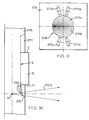
- Figure la is a plan view of a polarizer in accordance with a first embodiment of the present invention
- Figure lb is a cross-sectional view thereof.
- the polarizer has a plurality of edge lines 201 and it has a sawtooth-shaped section as shown in Figure lb.
- the polarizer is formed by means of evaporation to deposit a polarizing optical thin film 203 on a transparent substrate 202 made of a plastic sheet with edge lines 201 and by further coating a transparent material 204 such as a transparent resin.
- the edge lines are arranged at an angle of 45° to the sides of the polarizer so that the transmitted light beam 206 is polarized at 45° relative to the sides of the polarizer.
- the polarization direction may be an arbitrary value by arranging the edge lines in a desired direction.
- the space between the edge lines may be any values less than twice the thickness of the transparent substrate 202.
- a preferable material for the transparent substrate 202 is a resin exhibiting transparency for a wavelength of the light to be used, such as an acrylic resin, polycarbonate, amorphous polyolefin, and polystyrene.
- the transparent material 204 is a resin exhibiting transparency for a wavelength of the light to be used, such as an ultraviolet-cured resin, epoxy resin, and balsam. With this filling transparent material 204, the direction of the transmitted light beam 206 becomes the same as that of the incident light beam 205.
- a mold for producing the polarizer may be made by means of machining when the space between the edge lines is rather wide such as larger than several hundred microns, and by means of photo-etching and blazing when the space between the edge lines is rather narrow for example several ten microns to several microns.
- the polarizer produced in such a manner as described above is thin enough and has high transparency. In addition, it shows a large extinction ratio (the ratio of the amount of transmitted light with P-polarization to that of transmitted light with S-polarization). More specifically, it is possible to obtain as high transparency as 98%, and a large extinction ratio such as 500:1.
- this polarizer may be used as an analyzer in an optical head for detecting a magneto-optical signal.
- the polarizer may also be applied to a liquid crystal display, an optical shutter, or the like.
- FIG. 2 is a plan view of a polarizer in accordance with a second embodiment of the present invention.
- This polarizer comprises a first substrate 302 having a plurality of edge lines 301 and a second substrate 304 having a plurality of edge lines 303 formed in a different direction from that of the edge lines 301 in the first substrate, these substrate 302 and 303 being injection-molded into a single piece with a resin such as a PMMA resin, a dielectric multi-layer film acting as a polarizing optical thin film being deposited by evaporation on the saw-tooth shaped surface having the edge lines.
- the polarizer with this configuration may be used in an optical head of a magneto-optic recording device.
- the edge lines 301 are arranged at 45° and the edge lines 303 are arranged at -45°.
- the number of the edge lines may be only one for each substrate. In this case, these substrate have a V-shaped section.
- the first and second substrates are not necessarily needed to be arranged adjacent to each other. There may be a space between these substrates as required for a specific construction and these substrate may be connected to each other. Such a construction may be realized by injection molding with plastic.
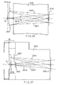
- Figure 11 is a plan view of a polarizer in accordance with a third embodiment of the present invention.
- the vertical and horizontal directions are defined as Y- and X-directions, respectively.
- a substrate 1206 made of a transparent material has regions 1202, 1203, 1204, and 1205 with inclined planes.
- Light beam 1207, 1208, 1209, and 1210 are incident on these regions, respectively.
- the polarization direction of the light is set to 45° with respect to the X-axis as designated by an arrow 1201.
- Figure 12a is a cross-sectional view of the regions 1202 and 1203, taken in the X-direction.
- Figure 12b is a cross-sectional view of the regions 1202 and 1203, taken in the Y-direction.
- both of the regions 1202 and 1203 have an inclined plane arranged in the same direction, that is, the angle of the inclined plane is 45° with respect to the substrate.
- a polarizing optical thin film is deposited by evaporation on the inclined plane 1211 and a transparent material 1212 is filled in the space between the inclined plane and the surface of the substrate.
- these regions 1204 and 1205 have an inclined plane arranged in the direction different by 90° from that of the regions 1202 and 1203, that is to say, in the Y-direction. Both of the regions 1204 and 1205 have an inclined plane in the same direction wherein the angle of these inclined planes is 45° with respect to the substrate.
- a polarizing optical thin film is deposited by evaporation on the inclined plane 1216 and a transparent material 1217 is filled in the space from the inclined plane 1216 up to the surface of the substrate.
- the P-polarization component can pass through the inclined plane 1211 and the S-polarization component is reflected from the inclined plane 1211.
- the light beam 1213 with polarization in the direction 1201 is incident on the regions 1202 and 1203, only its P-polarization component can selectively pass through the inclined plane 1211.
- only the X-direction component 1214 of the light polarized in the direction 1201 can pass through the inclined plane 1211.
- the inclined plane 1216 transmits the P-polarization component and reflects the S-polarization component. Therefore, the inclined planes 1216 transmit only the P-polarization component of the light beam 1218 with polarization in the direction 1201 incident on the regions 1204 and 1205.
- the directions of the inclined planes of these regions 1204 and 1205 are different by 90° from those of the regions 1202 and 1203, thus the only Y-direction component 1219 of the light with polarization in the direction 1201 can pass. In this way, it becomes possible to perform light detection in the directions ⁇ 45° via the regions 1202, 1203 and the regions 1204, 1205, respectively.
- the direction of the light to be detected can be modified from ⁇ 45° into an arbitrary direction by setting the directions of the inclined planes to symmetrical directions such that the absolute values of the angles with respect to the polarization direction are the same.
- the light detection when required in the direction of ⁇ A°, it may be arranged such that with respect to the polarization direction the angle between the normal line to the inclined plane and the plane containing the optical axis is +A° for one inclined plane and -A° for the other inclined plane.
- the angle between the normal line to the inclined plane and the optical axis of light may be set to an arbitrary value as long as the polarizing thin film formed on the inclined plane may transmit the P-polarization component of the light and may reflect the S-polarization component.
- the incidence angle of the light incident on the inclined plane is larger than 20° with respect to the normal line of the inclined plane.
- Figure 14 is a plan view of a polarizer in accordance with a fourth embodiment of the present invention.
- the vertical and horizontal directions are defined as Y- and X-directions, respectively.
- a substrate 1304 made of a transparent material has regions 1302 and 1303.
- Light beams 1305, 1306, and 1307, 1308 are incident on the above mentioned regions, respectively.
- the polarization direction of the light is set to 45° with respect to the X-axis as designated by an arrow 1301.
- Figure 15a is a cross-sectional view of the region 1302, taken in the X-direction.
- Figure 15b is a cross-sectional view of the region 1302, taken in the Y-direction.
- the regions 1202 have an inclined plane arranged in the X-direction, wherein the angle of the inclined plane is set to 45° with respect to the substrate.
- a polarizing thin film is deposited by evaporation on the inclined plane 1309 and a transparent material 1313 is filled in the space from the inclined plane 1216 up to the surface of the substrate.
- the region 1303 has an inclined plane arranged in the direction different by 90° from that of the region 1302, that is to say, it is arranged in the Y-direction.
- the region 1303 has an inclined plane in the Y-direction and the angle of the inclined plane is set to 45° with respect to the substrate.
- a polarizing thin film is deposited by evaporation on the inclined plane 1314 and a transparent material 1318 is filled in the space from the inclined plane 1314 up to the surface of the substrate.
- the inclined plane 1309 transmits the P-polarization component and reflects the S-polarization component.
- the inclined plane 1314 transmits the P-polarization component and reflects the S-polarization component. Therefore, the inclined plane 1314 transmits selectively only the P-polarization component of the light beams 1307 and 1308 with polarization in the direction 1301 incident on the region 1303.
- the direction of the inclined plane of this region 1303 is different by 90° from that of the region 1302, only the Y-direction component 1316 of the light polarized in the direction 1301 can pass. In this way, the region 1302 and the region 1303 can perform light detection in the directions ⁇ 45°, respectively.
- the direction of the light detection can be modified from ⁇ 45° into an arbitrary direction by setting the directions of the inclined planes to symmetrical directions such that the absolute values of the angles with respect to the polarization direction are the same.
- arrangement may be done such that with respect to the polarization direction the angle between the normal line to the inclined plane and the plane containing the optical axis is +A° for one inclined plane and -A° for the other inclined plane.
- the angle between the normal line to the inclined plane and the optical axis of light may be set to an arbitrary value as long as the polarizing thin film formed on the inclined plane may transmit the P-polarization component of the light and may reflect the S-polarization component.
- the incidence angle of the light incident on the inclined plane is larger than 20° with respect to the normal line of the inclined plane.
- Figure 3a is a side view of an optical head in accordance with a fifth embodiment of the present invention and Figure 3b is a plan view thereof.
- Light is emitted from a semiconductor laser 401 acting as a light source, and this light is reflected from a holographic element 402 on which brazing is performed, and the light reaches a magneto-optical recording medium 404 after passing through an objective lens 403.
- the light is reflected from the magneto-optical recording medium 404 and passes again through the objective lens 403.
- the light is diffracted into two directions by the holographic element 402.
- the holographic element 402 has two regions which are separated from each other by a dividing line 407. Each of these regions produces a light beam, and astigmatism is added by the holographic element 402 to each of these light beams in such a manner that polarities of the added astigmatism are opposite to each other.
- the split light beams are detected by a polarizer 405 shown in embodiment 2. Then, photoelectric-conversion is performed on these light beams by a photosensor 406 acting as a light receiving device.
- the structure of the photosensor 406 is shown in Figure 4. There are provided six rectangular light receiving regions 501, 502, 503, 504, 505, and 506, wherein the regions 501 and 503 are interconnected to each other, and the regions 504 and 506 are also interconnected to each other. There are also provides four terminals 507, 508, 509, and 510.
- the polarizer 405 is bonded onto the photosensor 406 via a transparent resin.
- the cross section of the resultant unit is shown in Figure 5. It will be seen that the unit is configured by bonding the polarizer 405 onto the photosensor 406 via the transparent resin 601.
- Figure 6 shows a relationship between the polarization direction 701 of the light source and directions of the edge lines in the first and second substrates.
- 45° is used as the value a. This angle is preferable because this angle provides a maximum modulation amplitude.
- Figure 7 shows vertical angles at the top portion 801 and at the bottom portion 802 of the sawtooth-shaped section.
- 90° is used as the vertical angle. This angle is preferable because it becomes possible to make the unwanted S-polarization component return back to the incident direction. Thus, little stray light is introduced.
- FIG 17 is a side view of an optical head in accordance with a sixth embodiment of the present invention.
- a light beam is emitted from a semiconductor laser 1409 acting as a light source and the light beam is incident on a polarizer 1406 shown in the previous embodiments.
- the light beam passes through a holographic element 1405 which is bonded to the polarizer.
- an objective lens focuses the light beam onto a magneto-optical recording medium 1401.
- the holographic element 1405 is bonded to the polarizer 1406, the spaces between the holographic element and the inclined planes in the regions 1418 and 1419 are filled with a transparent resin. With this arrangement, the accuracy of the surfaces through which the light beam passes is determined effectively only by the accuracy of the surface of the holographic element.
- the light beam focused on the magneto-optical recording medium obtains a magneto-optical signal when it is reflected from the magneto-optical recording medium, and it returns to the objective lens 1402. After passing through the objective lens, the returning light beam is focused along the same path as the optical path 1412 toward the magneto-optical recording medium and incident on the holographic element 1403.
- the light beam is diffracted by the holographic element, and diffraction of ⁇ first order results in light beams 1413 and 1414, respectively.
- the light beam 1413 is incident on the region 1418 of the polarizer and the light beam 1414 is incident on the region 1419 of the polarizer.
- Figure 18 is a plan view of the polarizer 1406.
- the inclined plane of the region 1418 is arranged such that the plane containing the normal line of the inclined plane and the optical axis makes an angle of +45° with respect to the polarization direction 1415 of the light emitted from the semiconductor laser.
- the inclined plane of the region 1419 is arranged such that the plane containing the normal line of the inclined plane and the optical axis makes an angle of -45° with respect to the polarization direction 1415 of the light emitted from the semiconductor laser.
- the same polarizing thin film which transmits a P-polarization component and reflects a S-polarization component is deposited by evaporation on the inclined planes 1418 and 1419.
- the transmission directions associated with the P-polarization and S-polarization are such ones designated by reference numerals 1416 and 1417, respectively, for the corresponding regions 1418 and 1419.
- these regions 1418 and 1419 can detect the components with polarization of ⁇ 45°, respectively, with respect to the polarization direction 1415 of the light emitted from the semiconductor laser.
- the light beam 1413 passing through the region associated with the detection of polarization of +45° is incident on the light receiving device 1410.
- the light beam 1414 passing through the region associated with detection of -45° is incident on the light receiving device 1411.
- the semiconductor laser 1409 and light receiving devices 1410, 1411 are installed in the same package 1408. These devices are housed with the package 1408 and the optical element wherein the optical element consists of the polarizer 1406 and the holographic element 1405 bonded to each other. This arrangement also acts as protection for the semiconductor laser 1409 and the light receiving devices 1410 and 1411 from environment such as humidity. Both of the light receiving devices 1410 and 1411 are formed on the same silicon chip. Both types of edge-emitting and surface-emitting may be used as a semiconductor laser 1409 to obtain the similar optical head.
- FIG 19 is a side view of an optical head in accordance with a seventh embodiment of the present invention.
- a light beam is emitted from a semiconductor laser 1409 acting as a light source.
- the light beam passes through a cover glass 1503 with which a package is sealed, and further passes through a polarizer 1501 which has detector regions 1502 and 1504 on the side facing the semiconductor laser and which has a holographic surface 1505 on the side facing a magneto-optical recording medium.
- the light beam is focused onto the magneto-optical recording medium 1401 by an objective lens 1402.
- the cover glass is bonded to the polarizer 1501
- the spaces between the cover glass and the inclined planes in the regions 1502 and 1504 are filled with a transparent adhesive.
- the light beam focused on the magneto-optical recording medium When the light beam focused on the magneto-optical recording medium is reflected from it, the light beam obtains a magneto-optical signal. Then, the light beam returns to the objective lens 1402. After passing through the objective lens 1402, the returning light beam is focused along the same path as the optical path 1412 toward the magneto-optical recording medium, and incident on the hologram 1505. The light beam is diffracted by the hologram, and diffraction of ⁇ first order results in light beams 1506 and 1507, respectively. The light beam 1506 is incident on the region 1502 of the polarizer and the light beam 1507 is incident on the region 1504 of the polarizer.
- Figure 20 is a plan view of the composite optical device 1501.
- the inclined plane of the region 1502 is arranged such that the plane containing the normal line of the inclined plane and the optical axis makes an angle of +45° with respect to the polarization direction 1415 of the light emitted from the semiconductor laser.
- the inclined plane of the region 1504 is arranged such that the plane containing the normal line of the inclined plane and the optical axis makes an angle of -45° with respect to the polarization direction 1415 of the light emitted from the semiconductor laser.
- the same polarizing thin film which transmits a P-polarization component and reflects a S-polarization component is deposited by evaporation on the inclined planes 1502 and 1504
- the transmission directions associated with the P-polarization and S-polarization are such ones designated by reference numerals 1508 and 1509, respectively, for the corresponding regions 1502 and 1504.
- these regions 1502 and 1504 can detect the components of ⁇ 45° polarization, respectively, with respect to the polarization direction 1415 of the light emitted from the semiconductor laser.
- the light beam 1506 passing through the region associated with detection of polarization of ⁇ 45° is incident on the light receiving device 1410.
- the light beam 1507 passing through the region associated with detection of polarization of -45° is incident on the light receiving device 1411.
- the semiconductor laser 1409 and light receiving devices 1410 and 1411 are installed in the same package 1408. These devices are protected from environment such as humidity by being sealed with the package 1408 and an optical element wherein the optical element comprises the composite optical element 1501 and the cover glass 1503 bonded together.
- FIG 21 is a side view of an optical head in accordance with an eighth embodiment of the present invention.
- a semiconductor laser 1608 is mounted on a silicon substrate 1605.
- Photodiodes 1609 and 1610 are formed on the silicon substrate 1605.
- a light beam emitted from the semiconductor laser 1608 is incident on a substrate 1602 on which a polarizer is formed.
- the light 1412 emitted from the laser passes through a region 1601.
- Figures 23a and 23b illustrating cross sections of the region 1601, taken in the directions parallel to and perpendicular to the polarization direction, respectively, the plane containing the normal line to the inclined plane 1601 and the optical axis coincides with the polarization direction.
- the light beam 1412 is incident on the inclined plane 1601 as a light beam with P-polarization.
- the inclined plane 1601 is coated with a evaporated polarizing thin film so that it transmits the P-polarization component and reflects the S-polarization component.
- the light beam 1412 emitted from the semiconductor laser is polarized in the direction 1415. Therefore, the light beams 1412 can pass through the regions 1601 with almost no loss.
- the holographic element 1405 is bonded to the polarizer 1602, the spaces between the holographic element and the inclined planes in the regions 1601, 1603, and 1604 are filled with a transparent adhesive.
- the light beam 1412 After passing through the holographic element 1405, the light beam 1412 is focused onto the magneto-optical recording medium 1401 by an objective lens 1402. When the light beam focused on the magneto-optical recording medium is reflected from it, the light beam obtains a magneto-optical signal. Then, the light beam returns to the objective lens 1402. After passing through the objective lens 1402, the returning light beam is focused along the same path as the optical path 1412 toward the magneto-optical recording medium, and incident on the hologram 1403. The light beam is diffracted by the hologram, and diffraction of ⁇ first order results in light beams 1606 and 1607, respectively.
- the light beam 1606 is incident on the region 1603 of the polarizer and the light beam 1607 is incident on the region 1604 of the polarizer.
- Figure 22 is a plan view of the polarizer 1602.
- the inclined plane of the region 1603 is arranged such that the plane containing the normal line of the inclined plane and the optical axis makes an angle of -45° with respect to the polarization direction 1415 of the light emitted from the semiconductor laser.
- the inclined plane of the region 1604 is arranged such that the plane containing the normal line of the inclined plane and the optical axis makes an angle of +45° with respect to the polarization direction 1415 of the light emitted from the semiconductor laser.
- the same kind of polarizing thin film which transmits the P-polarization component and reflects the S-polarization component is deposited by evaporation on the inclined planes 1601, 1603, and 1604. Due to the same polarizing thin films deposited on the inclined planes 1601, 1603, and 1604, the regions 1603 and 1604 exhibit the transmission directions associated with the P-polarization designated by reference numerals 1611 and 1612, respectively. Thus, these regions 1603 and 1604 can detect the polarization components of ⁇ 45°, respectively, with respect to the polarization direction 1415 of the light emitted from the semiconductor laser. Besides, the regions 1601 can transmit the amount of almost 100% of light emitted from the semiconductor laser. If this arrangement is adopted, during the evaporation process of the polarizing thin film, it is unnecessary to mask the area on which the light beam emitted from the semiconductor laser is to be incident. Thus, a great cost reduction can be achieved.
- the light beam 1606 passing through the region for detecting polarization of +45° is incident on the light receiving device 1609.
- the light beam 1607 passing through the region for detecting polarization of -45° is incident on the light receiving device 1610.
- the semiconductor laser 1608 and light receiving devices 1609 and 1610 are installed in the same package 1408. These devices are protected from environment such as humidity by being sealed with the package 1408 and the optical element bonded to the polarizer 1602.
- the light receiving devices 1609 and 1610 are formed on the same silicon wafer, on which the semiconductor laser 1608 is mounted so that the light beam emitted from the semiconductor laser 1608 may come out from the silicon wafer in the direction perpendicular to the silicon wafer after reflected from the inclined plane formed in the silicon wafer. If a surface-emitting type semiconductor laser is used, the light beam emitted from the semiconductor laser can come out from the silicon wafer in the direction perpendicular to the silicon wafer without using a reflection element.
- the angle between the incident light and the normal line to the inclined plane covered with a evaporated polarizing thin film may be larger than 45° so as to obtain a polarizer exhibiting a higher extinction ratio.
- the angle between the incident light and the normal line to the inclined plane covered with a evaporated polarizing thin film may be less than 45° so as to obtain a thinner polarizer, which further leads to a thinner optical head.
- Figure 24 is a plan view of a light receiving device in an optical head in accordance with a ninth embodiment of the present invention.
- the optical system in this optical head is configured with the optical system shown in embodiment 8.
- a semiconductor laser 1608 is mounted on a silicon substrate 1605 on which photodiodes 1702, 1703, 1704, 1705, 1706, and 1707 are formed.
- Reference numerals 1708 and 1709 denote the spots on the sensor illuminated with the light beam detected in the direction of +45° with respect to the polarization direction of the semiconductor laser, wherein the detection of light is performed by a polarizer shown in embodiment 5.
- Reference numerals 1710 and 1711 denote the spots on the sensor illuminated with the light beam detected in the direction of +45° with respect to the polarization direction of the semiconductor laser.
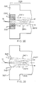
- Figure 25 is a block diagram showing a magneto-optical detection circuit in accordance with this embodiment 9.
- the current signals from the photodiodes 1702, 1703, 1704, 1705, 1706, and 1707 are converted to voltage signals.
- the resultant outputs of current-to-voltage conversion associated with the photodiodes 1702, 1703, and 1704 are added to each other by an adder circuit 1709.
- the resultant outputs of current-to-voltage conversion associated with the photodiodes 1705, 1706, and 1707 are added to each other by an adder circuit 1710.
- a differential circuit 1711 detects the difference between the output of the adder circuit 1709 and the output of the adder circuit 1710 to obtain a magneto-optical signal 1713.
- An adder circuit 1712 adds the output of the adder circuit 1709 and the output of the adder circuit 1710 so as to obtain an ROM signal 1714 such as a pre-pit signal.
- Figure 8 shows an optical head in accordance with a tenth embodiment of the present invention.
- a light beam is emitted from a semiconductor laser 901 and then it passes through a holographic element 902. Then, the light beam reaches the magneto-optical recording medium 904 after passing through a objective lens 903. The light beam is reflected from the magneto-optical recording medium 904 and passes again through the objective lens 903. Then, the light beam is split into two different directions due to the diffraction by the holographic element 902.
- the split light beams pass through polarizers 905 and 906 shown in embodiment 1 and are converted from the optical signals to electric signals by photodiodes 907 and 908.
- preferable directions of the edge lines are +45° and -45° with respect to the polarization direction of the light source.
- Figure 9 is a schematic diagram illustrating a method for producing an optical device in accordance with a eleventh embodiment of the present invention.
- a mold 1003 heated at a high temperature with a heater 1002 is moved in the direction denoted by the arrow 1004 so as to press a sheet 1001 of a transparent substrate made of PMMA with the mold 1003.
- the structure 1005 having a shape of sawtooth is obtained.
- a thin dielectric film is deposited on it by evaporation.
- a glass block may also be used as a transparent substrate. In this case, it is preferable to heat the mold up to a higher temperature than in the case of previous example.
- the mold may be made as follows. A pattern is formed on the mold by means of machining with a grinder or by means of photo-etching. Then, inclined planes are formed by means of blazing. In the production of the mold, it is preferable to use machining when the space between the edge lines is larger than 100 ⁇ m and the photo-etching is preferable when the space is less than 100 ⁇ m.
- FIG 10 is a schematic diagram illustrating another method for producing an optical device in accordance with a twelfth embodiment of the present invention.
- a roller 1102 having a sawtooth-shaped surface is pressed onto a transparent substrate of a plastic film 1101 and the roller 1102 is rotated on the plastic film 1101 so as to transfer the sawtooth structure to the film 1101.
- the roller may be heated as required.
- a multi-layer dielectric thin film acting as a polarizing optical thin film is formed by evaporation on the plastic film 1101.
- the plastic film is cut into a polarizer.
- the roller may be made by directly machining a metal cylinder so as to form a saw-toothed structure on its surface, or otherwise, after forming a saw-toothed structure on the surface of a flat plate, the roller may be obtained by wrapping the flat plate around a cylinder.
- Figure 26 is a schematic diagram illustrating a method for producing an optical device by plastic injection molding in accordance with a thirteenth embodiment of the present invention.
- metal molds 1801 and 1802 are prepared which define the shape of a polarizer having inclined planes.
- a melted resin is injected with a pressure through a gate 1803 into the molds.
- the molds 1801 and 1802 are removed.
- the gate portion is cut off.
- the structure of a polarizer in accordance with the present invention is obtained.
- a multi-layer dielectric thin film acting as a polarizing optical thin film is deposited by evaporation on the surface 1804 having the inclined planes. Furthermore, the spaces adjacent to the inclined planes are filled with a transparent resin having a refractive index approximately the same as that of the injected resin. In this way, a complete polarizer in accordance with the present invention can-be obtained.
- glass may also by used as a material to be injected into the molds to obtain a similar structure.
- Figure 27 is a side view of an optical head in accordance with a fourteenth embodiment of the present invention
- Figure 28 is a side view of a pick-up configured with this optical head.
- reference numeral 10 denotes a light emitting device consisting of a semiconductor laser acting as a light source of the optical head.
- Reference numeral 2120 denotes an optical element called a cover plate.
- Reference numerals 2130 and 2170 denote a hologram comprising a curved diffraction grating, and a light receiving device consisting of a multi-divided photodiode, respectively.
- Reference numeral 80 denotes a package for containing and holding the light emitting device 10 and the light receiving device 2170.
- the package 80 consists of a case having an aperture on one side and this aperture is covered and sealed with the optical element 2120. All these elements are combined into one body to form an optical head 1 in accordance with this embodiment.
- a light source and an optical system for detection are formed into the shape of a cubic body as small as about 5 ⁇ 5 ⁇ 5 mm 3 and different functions are also combined as will be described later in more detail.
- reference numeral 2 denotes a case of the optical pick-up within which the optical head 1 described above is contained.
- a mirror 40, and an objective lens 50 are also contained in the case 2 so that the whole elements are driven in an integral fashion (in operation of servo-focusing and servo-tracking and the like).
- the objective lens 50 is only one lens included in the pick-up, thus achieving an optical system with a finite compact configuration. More specifically, the distance between the object and the image (total track) of the objective lens 50 is as small as about 15 mm. As a result, the size and weight reductions of the case 2 are achieved. With this embodiment, it is possible to obtain an optical pick-up having a light weight such as 2 g as a whole.
- Reference numeral 60 denotes a optical recording medium or optical disk which has grooved tracks (not shown) with a small pitch on its recording surface.
- the optical element 2120 called a cover plate has a step L formed on the surface near the light emitting device 10, thus dividing the surface area into a flat area 2121 and a stepped area 2122.
- This optical element 2120 may be easily made by injection-molding of an optical resin such as PMMA (poly methyl methacrylate), PC (polycarbonate), and APO (amorphous polyolefin), or otherwise, it may be made by pressing low-melting glass at a high temperature.
- PMMA poly methyl methacrylate
- PC polycarbonate
- APO amorphous polyolefin
- a recess 2171 and a inclined plane 2172 at nearly the central portion of the light receiving device 2170 and the light emitting device 10 is mounted in the recess 2171 in the horizontal position so that the light beam 2100 emitted via the light emitting face 11 is reflected from the inclined plane 2172 thus providing a divergent light beam 2101a emerging in the direction perpendicular to the surface of the light receiving device 2170, as shown in Figure 29 or 30.
- the inclined plane 2172 is inclined approximately at 45°.
- the recess 2171 and the inclined plane 2172 may be rather readily formed in the light receiving device 2170 made of a silicon substrate by anisotropic etching. Gold thin film may be deposited by evaporation on the inclined plane 2172 so as to obtain a reflecting plane exhibiting a high reflection factor.
- the virtual light emitting point which is the mirror image of the real light emitting point of the light emitting device 10 about the inclined plane 2172 formed in the light receiving device 2170 lies at the position apart downward (to the left in Figure 30) from the light receiving surface of the light receiving device 2170, as shown in Figure 30.
- the technology of the surface-emitting semiconductor laser has not been established well yet. Thus, it is impossible to produce both of a light emitting device and a light receiving device on the same chip in a full monolithic fashion by using successive fabrication processes.
- the virtual light emitting point 15 exists at a location apart downward from the light receiving device 2170 by for example 0.08 mm.
- a stem (a rectangular metal block, not shown), for example, may be attached to the surface of the light receiving device 2170 and the light emitting device 10 may be mounted on the side of the stem such that the light emitting device 10 may be in parallel to the side of the stem (that is to say, perpendicular to the light receiving device 2170).
- the light emitting point (not shown) of the light emitting device 10 lies at the position apart upward from the light receiving device. In any case, the light emitting point deviates slightly either downward or upward from the light receiving surface of the light receiving device 2170.
- the forward light beam 2101f that is a divergence light beam emitted from the light emitting device 10 is incident on nearly the central portion that is the flat area 2121 of the light element 2120 and then the light beam passes through it to come out from the hologram 2130 formed on the surface of the optical element 2120.
- the light 2102f of zero order (the light not diffracted by the hologram 2130) is incident on the mirror 40 and the objective lens 50.
- the objective lens 50 focuses the light beam 2103f to form an image of a spot 61 on the recording surface of the optical recording medium 60.
- the light beam 2103r reflected from the optical recording medium 60 travels along the reverse path. Thus, it becomes a light beam 2102r and it is incident on the hologram 2130.
- the returning light beams 2101r that is to say diffracted light beams of the +/- first order, pass through the inside of the optical element 2120 and come out from it at the stepped areas 2122. Then, the light beams 2101r are incident on the light receiving surface, that is the surface of the light receiving device 2170.
- the hologram 2130 is divided into two regions corresponding to the radial direction of the optical recording medium 60 that is to say the direction perpendicular to the grooved tracks, or in other words, the direction of push-pull modulation.
- Two kinds of holographic patterns 2130a and 2130b each yield two diffracted light beams of the +/- first order, thus, in total, the light beam is split into four diffracted returning light beams 2101r.
- the hologram pattern is designed so that a large amount of astigmatism occurs.
- the light receiving device 2170 has light receiving patterns 2173 consisting of four separate strip areas formed by semiconductor fabrication processes.
- the light beams 2101r are each focused to form the receiving light spots 2105 on the respective light receiving patterns 2173. Because of the astigmatism described above, the shapes of these receiving spots 2105 vary depending on the focusing errors. Correspondingly, variations occur in the amounts of the light beams which are contained within the receiving patterns 2173.
- these variations in the amounts of the light are converted from optical signals to electric signals to obtain a focusing error signal (that is called as astigmatism method), and a tracking error signal is obtained by performing optical-to-electric signal conversion with respect to the difference between the amount of a light beam passing through the pattern 2130a and that passing through the pattern 2130b, wherein these patterns 2130a and 2130b are a half pattern of the hologram 2130 (what is called a push-pull method).
- the focusing error represented by a distance d D * (R * R)/2 for the region where the focusing error varies monotonically.
- the focusing error signal 2106 changes as shown by the curve in Figure 35.
- the focusing error signal 2106 discussed above and the tracking error signal described earlier are used as error signals for servo-focusing and servo-tracking, respectively, so as to focus the spot 61 accurately on the optical recording medium 60.
- the servo-system itself is not essential part of the present invention, more detailed description will not be given hereinbelow.
- the optical system forms a finite system, and thus, as shown in Figures 27 and 28, there exists a relationship of optical conjugate between the virtual light emitting point 15 and the focal point (the location of the spot 61) of the objective lens 50.
- the virtual light emitting point 15 lies behind the light receiving plane of the light receiving device 2170 by about 0.08 mm. Furthermore, as shown in Figure 36, due to aberration in geometrical optics associated with the objective lens 50 and the hologram 2130, bending in forward direction (toward the optical element 2120) occurs in the image surface 2107 (which can be considered to be a plane containing the circle of least confusion 2103) formed with light of the +/- first order yielded by the hologram 2130. Because of this, it is possible to perform automatic compensation of the deviation of the virtual light emitting point 15 to a certain degree.
- the optical system such that the amount of bending of the image surface (denoted by W in Figure 36) corresponds to the deviation of the virtual light emitting point 15. While there exists the deviation of 0.08 mm, the amount of bending W of the image surface is, for example, as large as 0.13 mm, which leads to overcompensation. In this case, there exists residual deviation of 0.05 mm, which can give the offset of as large as about 1.6 ⁇ m in the focusing error signal 2106.
- the present embodiment provides a step on the surface of the optical element 2120 called a cover plate as described earlier as to adjust the optical length.
- the present embodiment has a great advantage that no process is required for adjustment of the initial offset in the focusing error signal.
- the step described above is formed by directly transferring the step in the mold. Therefore, the accuracy of the L is determined by the accuracy of the mold and it is easy to obtain accuracy better than a required dimensional tolerance +/- 10 ⁇ m.
- the surface 2121 is made higher than the surface 2122 by step L, which means that the optical length of the returning path is longer compared to the optical path in the forward direction.
- the optical length of the returning path of the light beam 2101r should be made less than that of forward path as opposed to the above case. This can be achieved by forming the step such that the surface 2122 is recessed with respect to the surface 2121.
- the detection of the focusing error signal 2106 is done by what is called an astigmatism method.
- application of the present invention is not limited to this method.
- a method using the focusing error detection such as a spot size method
- similar problems can occur. Therefore, the problems which has been discussed above are inherent for optical heads which are configured with one package 80 containing both of a light emitting device 10 and light receiving device 2170. Therefore, the present invention or the present embodiment can be applied to a variety of optical heads of this type.
- the optical element 2120 may also be produced by bonding separate optical parts into one body such that there existsa step L on its surface instead of using molding process. However, in this case, dimensional accuracy is slightly degraded.
- the main purpose of the optical element 2120 is to achieve the different optical length between the forward path of the light beam 2101f and the returning path of the light beam 2101r.
- the basic idea of the present embodiment is in that in an optical element through which a plurality of light beams pass, each optical length is established independently of each other. Therefore, the fields to which the present invention is applicable can be expanded to any apparatus other than optical heads including an optical system in which there exist a plurality of convergence or divergence light beams passing near each other.
- Figure 37 is a side view of an optical head in accordance with a fifteenth embodiment of the present invention.
- the optical system for use in this embodiment is basically similar to that in the previous embodiment except that a hologram 2230 formed on one surface of an optical element 2220 is a blazed hologram whose section taken in the direction across the diffraction grooves has a shape of small sawtooth-like triangles and except that a diffraction grating 2240 consisting of simple straight line grooves is formed on the other surface of the optical element 2220.
- the hologram 2230 is blazed, diffracted light of the first order, that is a returning optical beam 2201r is produced only one side as is well known. Therefore, it is impossible to obtain a focusing error signal by means of differential detection using astigmatism as in embodiment 15. Instead, a known double knife-edge method (or Foucault method) may be used to obtain a focusing error signal (more detailed explanation will not given).
- the tracking error signal may be obtained by means of a known 3-beam method using light of the +/- first order generated by the grating 2240.
- the number of the diffracted light beams generated by the hologram 2230 is half that in the case of embodiment 1.
- the light receiving patterns (not shown) on the light receiving device 2270 can be arranged on one side only.
- the grating 2240 can be formed on the optical element 2220 in an integral form, advanced functional integration can be achieved. Therefore, it becomes possible to provide an extremely small sized optical head with simple functions, for example an optical head for only reproduction of a CD (compact disk).
- the stepped area 2222 is formed on the optical element 2220 so as to adjust the optical length of the returning light beam 2201r (diffraction light of the first order) so that the initial offset in the focusing error signal can be cancelled.
- the optical element 2120 having the step L is used to correct the deviation in the optical axis between the virtual light emitting point 15 and the circle of least confusion 2103 of the returning light beam 1201r.
- the correction of the optical path is also possible by an alternative method.
- an optical element 2320 partially contains a material B (2322) which is dirrerent from a material A (2321) of the portion around the material B.
- This configuration can be achieved for example by so-called two-color molding using two-step injection molding. For example, first, the material B (2322) is injection-molded by using a small mold. Then, a part of mold is exchanged and the material A (2321) is injection-molded around the material B.
- Preferable materials are PMMA (refractive index of about 1.5) for the material A and PC (refractive index of about 1.6) for the material B.
- the material B may be fully contained within the material A.
- the optical element 2320 may be produced by means of fitting of a separate part having a different refractive index.
- this method is slightly disadvantageous in respect to dimensional accuracy. If it is allowed to use materials other than resins, it is also possible to partially change the refractive index by meas of ion doping or the like as in the case of a graded-index lens (so-called GRIN lens).
- An seventeenth embodiment provides another method for compensating the optical length.
- lens surfaces 2422 are partially formed on the surface 2421 of an optical element 2420.
- refraction due to the lens is used to change the focal distance, that is to say, to shift the focal point.
- Concave-lens surfaces may be formed so as to extend the optical length of a light beam, and convex-lens surfaces may be formed so as to shorten the optical length.
- this embodiment is applied to an optical head as in embodiment 14, it is preferable to adopt an aspheric surface for the lens surfaces 2422 so as to avoid unwanted aberration in the light beams.
- Figures 40 and 41 shows another type of optical head having a cover plate or an optical element 2520 in accordance with an eighteenth embodiment of the present invention.
- This embodiment is based on the same principle of the optical system as that of embodiment 14 described earlier except that the optical element 2520 has a different shape and except that a holographic element 2530 is provided separately from the optical element 2520.
- each receiving light spot 2505, corresponding to each channel, of the light receiving pattern 2573 of the light receiving device 2570 should have horizontal position accuracy better than about 10% with respect to the diameter of the receiving light spot 2505 (that is the circle of least confusion).
- the alignment marks can be formed with tolerance in position of about +/- 5 ⁇ m with respect to each part if etching with a photo mask is used. Therefore, by watching these alignment marks in the direction of the optical axis, one can align these alignment marks so that the receiving light spots 2505 are positioned with accuracy about +/- 10 ⁇ m relative to the light receiving pattern 2573.
- the light receiving device 2570 and a laser chip acting as a light emitting device 10 mounted in the recess 2571 on the light receiving device 2570 are fixed to the inside of the package frame 80. Fixing if these devices is usually performed by means of bonding with a silver-filled adhesive.
- the outer shape of the section of the package 80, taken in the horizontal direction, is the same as that of the optical element 2520.
- the aperture face of the package 80 has good flatness. A small amount of adhesive 85 is coated on the aperture face of the package 80.
- the optical element 2520 is put on the aperture face of the package 80 and the above-mentioned alignment marks 2522 are positioned accurately with respect to the corresponding alignment marks 2572 using an X-Y- ⁇ table. Then, the adhesive 85 is cured.
- a preferable adhesive 85 is an acrylic-based UV (ultraviolet)-hardening resin, which leads to good workability.
- the adhesive should be such a one whose hardness after cured is much softer than that of the optical element 2570 and the package 80.
- an epoxy resin or ceramic is preferable used for the package 80 which needs mold for metal interconnections.
- the optical element 2520 is made of an optical resin such as PMMA as described in connection with the embodiment 15. However, these materials are different from each other in coefficient of thermal expansion by one order or more.
- Figure 42 shows the appearance of the optical element 2520 as separated.
- the optical element 2520 has a square-shaped bottom face of 5 ⁇ 5 mm 2 , and has a flange 2524 at its peripheral.
- the optical element 2520 may be made by injection molding with a mold of a side gate type wherein the mold has a gate 2525 formed on the outer side of the flange 2524, and the gate 2525 is used as an inlet through which a resin is injected in an injection-molding process.
- the purposes of the flange 2524 are to increase the rigidity of as a whole and to make the pressure of the resin uniform when the resin is injected through the gate 2525 of the mold of a side gate type.
- the effective area in the optical element 2520 wherein the effective area has to satisfy the requirement with respect to the optical characteristics is a central portion within a diameter of about 2 mm. If optical stress is induced in this central portion 2526, the optical characteristics such as transmission wave front aberration and birefringence are degraded, and thus significant degradation occurs in reliability of the optical head in recording and reproducing of information.
- the flange 2524 is provided at periphery, the rigidity is extremely increased to external force and thermal deformation, and thus the stress which would otherwise be induced in the central portion 2526 is extremely relaxed.
- the flange 2524 makes fluid pressure of the resin relaxed and uniform and thus it becomes possible to make residual stress in the central portion 2526 nearly zero after injection-molded. This leads to improvement in optical characteristics.
- Figure 43 shows a polarizer in accordance with a nineteenth embodiment of the present invention.
- This polarizer is intended to be used in an optical head of a magneto-optical disk device in which reproduction of magneto-optical signal is required.
- the primary object of this embodiment is to provide a simplified method of producing a polarizer for detecting magneto-optical signals, wherein this object is achieved by a method absolute different from conventional ones. Referring to Figures 43, 44, and 45, this embodiment will be described hereinbelow.
- a first optical element 2620 has a recess 2621 at a central region and has an inclined plane 2622 at an angle about 45°.
- This first optical element 2620 is made of an optical resin such as PMMA (poly methyl methacrylate) by injection molding into an integral form. This method allows production of a large number of optical elements at a low cost.
- a second optical element 2630 is a flat plate with parallel surfaces. Because this second optical element 2630 includes neither a curved surface nor an inclined surface, it can be made by means of normal cutting of optical glass. Thus, it is also possible to provide a large number of second optical elements at a low cost.
- Figure 44 shows how these first and second optical elements 2620 and 2630 are combined with each other to form a polarizer 2601.
- the recess 2621 of the first optical element 2620 is filled with a resin 2640 and then the first optical element 2620 is covered with the second optical element 2630.
- the chemical composition of the resin 2640 is preferably adjusted so that, after cured, it may have a refractive index of about 1.5 which is similar to that of the first and second optical elements.
- the resin 2640 filled in the recess 2621 acts as a triangular prism.
- a preferable resin 2640 for use in this embodiment is a UV (ultraviolet)-hardening resin and it is cured by UV irradiation after the optical elements are combined.
- a thermosetting resin or the like may also be used.
- a multi-layer dielectric thin film is coated (by means of evaporation) either on the inclined plane 2622 or on the whole area of the first optical element 2620, wherein the multi-layer dielectric thin film consists of dielectric layers A (2625) and dielectric layers B (2626) which are deposited alternately one on another.
- This evaporation method is commonly known as multi-coating.
- a resin it is assumed that PMMA is used in this embodiment
- the substrate temperature is kept less than 100°C during the evaporation process. Because, the resin has a large thermal expansion coefficient, it is required to carefully select evaporation materials so as to avoid cracking due to the strain introduced by the stress between the evaporated material and the substrate.
- An example of preferable materials is as follows:
- the portion filled with the resin 2640 as shown in Figure 44 and the first optical element 2620 act as a so-called polarizing beam splitter via the multi-layer thin film (2625, 2626). It has been found experimentally that the optimized total number of the deposited thin layers including both of dielectrics A and B is in the range of 10 to 20 including. Under this condition, it is possible to obtain 500:1 as an extinction ratio, that is the ratio of the transmission ratio associated with S-polarization to the transmission ratio associated with P-polarization.
- annealing is carried out at the end of the production processes so as to remove the residual stress in the resin 2640.
- An example of preferable annealing condition is for 1 hour at 70°C.
- the above-mentioned extinction ratio varies depending on the incident angle e (around 45°) of the light incident on the polarizer 2601 with the above configuration. That is, if the incident angle e varies, then the effective thickness of the dielectrics A and B varies, and thus variations occur in the reflection and transmission characteristics for light.
- optics simulation and also experiments show that the incident angle measured in the polarizer 2601 should be within +/- 9° to obtain the minimum extinction ratio (about 50:1 or larger) required to detect magneto-optical signals.
- the polarizer 2601 in accordance with this embodiment has a further great advantage that the requirement for the dimensional accuracy of the optical element 2620, in particular the requirement for the flatness of the inclined plane 2622 is extremely relaxed compared to that in the case of polarizing beam splitter made by conventional cutting of glass. This is because even if the flatness of the inclined plane 2622 is not good, the resin 2640 fills the irregularity. For example, when there exists difference in refractive index between the resin 2640 and the optical element 2620 by about 0.03, if the irregularity of the surface of the inclined plane 2622 is less than about 20 ⁇ m, no problems occur in optical characteristics.
- the recessed inclined plane 2622 is molded with the resin 2640.
- liquid such as silicone oil may be used as a filling material to obtain similar functions. In this case, it is easy to avoid the problem of birefringence which should be carefully avoided in the case of the resin 2640.
- Figure 46 shows another type of polarizer in accordance with a twentieth embodiment of the present invention.
- the polarizing beam splitter in embodiment 19 is replaced with a polarizing film or polarizing plate.
- an optical element 2720 made by molding with an optical resin wherein a polarizing plate 2740 is fitted in a recessed portion and fixed there.
- polarizing plate is made by incorporating silver particles of small size into a glass plate and by heating and extending it so as to give ability of polarization.
- This type of polarizing plate has good performance in extinction ratio.
- a polarizing film made by extending a film containing iodine may also be used.
- polarizing films of this type are poor in heat-resisting properties. Films of this type are extended at a high temperature and later they shrink due to the residual stress, which leads to degradation in polarization performance.
- the advantage of this embodiment is in that a polarizing plate or polarizing film is backed with an optical element 2720 which is much stronger than the polarizing plate or polarizing film and that thus shrinkage does not readily occur even in environment at a high temperature.
- an optical element 2720 which is much stronger than the polarizing plate or polarizing film and that thus shrinkage does not readily occur even in environment at a high temperature.
- annealing is carried out after an assembling process so as to relax the residual stress and thus so as to avoid aging.
- a preferable annealing condition is for example for 1 hour at 70°.
- a twenty-first embodiment is an application of a polarizer shown in embodiment 19 to an optical head for detecting magneto-optical signals, which will be described hereinbelow referring to Figures 47, 48, and 49.
- FIG 47 there is shown an optical element 2820 similar to the optical element 2620 described in embodiment 19 except that there are provided three recessed inclined planes 2822a, 2822b, and 2822c which are formed in different directions from each other.
- a holographic element 2830 is used to construct a polarizer 2801.
- different functions are integrated. All of three recessed inclined planes 2822a-2822c are filled with a resin having a refractive index about 1.5 which is equal to that of the optical element 2820.
- Figure 48 shows an optical head as assembled.
- the optical element 2820 is characterized in that it acts as a polarizing splitter, and besides it has a function of adjustment the optical lengths of returning light beams as in embodiment 14.
- Figure 49 is a plan view of the optical head seen in the direction of the optical axis, in which each part in Figure 48 can be seen through.
- the arrows 2829 indicate the direction of the inclined plane, that is the polarization direction of the transmitting light.
- the inclined plane 2828c at the central portion has a direction along a junction interface of a light emitting device 10, or in other words, along a plane of polarization.
- the inclined planes 2828a and 2828b on each side are formed in the directions rotated by about 45° from the direction of the inclined plane 2828c.
- the optical head is arranged such that it detects the Kerr rotation angle as a modulating component, the Kerr rotation being induced on the returning light beam 2801r when the light beam is reflected from the optical medium.
- the light beam incident on an optical recording medium is plane polarized light.
- a light beam with P-polarization with respect to the inclined plane 2828c is used. Therefore, a forward light beam (2801f in Figure 48) can pass through the inclined plane 2828c with almost no loss.
- pairs of the returning light beams 2801r try to pass through the inclined planes 2828a and 2828b.
- the inclined planes 2828a and 2828b are oriented in the directions rotated by about +/- 45°, respectively, as described above, it is possible to detect the Kerr rotation angle, that is the magneto-optical modulation signal component included in the returning light beam 2801r by performing differential detection on the light beams with +/- 45° polarization components, wherein these polarization directions are perpendicular to each other.
- the inclined plane 2828c in the central portion may be deleted without problems in functions.
- the central inclined plane is intentionally formed and a multi-layer dielectric thin film such that as in embodiment 20 is coated on it. This is because if the inclined plane 2828c is not inclined at all and thus it is an absolutely flat plane, and if a dielectric thin film is coated on it, then the incident angle of the forward light beam 2081f becomes zero, thus the plane 2828c reflects a significantly large amount of forward light beam 2801f without transmitting it. To avoid this problem, it is required to delete the dielectric thin film on the central portion. However, this needs an accurate and critical masking process.
- the inclined plane 2828c exists as a dummy, However, in addition to a role of just a dummy, by making the inclined plane 2828c act as a polarizing splitter or a filter, it is possible to increase extinction ratio associated with the light emitting device 10 and thus the quality of magneto-optical signal can be improved to a certain degree.
- a twenty-second embodiment is an application of a polarizer shown in embodiment 20 to an optical head for detecting magneto-optical signals, which will be described hereinbelow referring to Figures 50 and 51.
- the recessed inclined planes 2828a and 2828b for polarization splitting described in embodiment 21 are replaced with polarizing plate 2940a and 2940b. Therefore, the polarization directions of transmitted light associated with the polarizing plates 2940a and 2940b shown in Figure 51 correspond to the directions of inclined planes 2828a and 2828b.
- the polarizing plates 2940a and 2940b are fitted in an optical element 2920 and fixed there such that these polarizing plates are extruded by step L from the surface of the optical element 2920.
- This configuration acts in the same manner as in the case of the step L described in embodiment 14.
- the optical length of the returning optical path is compensated so as to cancel the initial offset in the focus error signal.
- a twenty-third embodiment relates to addition of functions other than those described previously to the optical element 2020, as shown in Figure 52.
- an irregular-reflection surface 3023 with small irregularities, all of those being formed in a single piece.
- the irregular-reflection surface 3023 is a roughened surface with small irregularities in which the bottom-to-peak height and the pith are in the range of a few times A to a few ten times ⁇ ( ⁇ is the wavelength of light to be used).
- ⁇ is the wavelength of light to be used.
- the flat portion 3021 and stepped portions 3022 should provide high efficiency transmission for the forward and returning light beams 3001f and 3001r in the optical system.
- the flat portion 3021 and stepped portions 3022 have mirror surfaces and more preferably they may be coated with a antireflection film so as to improve the transmittance.
- optical heads of this type because a light emitting device 10 and a light receiving device 3070 are arranged in proximity to each other, although the central portion of the divergence light beam emitted by the light emitting device 10 is incident on the entrance pupil of an objective lens (not shown) and utilized, there is some possibility that the other portion of the light beam is reflected from the inside of the optical head and falls on the light receiving device 3070. This is called stray light and it is added to a detected signal, which causes DC noise and further results in degradation of the signal quality. Therefore, it is desirable that such stray light be avoided as to a great degree as is possible. To achieve this, the present embodiment provides the irregular-reflection surface 3023 described above so as to absorb unwanted stray light generated in the optical head.
- this irregular-reflection surface 3023 also scatters the stray light not absorbed in various directions so that each light receiving pattern (like 2173 of embodiment 15) on the light receiving device 3070 may receive the same amount of stray light and thus noise does not appear in the various detected signals of the output of differential detection.
- black paint or the like is coated (so-called black coating) on the irregular-reflection surface 3023 so as to enhance the ability of absorption of the stray light, more effective result can be obtained as a whole to achieve the purpose of the present embodiment.
- the divergence light beam emitted by the light emitting device 10 is reflected from a 45°-inclined plane 3172 formed by etching processing in the light receiving device 3170.
- the central portion of this light beam is incident as a forward light beam 3101f on an optical element 3120.
- coating of the antireflection film is performed only in the region 3121 via which the forward light beam 3101f passes. If the antireflection film is formed by means of multi-evaporation (multi-coating), it is possible to obtain a surface with very low reflectance such as 0.5% or less.
- the non-coating area 3122 with no antireflection,film has reflectance about 5% based on the Fresnel's formula.
- a second light receiving element 3175 with a rather larger area is integrally formed on the upper surface of the light receiving device 3170 at the location slightly apart from the light emitting device 10. As shown in Figure 53, the peripheral light beam 3101b reflected from the non-coating area 3122 is received by the second light receiving element 3175.
- the amount of the peripheral light beam 3101b is proportional to the amount of the forward light beam 3101f that is the central portion of the light beam and also to the power of the emitted light emitted by the light emitting device 10.
- the signal (power monitor signal 3176) obtained by performing optical-to-electric signal conversion on the signal received by the second light receiving element 3175 it is possible to monitor the power of the emitted light, that is it is possible to monitor the power of the light emerging through the objective lens. If the power monitor signal 3176 is fed back to the driving current control circuit (not shown) for the light emitting device 10, APC (automatic power control) loop can be formed and thus it becomes possible to precisely control the power of the emitted light emitted from the light emitting device 10, which leads to stable recording and reproduction of information.
- APC automatic power control
- the polarizer and optical element in accordance with the present invention are useful as a component element for use in an optical recording/reproducing device or for use in an optical head which is a key component of an optical recording/reproducing device.
- these are very suitable for mass production of small sized and integrated optical heads with a simple configuration.
- the optical head of such a type makes a great contribution to a reduction of the size of a device for recordi'ng and reproducing information on/from a magneto-optical recording medium.
- great degree of improvement of performance and great cost reduction can be achieved.
- the polarizer in accordance with the present invention can be applied not only to an optical recording/reproducing device, but to general optical devices. For example, it can be used as an polarization control element in a liquid crystal display or the like.
Landscapes
- Physics & Mathematics (AREA)
- Optics & Photonics (AREA)
- General Physics & Mathematics (AREA)
- Optical Head (AREA)
- Polarising Elements (AREA)
Applications Claiming Priority (8)
| Application Number | Priority Date | Filing Date | Title |
|---|---|---|---|
| JP18688692 | 1992-07-14 | ||
| JP4186886A JPH0638220A (ja) | 1992-07-14 | 1992-07-14 | 頭髪描写装置 |
| JP5743193 | 1993-03-17 | ||
| JP5057431A JPH0682613A (ja) | 1992-07-14 | 1993-03-17 | 光学素子及び偏光素子及び検光子及び光ヘッド及び光磁気信号検出手段及び光学素子製造方法 |
| JP6434893 | 1993-03-23 | ||
| JP06434893A JP3261794B2 (ja) | 1993-03-23 | 1993-03-23 | 光ヘッド |
| EP93914992A EP0608432B1 (de) | 1992-07-14 | 1993-07-13 | Polarisierendes element, optisches element und optischer kopf |
| PCT/JP1993/000964 WO1994001794A1 (en) | 1992-07-14 | 1993-07-13 | Polarizing element and optical element, and optical head |
Related Parent Applications (1)
| Application Number | Title | Priority Date | Filing Date |
|---|---|---|---|
| EP93914992A Division EP0608432B1 (de) | 1992-07-14 | 1993-07-13 | Polarisierendes element, optisches element und optischer kopf |
Publications (2)
| Publication Number | Publication Date |
|---|---|
| EP0981063A2 true EP0981063A2 (de) | 2000-02-23 |
| EP0981063A3 EP0981063A3 (de) | 2003-09-17 |
Family
ID=27442767
Family Applications (1)
| Application Number | Title | Priority Date | Filing Date |
|---|---|---|---|
| EP99203376A Withdrawn EP0981063A3 (de) | 1992-07-14 | 1993-07-13 | Polarisator, OPTISCHES ELEMENT UND OPTISCHER KOPF |
Country Status (1)
| Country | Link |
|---|---|
| EP (1) | EP0981063A3 (de) |
Cited By (2)
| Publication number | Priority date | Publication date | Assignee | Title |
|---|---|---|---|---|
| EP1564818A2 (de) * | 2004-02-07 | 2005-08-17 | Samsung Electronics Co., Ltd. | Optische Bank, optisches Aufnahmesystem mit einer optischen Bank und Herstellungsverfahren |
| DE102006034452A1 (de) * | 2006-07-21 | 2008-01-31 | Jenoptik Laser, Optik, Systeme Gmbh | Monolithisches optisches Element zur Umwandlung einer linear polarisierten Strahlungsintensitätsverteilung mit beliebigem Intensitätsprofil in eine vorgegebene, raumwinkelabhängig polarisierte, homogene Intensitätsverteilung |
Citations (1)
| Publication number | Priority date | Publication date | Assignee | Title |
|---|---|---|---|---|
| EP0452793A2 (de) * | 1990-04-12 | 1991-10-23 | Matsushita Electric Industrial Co., Ltd. | Optischer Kopf mit hologrammverbundener Objektivlinse |
Family Cites Families (7)
| Publication number | Priority date | Publication date | Assignee | Title |
|---|---|---|---|---|
| JPS62202337A (ja) * | 1986-02-28 | 1987-09-07 | Pioneer Electronic Corp | 光学式ピツクアツプ装置 |
| JPS63214058A (ja) * | 1987-03-02 | 1988-09-06 | Hitachi Ltd | 密着イメ−ジセンサ |
| JP2590904B2 (ja) * | 1987-07-31 | 1997-03-19 | ソニー株式会社 | 光学ヘッド装置 |
| JP2590912B2 (ja) * | 1987-08-13 | 1997-03-19 | ソニー株式会社 | 光学ピツクアツプ装置 |
| JPH02193333A (ja) * | 1989-01-23 | 1990-07-31 | Hitachi Ltd | 光ピックアップ |
| JP2897924B2 (ja) * | 1989-04-05 | 1999-05-31 | オリンパス光学工業株式会社 | 光学ヘッド |
| US5050153A (en) * | 1989-06-06 | 1991-09-17 | Wai-Hon Lee | Semiconductor laser optical head assembly |
-
1993
- 1993-07-13 EP EP99203376A patent/EP0981063A3/de not_active Withdrawn
Patent Citations (1)
| Publication number | Priority date | Publication date | Assignee | Title |
|---|---|---|---|---|
| EP0452793A2 (de) * | 1990-04-12 | 1991-10-23 | Matsushita Electric Industrial Co., Ltd. | Optischer Kopf mit hologrammverbundener Objektivlinse |
Cited By (4)
| Publication number | Priority date | Publication date | Assignee | Title |
|---|---|---|---|---|
| EP1564818A2 (de) * | 2004-02-07 | 2005-08-17 | Samsung Electronics Co., Ltd. | Optische Bank, optisches Aufnahmesystem mit einer optischen Bank und Herstellungsverfahren |
| EP1564818A3 (de) * | 2004-02-07 | 2007-08-22 | Samsung Electronics Co., Ltd. | Optische Bank, optisches Aufnahmesystem mit einer optischen Bank und Herstellungsverfahren |
| DE102006034452A1 (de) * | 2006-07-21 | 2008-01-31 | Jenoptik Laser, Optik, Systeme Gmbh | Monolithisches optisches Element zur Umwandlung einer linear polarisierten Strahlungsintensitätsverteilung mit beliebigem Intensitätsprofil in eine vorgegebene, raumwinkelabhängig polarisierte, homogene Intensitätsverteilung |
| DE102006034452B4 (de) * | 2006-07-21 | 2012-05-10 | Jenoptik Optical Systems Gmbh | Monolithisches optisches Element zur Umwandlung einer linear polarisierten Strahlungsintensitätsverteilung mit beliebigem Intensitätsprofil in eine vorgegebene, raumwinkelabhängig polarisierte, homogene Intensitätsverteilung |
Also Published As
| Publication number | Publication date |
|---|---|
| EP0981063A3 (de) | 2003-09-17 |
Similar Documents
| Publication | Publication Date | Title |
|---|---|---|
| US5350917A (en) | Opto-magnetic recording polarization optical apparatus including a laser diode and a light absorbing film | |
| EP0608432B1 (de) | Polarisierendes element, optisches element und optischer kopf | |
| EP0747893B1 (de) | Optische Wiedergabekopfvorrichtung für verschiedene Plattentypen | |
| US7430076B2 (en) | Diffraction element | |
| US6271966B1 (en) | Optical head device including an optically anisotropic diffraction grating and process for its production | |
| US20030193876A1 (en) | Optical pick-up device for recording/reading information on optical recording medium | |
| JP3029541B2 (ja) | 光ピックアップ装置 | |
| JPH06168479A (ja) | マッハ・ツェンダー干渉計波面センサ装置を使用する導波路光ピックアップヘッドおよびエラー検出方法 | |
| US7436561B2 (en) | Hologram laser unit and optical pickup apparatus | |
| EP0981063A2 (de) | Polarisator, OPTISCHES ELEMENT UND OPTISCHER KOPF | |
| JPS6117103A (ja) | 偏光ビ−ムスプリツタ | |
| JPH06289321A (ja) | 検光子及び光学素子及び受光素子及び光ヘッド及び光磁気信号検出手段及び位置誤差信号検出手段及び光学素子製造方法 | |
| JP3947828B2 (ja) | 光ヘッド装置及びその製造方法 | |
| JPS63119024A (ja) | 光ヘツド装置 | |
| JPH03192305A (ja) | 光学素子 | |
| JPH08271712A (ja) | 光学素子及び光集積回路 | |
| JPH06274926A (ja) | 光学部材及び偏光分離素子及び光ヘッド及びそれらの製造方法 | |
| JPH0682613A (ja) | 光学素子及び偏光素子及び検光子及び光ヘッド及び光磁気信号検出手段及び光学素子製造方法 | |
| JPH06300921A (ja) | ホログラム素子及び光ヘッド装置 | |
| JPH1048588A (ja) | 光ヘッド装置 | |
| JPH09297935A (ja) | 光ピックアップ装置 | |
| JP2002071958A (ja) | 偏光素子および光ヘッド | |
| JPS61287041A (ja) | 光学式ピツクアツプ装置 | |
| JPH03192303A (ja) | 光学素子 | |
| JPH0963141A (ja) | 光学ピックアップ |
Legal Events
| Date | Code | Title | Description |
|---|---|---|---|
| PUAI | Public reference made under article 153(3) epc to a published international application that has entered the european phase |
Free format text: ORIGINAL CODE: 0009012 |
|
| 17P | Request for examination filed |
Effective date: 19991014 |
|
| AC | Divisional application: reference to earlier application |
Ref document number: 608432 Country of ref document: EP |
|
| AK | Designated contracting states |
Kind code of ref document: A2 Designated state(s): DE FR GB NL |
|
| PUAL | Search report despatched |
Free format text: ORIGINAL CODE: 0009013 |
|
| AK | Designated contracting states |
Kind code of ref document: A3 Designated state(s): DE FR GB NL |
|
| RIC1 | Information provided on ipc code assigned before grant |
Ipc: 7G 11B 7/12 B Ipc: 7G 11B 7/135 B Ipc: 7G 02B 5/30 A |
|
| 17Q | First examination report despatched |
Effective date: 20040323 |
|
| AKX | Designation fees paid |
Designated state(s): DE FR GB NL |
|
| STAA | Information on the status of an ep patent application or granted ep patent |
Free format text: STATUS: THE APPLICATION IS DEEMED TO BE WITHDRAWN |
|
| 18D | Application deemed to be withdrawn |
Effective date: 20050322 |