EP0966024A2 - Méthode et appareil pour la protection de la surface d'un substrat - Google Patents
Méthode et appareil pour la protection de la surface d'un substrat Download PDFInfo
- Publication number
- EP0966024A2 EP0966024A2 EP99111089A EP99111089A EP0966024A2 EP 0966024 A2 EP0966024 A2 EP 0966024A2 EP 99111089 A EP99111089 A EP 99111089A EP 99111089 A EP99111089 A EP 99111089A EP 0966024 A2 EP0966024 A2 EP 0966024A2
- Authority
- EP
- European Patent Office
- Prior art keywords
- substrate
- film
- coating
- coated
- transporting
- Prior art date
- Legal status (The legal status is an assumption and is not a legal conclusion. Google has not performed a legal analysis and makes no representation as to the accuracy of the status listed.)
- Withdrawn
Links
Images


Classifications
-
- H—ELECTRICITY
- H01—ELECTRIC ELEMENTS
- H01L—SEMICONDUCTOR DEVICES NOT COVERED BY CLASS H10
- H01L21/00—Processes or apparatus adapted for the manufacture or treatment of semiconductor or solid state devices or of parts thereof
-
- H—ELECTRICITY
- H01—ELECTRIC ELEMENTS
- H01L—SEMICONDUCTOR DEVICES NOT COVERED BY CLASS H10
- H01L21/00—Processes or apparatus adapted for the manufacture or treatment of semiconductor or solid state devices or of parts thereof
- H01L21/67—Apparatus specially adapted for handling semiconductor or electric solid state devices during manufacture or treatment thereof; Apparatus specially adapted for handling wafers during manufacture or treatment of semiconductor or electric solid state devices or components ; Apparatus not specifically provided for elsewhere
- H01L21/67005—Apparatus not specifically provided for elsewhere
- H01L21/67011—Apparatus for manufacture or treatment
- H01L21/67098—Apparatus for thermal treatment
Definitions
- the present invention relates to a method and an apparatus for preventing surface contamination and degradation of device surface of a substrate while it is being transferred from one unit process to another unit process in a semiconductor device manufacturing line.
- Circuit integration density for semiconductor devices has been remarkably increasing in recent years, and thickness of a layer deposited on or etched from the substrate in a single unit process has become much smaller.
- the surface becomes coated with natural oxide (of thickness of about 50 ⁇ ) to cause surface degradation or changes in the surface character, and furthermore, adsorption (molecular contamination) of various gaseous species in the air such as N 2 , O 2 , CO 2 , etc. can occur on the outermost surface, as well as adhesion of particulate such as organic matters, oxides, metals, ions, etc. floating in the air to cause particulate contamination on the device surface.
- gaseous species in the air such as N 2 , O 2 , CO 2 , etc.
- particulate such as organic matters, oxides, metals, ions, etc. floating in the air to cause particulate contamination on the device surface.
- the object has been achieved in a method for protecting a substrate comprising: coating at least a part of a surface of the substrate with a coagulated film.
- the method may be conducted in a semiconductor device manufacturing line that repeatedly performs a plurality of stepwise processes of forming film layers, etching and removing portions of film layers wherein as-processed surface conditions are exposed to an atmosphere that may contaminate and degrade the device surface.
- Another aspect of the invention comprises: coating at least a part of a surface of the substrate with a coagulated film, and transporting the coated substrate to a processing apparatus for conducting a subsequent step.
- the subsequent step may be a wet-process step or a dry-process step, or a storage process, etc.
- the coagulated film may be comprised by an ice film, and the ice film may be produced with a deionized or ultrapure water.
- the substrate may be a semiconductor wafer or a liquid crystal substrate.
- the substrate may be preferably coated without exposing the surface to an environmental atmosphere.
- the substrate may be coated by coagulating liquid film formed on the surface which is formed in a dike formed on the surface.
- the substrate may be coated by coagulating vapor surrounding the surface.
- Another aspect of the invention is an apparatus for processing a substrate comprising: a coating apparatus for coating at least a part of a surface of the substrate with a coagulated film, a processing apparatus for conducting a processing step on the substrate, and a transporting apparatus for transporting the substrate to the processing apparatus.
- the present method of coating protection enables to ensure that the surface conditions of processed or to-be-processed substrates are preserved while they are waiting to be processed in the next unit processing line, thereby preventing and controlling degrading and contamination of surfaces which may be caused by exposure to processing room atmosphere.
- the present invention relates to protecting the surfaces of in-process wafers when they are being transferred from one unit process to another unit process by covering an as-processed or to-be-processed surface with an ice coating so as to prevent contact between the surface and the environment.
- the method will be discussed in terms of basic approaches for forming an ice coating on a substrate surface as follows.
- a dike 2 made of a material impervious to water, is constructed around the periphery of a substrate 1, and the inside space is filled with water to form a thin water layer 3 as shown in Figure 1A.
- the substrate 1 is then cooled to freeze the water layer 3 to produce an ice film 4 as shown in Figure 1B.
- the thickness of the water layer 3 is determined by the nature of the material of the substrate 1 and the surface condition, and it is difficult to reduce the thickness below a certain limit. For example, when a water film is formed on a clean surface of a silicon wafer of 200 mm diameter, the minimum critical thickness is measured to be about 1.9 mm.
- the material for making the dike 2 in practice should be those that can be readily peeled off, such as resins used for making photo-resist or silicone resin.
- FIG. 3 An application of the concept (2) to making an ice film is shown in Figure 3.
- a source of water 13 for obtaining water vapor is stored in a water tank 12 disposed in the interior of the vaporization chamber 11, and a water vapor 15 is produced by vaporizing the source water 13 at a given temperature by a heater 14 submerged in the water 13.
- FIG. 3 shows that a cooling chamber 16 is disposed adjacent to the vaporization chamber 11, and the substrate 1 is placed on a cooling plate 17 disposed inside the cooling chamber 16.
- the cooling plate 17 has an internal cooling pipe 17a which passes a coolant at about -130 °C so that the substrate 1 can be quickly cooled as soon as the substrate 1 is placed on the cooling plate 17.
- the cooling chamber 16 is provided with an evacuation pipe 18 connected to a vacuum pump so that the pressure in the entire system including the vaporization chamber 11 can be quickly reduced to rapidly supply water vapor by promoting vaporization of the source water 13.
- Figure 4 shows a table to compare the adhesion coefficients and the amount of gases that can adhere to a titanium specimen surface held at room temperature (27 °C) and at -195 °C. As shown in this table, the adhesion coefficient and the density of molecular adsorption for CO 2 , O 2 increase as the temperature is lowered.
- cryogenic trapping of gaseous molecules are widely practiced in parts of vacuum systems in such applications as cryopump.
- the cooling chamber 16 is provided with an evacuation pipe 18 connected to a vacuum pump so that the entire system including the vaporization chamber 11 can be evacuated to promote a rapid formation of water vapor. This is based on the fact that, in systems that release a vapor from a liquid constituent, vaporization rate per unit surface area is increased as the partial pressure of the vapor of the liquid is reduced. This relationship can be expressed quantitatively by the following relation.
- dN/dt ⁇ a/(2 ⁇ mkT) 1/2 ⁇ (Pe - P)
- dN is a number of vapor molecules vaporizing from a unit surface of a liquid in a time interval dt
- m is a molecular weight
- a is the vaporization coefficient
- k is the Boltzmann constant
- Equation (2) As evident in Equation (2), as the partial vapor pressure P is reduced, dN/dt increases so that by reducing the partial pressure of water by evacuating the entire system shown in Figure 3, the supply of water vapor to the substrate 1 can be significantly increased.
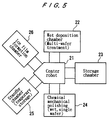
- FIG. 5 shows a schematic diagram of a substrate surface protection apparatus applied to a facility that include process lines for semiconductor wafers by wet-process film forming and wet polishing processes.
- a central robot 21 is surrounded by a wet-process film forming chamber 22 for forming films on a plurality of substrates at a time; a storage chamber 23 for storing a plurality of substrates; a wet-process polishing chamber 24 for processing a wafer at a time; a standby chamber 25 for holding the substrates temporarily and an ice film coating chamber 26 for forming an ice film on the substrate which is the surface protection apparatus according to the present invention.
- the processed wafers is treated in the ice forming chamber 26 to be coated with an ice film.
- This treatment provides a protection of a processed surface by preventing the as-processed surface to be exposed to the ambient atmosphere to result in degradation and contamination of the surface, thereby preserving the conditions of the processed surface that has undergone a given process and has reached a certain desired surface condition.
- the material for protecting the surface should be chosen so that the coating prevents contact with the process room atmosphere but the coating also should not chemically react with the substrate material and is harmless mechanically, and permits easy melting and removal. From such viewpoints, water fulfills all the requirements, and immersion in warmer water removes the ice film instantly so that water is an ideal material.
- the flowchart shown in Figure 6 is an example of using the facility in Figure 5.
- a plurality of substrates may be treated concurrently in the wet-process film forming chamber 22 (step 1), followed by processing in the ice film coating chamber 26 to envelop the substrates with ice film (step 2), and the ice-coated wafers are placed in standby for temporary storage (step 3).
- the wet-process polishing chamber one wafer at a time is polished (step 4), and the polished wafer is stored in the storage chamber 23 (step 5).
- the stored wafers in step 3 may be sent back to the ice film coating chamber 26 to be coated with ice film, followed by further treatments in the wet-process film forming chamber 22.
- the wafers after polishing in step 4 may be sent to the ice film coating chamber 26 to be coated with ice, and may be stored temporarily in the standby room 25.
- the wafers are often required to spend sometime waiting for the next unit processing because of the differences in processing factors, such as the processing times of film forming and polishing processes, number of wafer that can be treated at a time, and process productivity. Because the processing is carried out in a process room environment, the conventional standby approach increases the length of time for the wafers to be exposed to the surrounding atmosphere. However, using the process shown in Figure 6, the surfaces can be protected by ice coating, when necessary, so that potential problems of surface degradation and contamination caused by contact with the surrounding atmosphere are significantly reduced.
- the approach (1) described above is susceptible to high energy consumption and long processing times, because of the natural tendency to form a thick water layer dictated by natural requirements.
- the advantage is that the apparatus can be relatively simple.
- the approach (2) requires a complex apparatus, the advantages are that the film thickness is thin and the processing time is very short. Therefore, the two approaches should be used alternatively to suit the processing requirements so that the surface protection can be practiced to suit the needs of the main processing procedure.
- the quality of water used in the present invention should be chosen to be compatible with the use and nature of the substrate material. Especially, for use in protecting semiconductor devices, ultrapure water would generally be chosen. Also, the present method is most suitable to wet-process film forming and polishing processes carried out under normal processing environment, rather than for vacuum processes.
Landscapes
- Engineering & Computer Science (AREA)
- Physics & Mathematics (AREA)
- Condensed Matter Physics & Semiconductors (AREA)
- General Physics & Mathematics (AREA)
- Manufacturing & Machinery (AREA)
- Computer Hardware Design (AREA)
- Microelectronics & Electronic Packaging (AREA)
- Power Engineering (AREA)
- Container, Conveyance, Adherence, Positioning, Of Wafer (AREA)
- Mechanical Treatment Of Semiconductor (AREA)
Applications Claiming Priority (2)
| Application Number | Priority Date | Filing Date | Title |
|---|---|---|---|
| JP16946398 | 1998-06-17 | ||
| JP10169463A JP2000012648A (ja) | 1998-06-17 | 1998-06-17 | 素子製造工程における基材表面保護方法及び装置 |
Publications (2)
| Publication Number | Publication Date |
|---|---|
| EP0966024A2 true EP0966024A2 (fr) | 1999-12-22 |
| EP0966024A3 EP0966024A3 (fr) | 2005-01-05 |
Family
ID=15887046
Family Applications (1)
| Application Number | Title | Priority Date | Filing Date |
|---|---|---|---|
| EP99111089A Withdrawn EP0966024A3 (fr) | 1998-06-17 | 1999-06-17 | Méthode et appareil pour la protection de la surface d'un substrat |
Country Status (5)
| Country | Link |
|---|---|
| US (1) | US6573201B1 (fr) |
| EP (1) | EP0966024A3 (fr) |
| JP (1) | JP2000012648A (fr) |
| KR (1) | KR20000006236A (fr) |
| TW (1) | TW426852B (fr) |
Families Citing this family (8)
| Publication number | Priority date | Publication date | Assignee | Title |
|---|---|---|---|---|
| KR100853000B1 (ko) * | 2001-03-16 | 2008-08-19 | 신에쯔 한도타이 가부시키가이샤 | 실리콘 웨이퍼 보관용수 및 보관방법 |
| JP4567622B2 (ja) * | 2006-03-15 | 2010-10-20 | 富士通セミコンダクター株式会社 | 半導体ウェハの保管方法 |
| DE102006038243A1 (de) * | 2006-08-14 | 2008-02-28 | Qimonda Ag | Verfahren und Einrichtung zum Handhaben eines Gegenstandes im Rahmen einer Halbleiterfertigung |
| US7933000B2 (en) * | 2006-11-16 | 2011-04-26 | Asml Netherlands B.V. | Device manufacturing method, method for holding a patterning device and lithographic apparatus including an applicator for applying molecules onto a clamp area of a patterning device |
| JP2022523709A (ja) | 2019-01-29 | 2022-04-26 | ラム リサーチ コーポレーション | 基板の環境に敏感な表面のための犠牲保護層 |
| KR102665933B1 (ko) | 2020-05-12 | 2024-05-20 | 램 리써치 코포레이션 | 자극-반응성 폴리머 막의 제어된 열화 |
| US20230178364A1 (en) * | 2020-07-02 | 2023-06-08 | Lam Research Corporation | Removable cvd polymer film for surface protection and queue period extension |
| WO2024081174A1 (fr) * | 2022-10-10 | 2024-04-18 | Lam Research Corporation | Copolymères d'oxyméthylène pour protection de surface transitoire lors d'un dépôt chimique en phase vapeur |
Citations (5)
| Publication number | Priority date | Publication date | Assignee | Title |
|---|---|---|---|---|
| US4156040A (en) * | 1976-05-12 | 1979-05-22 | Ford Motor Company | Coagulation coating process |
| EP0273628A1 (fr) * | 1986-12-17 | 1988-07-06 | Fujitsu Limited | Procédé de production de dispositifs semi-conducteurs |
| WO1989010803A1 (fr) * | 1988-05-03 | 1989-11-16 | Regents Of The University Of Minnesota | Procede de nettoyage de surface et de fluide |
| EP0423761A2 (fr) * | 1989-10-17 | 1991-04-24 | Applied Materials, Inc. | Dispositif et méthode pour enlever des particules avec fluide de convection forcée |
| JPH03261142A (ja) * | 1990-03-12 | 1991-11-21 | Fujitsu Ltd | 半導体基板洗浄方法 |
Family Cites Families (14)
| Publication number | Priority date | Publication date | Assignee | Title |
|---|---|---|---|---|
| JPS5417450B2 (fr) * | 1974-05-17 | 1979-06-29 | ||
| US3918267A (en) * | 1974-11-18 | 1975-11-11 | Gen Motors Corp | Ice-maker control circuit with slab limiting control |
| US4281031A (en) * | 1979-07-25 | 1981-07-28 | Machine Technology, Inc. | Method and apparatus for processing workpieces |
| US4430150A (en) * | 1981-08-07 | 1984-02-07 | Texas Instruments Incorporated | Production of single crystal semiconductors |
| GB2129018B (en) * | 1982-08-30 | 1986-01-29 | Ricoh Kk | Vacuum evaporation apparatus |
| US4951601A (en) * | 1986-12-19 | 1990-08-28 | Applied Materials, Inc. | Multi-chamber integrated process system |
| DE4010663C2 (de) * | 1990-04-03 | 1998-07-23 | Leybold Ag | Vorrichtung und Verfahren zur plasmagestützten Beschichtung von Werkstücken |
| US5976198A (en) * | 1995-06-09 | 1999-11-02 | Dainippon Screen Mfg. Co., Ltd. | Substrate transfer and bath apparatus |
| US5787723A (en) * | 1995-08-21 | 1998-08-04 | Manitowoc Foodservice Group, Inc. | Remote ice making machine |
| US5763010A (en) * | 1996-05-08 | 1998-06-09 | Applied Materials, Inc. | Thermal post-deposition treatment of halogen-doped films to improve film stability and reduce halogen migration to interconnect layers |
| DE19716374A1 (de) * | 1997-04-18 | 1998-10-22 | Wacker Chemie Gmbh | Brechen von Reinstsilicium auf Eis |
| US6110011A (en) * | 1997-11-10 | 2000-08-29 | Applied Materials, Inc. | Integrated electrodeposition and chemical-mechanical polishing tool |
| DE19755975A1 (de) * | 1997-12-16 | 1999-06-17 | Wolters Peter Werkzeugmasch | Halter für flache Werkstücke, insbesondere Halbleiterwafer |
| US6132289A (en) * | 1998-03-31 | 2000-10-17 | Lam Research Corporation | Apparatus and method for film thickness measurement integrated into a wafer load/unload unit |
-
1998
- 1998-06-17 JP JP10169463A patent/JP2000012648A/ja active Pending
-
1999
- 1999-06-15 US US09/332,904 patent/US6573201B1/en not_active Expired - Fee Related
- 1999-06-16 TW TW088110057A patent/TW426852B/zh not_active IP Right Cessation
- 1999-06-17 EP EP99111089A patent/EP0966024A3/fr not_active Withdrawn
- 1999-06-17 KR KR1019990022663A patent/KR20000006236A/ko not_active Application Discontinuation
Patent Citations (5)
| Publication number | Priority date | Publication date | Assignee | Title |
|---|---|---|---|---|
| US4156040A (en) * | 1976-05-12 | 1979-05-22 | Ford Motor Company | Coagulation coating process |
| EP0273628A1 (fr) * | 1986-12-17 | 1988-07-06 | Fujitsu Limited | Procédé de production de dispositifs semi-conducteurs |
| WO1989010803A1 (fr) * | 1988-05-03 | 1989-11-16 | Regents Of The University Of Minnesota | Procede de nettoyage de surface et de fluide |
| EP0423761A2 (fr) * | 1989-10-17 | 1991-04-24 | Applied Materials, Inc. | Dispositif et méthode pour enlever des particules avec fluide de convection forcée |
| JPH03261142A (ja) * | 1990-03-12 | 1991-11-21 | Fujitsu Ltd | 半導体基板洗浄方法 |
Non-Patent Citations (1)
| Title |
|---|
| PATENT ABSTRACTS OF JAPAN vol. 016, no. 067 (E-1168), 19 February 1992 (1992-02-19) -& JP 03 261142 A (FUJITSU LTD), 21 November 1991 (1991-11-21) * |
Also Published As
| Publication number | Publication date |
|---|---|
| US6573201B1 (en) | 2003-06-03 |
| TW426852B (en) | 2001-03-21 |
| KR20000006236A (ko) | 2000-01-25 |
| JP2000012648A (ja) | 2000-01-14 |
| EP0966024A3 (fr) | 2005-01-05 |
Similar Documents
| Publication | Publication Date | Title |
|---|---|---|
| US4985372A (en) | Method of forming conductive layer including removal of native oxide | |
| EP0535354A1 (fr) | Méthode de fabrication d'une couche de nitrure utilisant de l'ammoniac préchauffé | |
| US20080047490A1 (en) | Vapor deposition of benzotriazole (BTA) for protecting copper interconnects | |
| US20140302254A1 (en) | Plasma cleaning method | |
| US20120178263A1 (en) | Substrate processing apparatus | |
| US6573201B1 (en) | Method and apparatus for protection of substrate surface | |
| US6214425B1 (en) | Storage box for an object to be protected against physicochemical contamination | |
| JPH1112738A (ja) | Cvd成膜方法 | |
| US8147909B2 (en) | Method of making and using alloy susceptor with improved properties for film deposition | |
| CA1316273C (fr) | Methode de stockage de substrats semiconducteurs | |
| JP2003115519A (ja) | 半導体装置の製造方法、半導体製造装置、ロードロック室、基板収納ケース、ストッカ | |
| JP3058909B2 (ja) | クリーニング方法 | |
| US20130217207A1 (en) | Method for directly adhering two plates together, including a step of forming a temporary protective nitrogen layer | |
| JPS61292922A (ja) | 半導体装置の製造方法 | |
| US7489494B2 (en) | Guard wafer for semiconductor structure fabrication | |
| US6202423B1 (en) | Non-damage transport system by ice condensation | |
| JPH0864666A (ja) | 基板収納容器及び基板処理方法 | |
| JPH0786170A (ja) | 枚葉式ホットウォール処理装置及びそのクリーニング方法 | |
| JPH07227534A (ja) | 真空容器の圧力制御方法 | |
| JPH0786172A (ja) | 処理用ガスの供給方法 | |
| CN116377413A (zh) | 一种生长硅薄膜的工艺方法及半导体设备 | |
| JP5077155B2 (ja) | 成膜装置及びそのクリーニング方法 | |
| JP2000160322A (ja) | スパッタリング方法及び装置 | |
| JPH03171626A (ja) | 半導体基体の処理方法 | |
| JPH02298270A (ja) | 成膜方法 |
Legal Events
| Date | Code | Title | Description |
|---|---|---|---|
| PUAI | Public reference made under article 153(3) epc to a published international application that has entered the european phase |
Free format text: ORIGINAL CODE: 0009012 |
|
| AK | Designated contracting states |
Kind code of ref document: A2 Designated state(s): AT BE CH CY DE DK ES FI FR GB GR IE IT LI LU MC NL PT SE |
|
| AX | Request for extension of the european patent |
Free format text: AL;LT;LV;MK;RO;SI |
|
| PUAL | Search report despatched |
Free format text: ORIGINAL CODE: 0009013 |
|
| AK | Designated contracting states |
Kind code of ref document: A3 Designated state(s): AT BE CH CY DE DK ES FI FR GB GR IE IT LI LU MC NL PT SE |
|
| AX | Request for extension of the european patent |
Extension state: AL LT LV MK RO SI |
|
| 17P | Request for examination filed |
Effective date: 20050705 |
|
| AKX | Designation fees paid |
Designated state(s): DE FR GB |
|
| 17Q | First examination report despatched |
Effective date: 20070605 |
|
| STAA | Information on the status of an ep patent application or granted ep patent |
Free format text: STATUS: THE APPLICATION IS DEEMED TO BE WITHDRAWN |
|
| 18D | Application deemed to be withdrawn |
Effective date: 20071218 |