EP0960738B1 - Semiconductor-chip control apparatus and control method and image recording apparatus and its control method - Google Patents
Semiconductor-chip control apparatus and control method and image recording apparatus and its control method Download PDFInfo
- Publication number
- EP0960738B1 EP0960738B1 EP99110380A EP99110380A EP0960738B1 EP 0960738 B1 EP0960738 B1 EP 0960738B1 EP 99110380 A EP99110380 A EP 99110380A EP 99110380 A EP99110380 A EP 99110380A EP 0960738 B1 EP0960738 B1 EP 0960738B1
- Authority
- EP
- European Patent Office
- Prior art keywords
- base substrate
- recording
- semiconductor chip
- light
- electrode
- Prior art date
- Legal status (The legal status is an assumption and is not a legal conclusion. Google has not performed a legal analysis and makes no representation as to the accuracy of the status listed.)
- Expired - Lifetime
Links
- 238000000034 method Methods 0.000 title claims description 14
- 239000004065 semiconductor Substances 0.000 claims description 55
- 239000000758 substrate Substances 0.000 claims description 51
- 238000012546 transfer Methods 0.000 claims description 41
- 150000002500 ions Chemical class 0.000 claims description 10
- 239000000853 adhesive Substances 0.000 claims description 9
- 230000001070 adhesive effect Effects 0.000 claims description 9
- BQCADISMDOOEFD-UHFFFAOYSA-N Silver Chemical compound [Ag] BQCADISMDOOEFD-UHFFFAOYSA-N 0.000 description 7
- 229910052709 silver Inorganic materials 0.000 description 7
- 239000004332 silver Substances 0.000 description 7
- 238000000151 deposition Methods 0.000 description 4
- 230000008021 deposition Effects 0.000 description 3
- 238000011161 development Methods 0.000 description 3
- 230000018109 developmental process Effects 0.000 description 3
- 238000010586 diagram Methods 0.000 description 3
- 230000005684 electric field Effects 0.000 description 3
- 239000004593 Epoxy Substances 0.000 description 2
- 230000008901 benefit Effects 0.000 description 2
- 239000000919 ceramic Substances 0.000 description 2
- 230000007423 decrease Effects 0.000 description 2
- 239000011521 glass Substances 0.000 description 2
- 239000000463 material Substances 0.000 description 2
- 238000012986 modification Methods 0.000 description 2
- 230000004048 modification Effects 0.000 description 2
- 229910001218 Gallium arsenide Inorganic materials 0.000 description 1
- 230000008859 change Effects 0.000 description 1
- 238000004891 communication Methods 0.000 description 1
- 230000001419 dependent effect Effects 0.000 description 1
- 238000013461 design Methods 0.000 description 1
- 230000004907 flux Effects 0.000 description 1
- 239000012535 impurity Substances 0.000 description 1
- 238000004519 manufacturing process Methods 0.000 description 1
- 229910021645 metal ion Inorganic materials 0.000 description 1
- 230000003287 optical effect Effects 0.000 description 1
- 230000008569 process Effects 0.000 description 1
- 238000012545 processing Methods 0.000 description 1
Images


Classifications
-
- B—PERFORMING OPERATIONS; TRANSPORTING
- B41—PRINTING; LINING MACHINES; TYPEWRITERS; STAMPS
- B41J—TYPEWRITERS; SELECTIVE PRINTING MECHANISMS, i.e. MECHANISMS PRINTING OTHERWISE THAN FROM A FORME; CORRECTION OF TYPOGRAPHICAL ERRORS
- B41J2/00—Typewriters or selective printing mechanisms characterised by the printing or marking process for which they are designed
- B41J2/435—Typewriters or selective printing mechanisms characterised by the printing or marking process for which they are designed characterised by selective application of radiation to a printing material or impression-transfer material
- B41J2/447—Typewriters or selective printing mechanisms characterised by the printing or marking process for which they are designed characterised by selective application of radiation to a printing material or impression-transfer material using arrays of radiation sources
- B41J2/45—Typewriters or selective printing mechanisms characterised by the printing or marking process for which they are designed characterised by selective application of radiation to a printing material or impression-transfer material using arrays of radiation sources using light-emitting diode [LED] or laser arrays
-
- H—ELECTRICITY
- H10—SEMICONDUCTOR DEVICES; ELECTRIC SOLID-STATE DEVICES NOT OTHERWISE PROVIDED FOR
- H10F—INORGANIC SEMICONDUCTOR DEVICES SENSITIVE TO INFRARED RADIATION, LIGHT, ELECTROMAGNETIC RADIATION OF SHORTER WAVELENGTH OR CORPUSCULAR RADIATION
- H10F30/00—Individual radiation-sensitive semiconductor devices in which radiation controls the flow of current through the devices, e.g. photodetectors
- H10F30/20—Individual radiation-sensitive semiconductor devices in which radiation controls the flow of current through the devices, e.g. photodetectors the devices having potential barriers, e.g. phototransistors
Definitions
- the present invention relates to a base substrate comprising a semiconductor chip such as an LED array used as a recording light-emitting element and a control apparatus for controlling the semiconductor chip, moreover to an image recording apparatus for forming a visible image on a recording medium through an electrophotographic recording system by using the semiconductor chip, and to a control method for controlling the semiconductor chip being mounted on a base substrate comprised in an image recording apparatus.
- a self-scanning LED array (hereafter referred to as SLED) has been used so far as a recording light-emitting element.
- EP 0 335 553 discloses a SLED comprising a coupled array of light-emitting elements constituted so that a light-emitting element which is turned on influences another light-emitting element to be turned on next so that its threshold level is changed.
- Another self-scanning LED array is disclosed in Japanese Patent Application Laid-Open Nos. 1-238962, 2-208067, 2-212170, 3-20457, 3-194978, 4-5872, 4-23367, 4-296579, and 5-84971, JAPAN HARD COPY, proposal of optical-printer light emitting array constituted by integrating 91 (A-17) driving circuit, and proposal of self-scanning light-emitting element (SLED) using the PNPN thyristor structure of IEICE (Institute of Electronics, Information and Communication Engineers), March 5, 1990, and noticed as a recording light-emitting element.
- SLED self-scanning light-emitting element
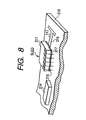
- FIG. 8 shows a schematic configuration of the SLED array head.
- Symbol 211 denotes an SLED semiconductor chip.
- Symbol 212 denotes a base substrate for mounting the SLED semiconductor chip 211, which is configured by a printed circuit board made of glass epoxy or ceramic.
- Symbol 214 denotes a driver IC for receiving a control signal from an external unit to generate a driving signal for the SLED semiconductor chip 211.
- Symbol 215 denotes a bonding wire for connecting output signals supplied from the driver IC 214 ( ⁇ 1, ⁇ 2, ⁇ S, and ⁇ I) and a negative-electrode-side power-supply input (GND as for this embodiment) to the SLED semiconductor chip 211 respectively.
- Symbol 216 denotes a positive-electrode (+) power-supply pattern extended to the base substrate 212 (+5V as for this embodiment).
- Symbol 217 denotes silver paste for electrically connecting and bonding the positive-electrode-side power-supply pattern 216 extended to the base substrate 212 with the back-face electrode of the SLED semiconductor chip 211 to fix them.
- the SLED semiconductor chip 211 frequently uses a method of using the substrate of a chip as an anode because anodes of a light-emission thyristor and a transfer thyristor both serve as a common line and thereby, serve a maximum operating-current route and due to electrical characteristics of P and N of a semiconductor (generally, GaAs semiconductor is used) and problems on fabrication process.
- a semiconductor generally, GaAs semiconductor is used
- a substrate normally serves as a positive electrode.
- the substrate is electrically connected with the power-supply pattern 216 of the base substrate 212 by the silver paste 217 through a back-face electrode or the like.
- an electric-field configuration is formed in which positive ions in the substrate-side silver paste 217 (conductive adhesive) are attracted to the epitaxial-layer side through a chip-side face or the like at a portion serving as a negative electrode in the signal input unit of the epitaxial-layer-side face of the SLED semiconductor chip 211 configuring a circuit opposite to the substrate-side face of the SLED semiconductor chip 211.
- the distance between the signal input unit on the epitaxial-layer-side face and the silver paste 217 at the substrate side is approximately 600 ⁇ m.
- the attracted positive ions are deposited through reaction with other impurity ions. Therefore, if the deposition reaction continuously occurs, a short circuit is formed between the epitaxial-layer and the substrate due to reasonable elapse of time and thereby, the original operation of an SLED can not be performed.
- a control signal input unit (control signals ⁇ 1, ⁇ 2, ⁇ S, and ⁇ I) and a negative-electrode-side power-supply input unit (negative-electrode-potential on/off control signal ⁇ m) are fixed to a potential or high-impedance state same as that of a positive-electrode-side power-supply input unit (power-supply voltage of +5V) in a predetermined period in which light-emitting operation or transfer operation is not performed by an LED (Light-Emitting Diode) array.
- a control signal input unit (control signals ⁇ 1, ⁇ 2, ⁇ S, and ⁇ I), a positive-electrode-side power-supply input unit (positive-electrode potential on/off control signal ⁇ p), and a negative-electrode-side power-supply input unit (GND) are fixed to the same potential or high-impedance state in a predetermined period in which the light-emitting operation or transfer operation is not performed by an LED array.
- FIGS. 1 to 5 The first embodiment of the present invention will be described below by referring to FIGS. 1 to 5. However, the description of a portion same as that of a conventional example is omitted and the portion is provided with the same symbol.
- FIGS. 1 to 3 A schematic configuration of the first embodiment will be described by referring to FIGS. 1 to 3.
- FIG. 1 shows a schematic configuration of a substrate mounting a self-scanning LED (SLED) array head of the present invention.
- FIG. 2 shows an enlarged circuit configuration of an SLED semiconductor chip 211.
- FIG. 3 shows the appearance of a substrate including an SLED array head.
- SLED self-scanning LED
- symbol 211 denotes an SLED semiconductor chip.
- symbols 1 to 5 denote light-emitting thyristors serving as recording elements and 11 to 15 denote transfer thyristors.
- a +5V power-supply line 50 is connected to anodes and a connection line 20 to which image data ⁇ D and a control signal ⁇ I are inputted is connected to cathodes.
- the +5V power-supply line 50 is connected to the anodes and connection lines 21 and 22 to which shift pulses 1 and 2 serving as control signals ⁇ 1 and ⁇ 2 are inputted are connected to the cathodes.
- Gate terminals of the light-emitting thyristors 1 to 5 are connected with gate terminals of the transfer thyristors 11 to 15 by connection lines 31 to 35 respectively.
- Diodes 41 to 45 are connected between the connection lines 31 to 35 in series.
- connection line 23 to which a start pulse ⁇ s is inputted is connected to a connection point "a" with a diode 41 of the connection line 31.
- connection lines 31 to 35 are connected with a connection line 51 to which a negative-electrode-potential on/off control signal ⁇ m is inputted.
- the connection line 51 is connected with the collector terminal of a switching element 201.
- a connection line 52 to which the negative-electrode-potential on/off control signal ⁇ m is inputted is connected to the base terminal of the switching element 201.
- Symbol 212 denotes a base substrate for mounting the SLED semiconductor chip 211.
- the SLED semiconductor chip 211 is configured by a printed circuit board made of glass epoxy or ceramic.
- Symbol 213 denotes a connector.
- the connector 213 connects with the connection line 52 for the negative-electrode-potential on/off control signal ⁇ m, connection lines 20 to 23 for the control signals ⁇ 1, ⁇ 2, ⁇ S, and ⁇ I, +5V power-supply line 50, and earth line 53.
- Symbol 214 denotes a driver IC for receiving various control signals from external units and outputting these signals as control signals for driving the SLED semiconductor chip 211.
- symbol 215 denotes a bonding wire for connecting control signals ( ⁇ 1, ⁇ 2, ⁇ S, and ⁇ I) outputted from the driver IC 214 and a negative-electrode-side power-supply input signal (as for this embodiment, GND supplied from the earth line 53) to an electrode formed on the surface of the SLED semiconductor chip 211.
- Symbol 216 denotes a positive-electrode-side power-supply pattern (+5V as for this embodiment) extended to the base substrate 212.
- Symbol 217 denotes silver paste for electrically connecting and bonding the positive-electrode-side power-supply pattern 216 extended to the base substrate 212 with the back-face electrode of the SLED semiconductor chip 211 and bonding to fix them.
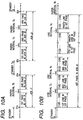
- FIG. 4 shows operation timings of various control signals ⁇ 1, ⁇ 2, ⁇ S, and ⁇ I for controlling light emission and non-light emission of the light-emission thyristors 1 to 5 in the SLED semiconductor chip 211 and a negative-electrode-potential on/off control signal ⁇ m.
- the hatched region enclosed by broken lines shown by the waveform of the image data ⁇ D shows a state in which the light-emission thyristors 1 to 5 are turned on.
- the portion of a section T1 is a waveform when the normal light-emitting or transfer operation is performed (detailed operations are described later).
- the portion of a section T2 corresponds to a predetermined period in which the light-emitting or transfer operation by an LED array is not performed and which is a feature of this embodiment.
- a control signal input unit (control signals ⁇ 1, ⁇ 2, ⁇ S, and ⁇ I) and a negative-electrode-side power-supply input unit (negative-electrode potential on/off control signal ⁇ m) are fixed to a potential or high-impedance state same as that of a positive-electrode-side power-supply input unit (power-supply voltage of +5V) in the predetermined section T2.
- the final portion of the section T1 denotes the timing of the final step of a series of light-emitting operations of a unit mounting an SLED array head. That is, the subsequent section denotes a state in which no light-emitting or transfer operation is requested.
- the subsequent section T2 denotes a section of the present invention.
- the control signals ⁇ 1, ⁇ 2, ⁇ S, and ⁇ I are all fixed to +5V.
- the negative-electrode-potential on/off control signal ⁇ m is set to 0V and input, the switching element 201 is turned off, and thereby, the negative-electrode-side power supply is opened.
- every signal and negative-electrode-side power supply connected to the epitaxial-layer-side face (element-forming face) of the SLED semiconductor chip 211 opposite to the substrate-side face (back-face electrode side) is set to a potential equal to that of the positive-electrode-side power supply of the substrate side or a floating state and thus, a state in which a bias is not applied between the substrate and the epitaxial-layer is configured.
- the conductive ion component of the silver paste 217 serving as a conductive adhesive for connecting the substrate of the SLED semiconductor chip 211 with the base substrate 212 of the chip 211 and fixing them is moved in the epitaxial-layer direction and thus, it is possible to prevent a phenomenon such as deposition from occurring.
- an LED array head that performs recording by mounting an SLED array head including the SLED semiconductor chip 211 on an image-forming unit according to an electrostatic electrophotographic system.
- the ratio of the total standby time until the service life of the body expires to the actual working time of the body is considerably large. Because the time ratio is considerably large, it is possible to control the time for depositing an ion component and thereby, it is possible to improve the deposition quantity based on the ion component up to a level at which no problem occurs in practical use.
- this embodiment controls the negative-electrode-potential on/off control signal ⁇ m and the control signals ⁇ 1, ⁇ 2, ⁇ S, and ⁇ I so as to perform circuit operations.
- the circuit configuration for generating these various signals is omitted. Basically, however, it is possible to execute a predetermined processing by using software means by a control program or hardware means by an arithmetic circuit such as a delay circuit and thereby, performing general control by a CPU.
- FIG. 5 shows control signals for controlling the SLED and their timings, which is an example when turning on every element.
- the SLED is configured by the transfer thyristors 11 to 15 arranged like an array and the light-emission thyristors 1 to 5 arranged like an array. Gates of the thyristors are connected each other and the first thyristor is connected to the ⁇ S-signal input unit. The gate of the second thyristor is connected to the cathode of the diode 41 connected to the ⁇ S terminal and the third thyristor is connected to the cathode of the next diode 42.
- Transfer is started by changing ⁇ S from 0V to 5V.
- ⁇ S is changed to 5V
- Va is set to 5V
- Vb is set to 3.7V (when assuming that the forward-directional voltage drop of a diode is 1.3V)
- Vc is set to 2.4V
- Vd is set to 1.1V
- gate signals of the transfer thyristors 11 and 12 change from 0V to 5V and 3.7V respectively.
- the potential of the anode of the transfer thyristor 11 is set to 5V, that of the cathode of it is set to 0V, that of the gate of it is set to 3.7V, thereby the on-condition of the thyristor is set, and thus the transfer thyristor 11 is turned on.
- Va is set to approximately 5V because the thyristor 11 is turned on (this is because a pulse is applied to ⁇ S through a resistance and when the thyristor is turned on, potentials of the anode and gate becomes almost equal). Therefore, even if setting ⁇ S to 0V, the on-condition of the first thyristor is kept and the first shift operation is completed.
- the gate voltage Va of the transfer thyristor 11 is set to approximately 5V and the voltage Vb is set to 3.7V.
- the potential of the anode of the transfer thyristor 12 is set to 5V, that of the cathode of it is set to 0V, and that of the gate of it is set to 3.7V, and the transfer thyristor 12 is turned on.
- the transfer thyristor 11 is turned off the same as the light-emission thyristor 1 is turned off.
- on-state is transferred from the transfer thyristor 11 to the transfer thyristor 12.
- ⁇ I from 5V to 0V
- the light-emission thyristor 2 is turned on to emit light.
- the thyristor next to the turned-on thyristor is not turned on because the light-emission thyristor is turned on, thereby the potential of ⁇ I is set to 3.4V (equivalent to the forward voltage drop of the light-emission thyristor), and the potential difference between the gate and the cathode of the thyristor next to the turned-on thyristor decreases to 0.
- FIG. 6 shows a schematic configuration of a substrate mounting an SLED array head of the present invention.
- connection line 51 is connected to the earth.
- Other configuration is the same as that of the first embodiment above described.
- a control line 60 for inputting a positive-electrode-potential on/off control signal ⁇ p is connected to a connector 213.
- the control line 60 is connected to the gate terminal of a switching element 61 and each three-state buffer 62 in a driver IC 214.
- the positive-electrode-potential on/off control signal ⁇ p substitutes for the negative-electrode-potential on/off control signal ⁇ m.
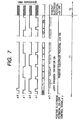
- FIG. 7 shows operation timings of the control signals ⁇ 1, ⁇ 2, ⁇ S, and ⁇ I, and the positive-electrode-potential on/off control signal ⁇ p for controlling light emission and non-light emission of the light-emission thyristors 1 to 5 in the SLED semiconductor chip 211.
- the portion of the section T2 corresponds to a predetermined period in which the light-emitting operation or transfer operation is not performed by an LED array and which is a feature of this embodiment.
- the portion of the section T1 shows a waveform while the normal light-emitting or transfer operation is performed, which is the same as the example above described.
- control signal input unit ( ⁇ 1, ⁇ 2, ⁇ S, and ⁇ I), positive-electrode power-supply input unit (positive-electrode-potential on/off control signal ⁇ p), and negative-electrode power-supply input unit (GND) are set to the same potential or high-impedance state in the predetermined section T2.
- the section T1 is a section when the normal light-emitting or transfer operation is performed.
- the portion of the section T1 is assumed as the timing of the final step of a series of light-emitting operations of a unit mounting an SLED array head. That is, thereafter, a state in which next light-emitting or transfer operation is not requested is kept.
- the section T2 following the section T1 is a section in which characteristic operations of this embodiment are performed.
- the control signals ⁇ 1, ⁇ 2, ⁇ S, and ⁇ I are turned off by turning off the three-state buffer 62 in accordance with the positive-electrode-potential on/off control signal ⁇ p corresponding to the disabling notice of an enable signal supplied from an external unit.
- the positive-electrode-side power supply (+5V) is simultaneously turned off by turning off the switching element 61 in accordance with the positive-electrode-potential on/off control signal ⁇ p.
- every signal connected to the epitaxial-layer-side face (element-forming face) of the SLED semiconductor chip 211 is set to a high-impedance state. Moreover, because the portion between the negative and positive electrodes is set to zero volt, a state in which no bias is applied between the substrate and the epitaxial-layer is configured.
- every control signal and a negative-electrode-side power-supply input unit are set to a potential or high-impedance state same as that of a positive-electrode-side power-supply input unit in a predetermined period in which the light-emitting or transfer operation is not performed by a light-emitting element or every control signal, the positive-electrode-side power-supply input unit, and the negative-electrode-side power-supply input unit are the same potential of high-impedance state.
- FIG. 9 is a sectional view of the image recording apparatus. Because the configuration and control operations of the SLED array head were previously described, other portions will be described below.
- symbol 212 denotes the above-described base substrate on which an SLED chip 211 is mounted.
- the light-emitting unit of the SLED chip 211 is turned downward in FIG. 9.
- Symbol 902 denotes a photosensitive body rotating in the direction of the arrow and 903 denotes a self-focusing lens array.
- the lens array 903 records an electrostatic latent image on the photosensitive-body drum 902 by focusing a luminous flux emitted from the SLED chip 211 on the faced photosensitive-body drum 902.
- the base substrate 212 and the lens array 903 are integrated as a removable cartridge and the cartridge including the base substrate 212 and the lens array 903 may be referred to as an SLED array head 901.
- symbol 904 denotes a primary electrification roller for uniformly electrifying the surface of the photosensitive-body drum 902 before exposure by the SLED array head 901 and 905 denotes a development counter for developing an electrostatic latent image recorded on the photosensitive-body drum 902 with toner by the SLED array head 901, 906 denotes a transfer roller for transferring the toner image recorded by the development counter 905 onto a transfer form, and 907 denotes a fixing unit for fixing the toner image on the transfer sheet.
- each section in the image control unit is controlled by a control unit 908.
- An operation unit 909 is used for an operator to supply a command for starting an image recording job or the like to an image recording apparatus 900.
- an image readout apparatus 910 is connected as the external unit of the image recording apparatus 900 and moreover connected with a host computer 920 through a network 921. Thereby, the image recording apparatus 900 can execute various image recording jobs on an image read by the image readout apparatus 910 or languaged image information to be sent from the host computer.
- FIG. 10A shows a case of performing an image recording job J1 for two pages and an image recording job J2 for three pages.
- symbol tj1s denotes the timing when the image recording job J1 is started
- tj1e denotes the timing when the image recording job J1 is ended
- tj2s denotes the timing when the image recording job J2 is started
- tj2e denotes the timing when the image recording job J2 is ended.
- the above section T2 is controlled at the timing of standby Ta between the image recording jobs (that is, in a period between tj1e and tj2s).
- control unit 908 executes the control of the above section T2 during the standby between the image recording jobs and thereafter, changes the mode to the control of the above section T1 to execute an image recording job synchronously with an image-recording-jog start command supplied from the operation unit 909 or host computer 920. Moreover, the control unit 908 changes the mode to the control of the above section T2 again after the image recording job is completed.
- FIG. 10B shows a detailed timing chart while the image on each page is recorded.
- This embodiment makes it possible to record data on a recording medium such as a photosensitive body by mounting the above head on an electrophotographic image recording apparatus as a recording head and thereby, it is possible to fabricate a recording apparatus having less electrical troubles and a high reliability when recording operation is performed.
- an SLED array chip is used as a semiconductor chip.
- the present invention is not restricted to the above case. It is apparent that the present invention can be applied to a recording-element array chip other than a light-emitting-element array chip and moreover, various semiconductor chips other than a semiconductor chip used for recording.
Landscapes
- Physics & Mathematics (AREA)
- Optics & Photonics (AREA)
- Health & Medical Sciences (AREA)
- General Health & Medical Sciences (AREA)
- Toxicology (AREA)
- Printers Or Recording Devices Using Electromagnetic And Radiation Means (AREA)
- Led Devices (AREA)
- Led Device Packages (AREA)
Applications Claiming Priority (2)
| Application Number | Priority Date | Filing Date | Title |
|---|---|---|---|
| JP14901198A JPH11340498A (ja) | 1998-05-29 | 1998-05-29 | 駆動制御装置および画像記録装置 |
| JP14901198 | 1998-05-29 |
Publications (3)
| Publication Number | Publication Date |
|---|---|
| EP0960738A2 EP0960738A2 (en) | 1999-12-01 |
| EP0960738A3 EP0960738A3 (en) | 2000-03-22 |
| EP0960738B1 true EP0960738B1 (en) | 2005-12-28 |
Family
ID=15465732
Family Applications (1)
| Application Number | Title | Priority Date | Filing Date |
|---|---|---|---|
| EP99110380A Expired - Lifetime EP0960738B1 (en) | 1998-05-29 | 1999-05-28 | Semiconductor-chip control apparatus and control method and image recording apparatus and its control method |
Country Status (5)
| Country | Link |
|---|---|
| US (1) | US6624838B2 (enExample) |
| EP (1) | EP0960738B1 (enExample) |
| JP (1) | JPH11340498A (enExample) |
| KR (1) | KR100294952B1 (enExample) |
| DE (1) | DE69929112T2 (enExample) |
Families Citing this family (8)
| Publication number | Priority date | Publication date | Assignee | Title |
|---|---|---|---|---|
| JP2002278496A (ja) * | 2001-03-21 | 2002-09-27 | Pioneer Electronic Corp | 自発光ディスプレイ装置およびその駆動方法 |
| JP2003168826A (ja) * | 2001-11-30 | 2003-06-13 | Dainippon Screen Mfg Co Ltd | 光源装置および画像記録装置 |
| EP2006918A4 (en) * | 2006-02-20 | 2012-05-30 | Kyocera Corp | ARRAY LIGHT-EMITTING ELEMENT, LIGHT-EMITTING ARRANGEMENT AND PICTURE GENERATION ARRANGEMENT |
| DE102006050123A1 (de) * | 2006-10-25 | 2008-05-15 | Bus Elektronik Gmbh & Co. Kg | Verfahren und Schaltung zum Schutz von aktiven LED-Matrix-Displays |
| TWI357530B (en) * | 2007-09-11 | 2012-02-01 | Au Optronics Corp | Pixel structure and liquid crystal display panel |
| JP2010045230A (ja) * | 2008-08-13 | 2010-02-25 | Fuji Xerox Co Ltd | 発光素子チップ、露光装置および画像形成装置 |
| JP4656227B2 (ja) * | 2008-11-11 | 2011-03-23 | 富士ゼロックス株式会社 | 発光素子ヘッドおよび画像形成装置 |
| JP4871978B2 (ja) * | 2009-07-10 | 2012-02-08 | 株式会社沖データ | 半導体装置、及び光プリントヘッド |
Family Cites Families (20)
| Publication number | Priority date | Publication date | Assignee | Title |
|---|---|---|---|---|
| JPS5484971A (en) | 1977-12-19 | 1979-07-06 | Fujitsu Ltd | Self-shift-type gas discharge panel |
| US4733127A (en) | 1984-06-12 | 1988-03-22 | Sanyo Electric Co., Ltd. | Unit of arrayed light emitting diodes |
| US4933772A (en) * | 1985-10-07 | 1990-06-12 | Minolta Camera Kabushiki Kaisha | Electrophotographic printer with improved timing arrangements |
| US4779108A (en) | 1986-11-18 | 1988-10-18 | Sanyo Electric Co., Ltd. | Optical printer head |
| JP2577034B2 (ja) | 1988-03-18 | 1997-01-29 | 日本板硝子株式会社 | 自己走査形発光素子アレイおよびその駆動方法 |
| US5814841A (en) * | 1988-03-18 | 1998-09-29 | Nippon Sheet Glass Co., Ltd. | Self-scanning light-emitting array |
| DE68929071T2 (de) | 1988-03-18 | 2000-02-03 | Nippon Sheet Glass Co., Ltd. | Selbstabtastende Anordnung von lichtemittierenden Bauelementen |
| US4942405A (en) | 1988-10-11 | 1990-07-17 | Hewlett-Packard Company | Light emitting diode print head assembly |
| JP2784052B2 (ja) | 1988-10-19 | 1998-08-06 | 日本板硝子株式会社 | 自己走査型発光素子アレイおよびその駆動方法 |
| JP2784025B2 (ja) | 1989-02-07 | 1998-08-06 | 日本板硝子株式会社 | 光走査装置 |
| JPH068500B2 (ja) | 1989-06-15 | 1994-02-02 | 株式会社ライムズ | アルミナ被覆A▲l▼・A▲l▼合金部材の製造方法 |
| JP2769023B2 (ja) | 1990-04-23 | 1998-06-25 | 日本板硝子株式会社 | 発光メモリ素子アレイ、及びそれを用いた受光・発光モジュール |
| US5307089A (en) | 1989-08-07 | 1994-04-26 | Sanyo Electric Co., Ltd. | Optical printing head |
| JP2807910B2 (ja) | 1989-12-22 | 1998-10-08 | 日本板硝子株式会社 | 発光素子アレイ |
| JP2683781B2 (ja) | 1990-05-14 | 1997-12-03 | 日本板硝子株式会社 | 発光装置 |
| JP2846136B2 (ja) | 1991-03-26 | 1999-01-13 | 日本板硝子株式会社 | 発光素子アレイの駆動方法 |
| EP0545647B1 (en) | 1991-12-02 | 2001-10-24 | Canon Kabushiki Kaisha | Measuring apparatus |
| JP3440473B2 (ja) * | 1992-04-21 | 2003-08-25 | 松下電器産業株式会社 | 積層型電解コンデンサ及びその製造法 |
| JP2931776B2 (ja) * | 1995-08-21 | 1999-08-09 | 三菱電機株式会社 | 半導体集積回路 |
| US6108018A (en) * | 1997-05-13 | 2000-08-22 | Canon Kabushiki Kaisha | Recording chip, recording head, and image recording apparatus |
-
1998
- 1998-05-29 JP JP14901198A patent/JPH11340498A/ja active Pending
-
1999
- 1999-05-21 US US09/315,836 patent/US6624838B2/en not_active Expired - Lifetime
- 1999-05-28 EP EP99110380A patent/EP0960738B1/en not_active Expired - Lifetime
- 1999-05-28 DE DE69929112T patent/DE69929112T2/de not_active Expired - Lifetime
- 1999-05-28 KR KR1019990019363A patent/KR100294952B1/ko not_active Expired - Fee Related
Also Published As
| Publication number | Publication date |
|---|---|
| JPH11340498A (ja) | 1999-12-10 |
| KR19990088621A (ko) | 1999-12-27 |
| US20030090561A1 (en) | 2003-05-15 |
| DE69929112T2 (de) | 2006-08-03 |
| EP0960738A3 (en) | 2000-03-22 |
| KR100294952B1 (ko) | 2001-07-12 |
| EP0960738A2 (en) | 1999-12-01 |
| DE69929112D1 (de) | 2006-02-02 |
| US6624838B2 (en) | 2003-09-23 |
Similar Documents
| Publication | Publication Date | Title |
|---|---|---|
| US8305415B2 (en) | Light-emitting device including a light-up controller, driving method of self-scanning light-emitting element array and print head including the same | |
| EP0960738B1 (en) | Semiconductor-chip control apparatus and control method and image recording apparatus and its control method | |
| US6172701B1 (en) | Light emitting element array chip, light emitting element array drive IC and print head | |
| JP2022096967A (ja) | 露光ヘッド及び画像形成装置 | |
| EP1186428A1 (en) | Optical printer head and method of lighting it | |
| JP2846135B2 (ja) | 発光素子アレイの駆動方法 | |
| US6657651B2 (en) | Optical writing head and method of correcting the deviation of a line of light spots | |
| US6710794B1 (en) | Light print head | |
| JPH09283794A (ja) | 面発光素子および自己走査型発光装置 | |
| US8089501B2 (en) | Light emitting apparatus, optical printhead, and image forming apparatus | |
| JP2527820B2 (ja) | 端面発光型elプリンタ | |
| US5341195A (en) | Electrophotographic printer using electroluminescent imaging head | |
| US6972784B1 (en) | Recording control apparatus and recording control method | |
| JP3604474B2 (ja) | 自己走査型発光装置 | |
| US8587628B2 (en) | Driver apparatus, print head, and image forming apparatus | |
| US6262758B1 (en) | Image formation apparatus with clock circuit for driving recording chips | |
| US6461883B1 (en) | Method for manufacturing led array head and led array head prepared by using the same | |
| JPH0985985A (ja) | 光プリントヘッドおよびロッドレンズ・ユニット | |
| JPH0999583A (ja) | 自己走査型発光装置およびこれを用いた光プリンタ装置 | |
| JPH11330541A (ja) | 端面発光素子 | |
| JPH11170596A (ja) | Ledアレー駆動装置 | |
| JPH11330560A (ja) | 光プリントヘッドの駆動方法 | |
| JP2001310499A (ja) | Ledアレー装置およびこの装置を搭載した画像形成装置 | |
| JP2003226042A (ja) | 光書き込みヘッドの駆動回路 | |
| JP3428929B2 (ja) | Ledアレー装置及び画像形成装置 |
Legal Events
| Date | Code | Title | Description |
|---|---|---|---|
| PUAI | Public reference made under article 153(3) epc to a published international application that has entered the european phase |
Free format text: ORIGINAL CODE: 0009012 |
|
| AK | Designated contracting states |
Kind code of ref document: A2 Designated state(s): DE FR GB IT |
|
| AX | Request for extension of the european patent |
Free format text: AL;LT;LV;MK;RO;SI |
|
| PUAL | Search report despatched |
Free format text: ORIGINAL CODE: 0009013 |
|
| AK | Designated contracting states |
Kind code of ref document: A3 Designated state(s): AT BE CH CY DE DK ES FI FR GB GR IE IT LI LU MC NL PT SE |
|
| AX | Request for extension of the european patent |
Free format text: AL;LT;LV;MK;RO;SI |
|
| RIC1 | Information provided on ipc code assigned before grant |
Free format text: 7B 41J 2/45 A, 7G 06K 15/12 B, 7H 01S 3/25 B, 7H 01L 33/00 B |
|
| 17P | Request for examination filed |
Effective date: 20000804 |
|
| AKX | Designation fees paid |
Free format text: DE FR GB IT |
|
| 17Q | First examination report despatched |
Effective date: 20040311 |
|
| GRAP | Despatch of communication of intention to grant a patent |
Free format text: ORIGINAL CODE: EPIDOSNIGR1 |
|
| GRAS | Grant fee paid |
Free format text: ORIGINAL CODE: EPIDOSNIGR3 |
|
| GRAA | (expected) grant |
Free format text: ORIGINAL CODE: 0009210 |
|
| AK | Designated contracting states |
Kind code of ref document: B1 Designated state(s): DE FR GB IT |
|
| PG25 | Lapsed in a contracting state [announced via postgrant information from national office to epo] |
Ref country code: IT Free format text: LAPSE BECAUSE OF FAILURE TO SUBMIT A TRANSLATION OF THE DESCRIPTION OR TO PAY THE FEE WITHIN THE PRE;WARNING: LAPSES OF ITALIAN PATENTS WITH EFFECTIVE DATE BEFORE 2007 MAY HAVE OCCURRED AT ANY TIME BEFORE 2007. THE CORRECT EFFECTIVE DATE MAY BE DIFFERENT FROM THE ONE RECORDED.SCRIBED TIME-LIMIT Effective date: 20051228 |
|
| REG | Reference to a national code |
Ref country code: GB Ref legal event code: FG4D |
|
| RIC1 | Information provided on ipc code assigned before grant |
Ipc: 7H 01L 33/00 B Ipc: 7G 06K 15/12 B Ipc: 7B 41J 2/45 A |
|
| REF | Corresponds to: |
Ref document number: 69929112 Country of ref document: DE Date of ref document: 20060202 Kind code of ref document: P |
|
| PG25 | Lapsed in a contracting state [announced via postgrant information from national office to epo] |
Ref country code: GB Free format text: LAPSE BECAUSE OF NON-PAYMENT OF DUE FEES Effective date: 20060528 |
|
| PLBE | No opposition filed within time limit |
Free format text: ORIGINAL CODE: 0009261 |
|
| STAA | Information on the status of an ep patent application or granted ep patent |
Free format text: STATUS: NO OPPOSITION FILED WITHIN TIME LIMIT |
|
| 26N | No opposition filed |
Effective date: 20060929 |
|
| GBPC | Gb: european patent ceased through non-payment of renewal fee |
Effective date: 20060528 |
|
| PG25 | Lapsed in a contracting state [announced via postgrant information from national office to epo] |
Ref country code: FR Free format text: LAPSE BECAUSE OF FAILURE TO SUBMIT A TRANSLATION OF THE DESCRIPTION OR TO PAY THE FEE WITHIN THE PRESCRIBED TIME-LIMIT Effective date: 20070216 |
|
| PG25 | Lapsed in a contracting state [announced via postgrant information from national office to epo] |
Ref country code: FR Free format text: LAPSE BECAUSE OF FAILURE TO SUBMIT A TRANSLATION OF THE DESCRIPTION OR TO PAY THE FEE WITHIN THE PRESCRIBED TIME-LIMIT Effective date: 20051228 |
|
| PGFP | Annual fee paid to national office [announced via postgrant information from national office to epo] |
Ref country code: DE Payment date: 20170531 Year of fee payment: 19 |
|
| REG | Reference to a national code |
Ref country code: DE Ref legal event code: R119 Ref document number: 69929112 Country of ref document: DE |
|
| PG25 | Lapsed in a contracting state [announced via postgrant information from national office to epo] |
Ref country code: DE Free format text: LAPSE BECAUSE OF NON-PAYMENT OF DUE FEES Effective date: 20181201 |