EP0959520A1 - Irreversibles schaltungselement - Google Patents
Irreversibles schaltungselement Download PDFInfo
- Publication number
- EP0959520A1 EP0959520A1 EP98953033A EP98953033A EP0959520A1 EP 0959520 A1 EP0959520 A1 EP 0959520A1 EP 98953033 A EP98953033 A EP 98953033A EP 98953033 A EP98953033 A EP 98953033A EP 0959520 A1 EP0959520 A1 EP 0959520A1
- Authority
- EP
- European Patent Office
- Prior art keywords
- circuit element
- reciprocal circuit
- capacitor
- shield conductor
- circulator
- Prior art date
- Legal status (The legal status is an assumption and is not a legal conclusion. Google has not performed a legal analysis and makes no representation as to the accuracy of the status listed.)
- Withdrawn
Links
Images


Classifications
-
- H—ELECTRICITY
- H01—ELECTRIC ELEMENTS
- H01P—WAVEGUIDES; RESONATORS, LINES, OR OTHER DEVICES OF THE WAVEGUIDE TYPE
- H01P1/00—Auxiliary devices
- H01P1/32—Non-reciprocal transmission devices
- H01P1/38—Circulators
- H01P1/383—Junction circulators, e.g. Y-circulators
- H01P1/387—Strip line circulators
Definitions
- the present invention relates to a non-reciprocal circuit element used in a microwave band radio device, for example in a mobile communication device such as a portable telephone.
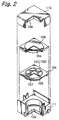
- a conventional lumped element type circulator has an assembled circulator element with a circular plane shape and a basic structure as shown in an exploded oblique view of Fig. 1.
- a reference numeral 100 denotes a circular substrate made of a non-magnetic material such as a glass-reinforced epoxy.
- Center conductors (inner conductors) 101 and 102 are formed on the top face and next to the bottom face of the non-magnetic material substrate 100, respectively. These inner conductors 101 and 102 are electrically connected with each other by via holes 103 passing through the substrate 100.
- Circularly shaped members 104 and 105 made of a ferromagnetic material are attached to the both faces of the non-magnetic material substrate 100 having the inner conductors 101 and 102 so that rotating RF (Radio Frequency) magnetic fluxes are induced in these ferromagnetic members 104 and 105 due to an RF power applied to the inner conductors 101 and 102.
- the conventional circulator element of the circulator has a circular plane shape and is constructed by assembling, namely piling and bonding, the ferromagnetic members 104 and 105 on the both sides of the non-magnetic material substrate 100.
- the circulator as a whole is constructed, as shown in its exploded oblique view of Fig. 2, by stacking and fixing in sequence the ferromagnetic members 104 and 105, grounding conductor electrodes 106 and 107, exiting permanent magnets 108 and 109 and a metal housing separated to upper and lower parts 110 and 111 on the both side of the non-magnetic material substrate 100 having the inner conductors 101 (102), respectively.
- the housing parts 110 and 111 form a magnetic path of the magnetic flux from and to the exiting permanent magnets 108 and 109.
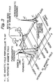
- RF magnetic flux rotating around the inner conductors 101 and 102 will be produced in the ferromagnetic members 104 and 105.
- a dc magnetic field perpendicular to the RF magnetic flux is applied from the permanent magnets 108 and 109, the ferromagnetic members 104 and 105 present different permeability ⁇ + and ⁇ - depending upon rotating sense of the RF magnetic flux, as shown in Fig. 3.
- a circulator utilizes this difference of the permeability depending upon the rotating sense. Namely, a propagation velocity of the RF signal in the circulator element will differ in accordance with the rotating sense and thus the signals transmitting to the opposite directions will be canceled each other resulting that the propagation of the signal to a particular port is prevented.
- a non-propagating port is determined in accordance with its angle against a driving port due to the permeability ⁇ + and ⁇ - of the ferromagnetic member. For example, if ports A, B and C are arranged in this order along a certain rotating sense, the port B will be determined as the non-propagating port against the driving port A and the port C will be determined as the non-propagating port against the driving port B. Terminating one port of thus arranged circulator might constitute an isolator. Termination of the port can be realized by connecting to the port a matched resistor such as a chip resistor, or a thick or thin film resistor formed on a substrate for providing a resonance capacitor.
- a matched resistor such as a chip resistor, or a thick or thin film resistor formed on a substrate for providing a resonance capacitor.
- the ratio of volume occupied by the permanent magnet(s) is typically larger than that of another components. This has made difficult to downsize the non-reciprocal circuit element.
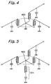
- the serial resonance circuit for adjusting eigen values of in-phase excitation by additionally inserting the serial resonance circuit for adjusting eigen values of in-phase excitation, the relationship of angular difference of 120 degrees in the admittances can be kept for a long time resulting the operation frequency band of the circulator to widen.
- the addition of the LC serial resonance circuit results of increase in the number of components of the circulator and therefore invites difficulty of downsizing of the circulator.
- the LC serial resonance circuit to be added will become large in size.
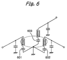
- Japanese Patent Publication No.49(1984)-28219 discloses a circulator with capacitors each of which is inserted between one end of each inner conductor and the grounded conductor.
- An equivalent circuit of this circulator is shown in Fig. 6.
- capacitors 601, 602 and 603 are connected to respective ends of three inner conductors.
- these capacitors will exert an influence upon not only eigen values of in-phase excitation but also eigen values of both positive and negative phase excitations. Therefore, as well as the conventional art shown in Fig. 4, when the frequency changes greatly, it is impossible to keep the relationship of angular difference of 120 degrees in the admittances causing that circulator operation cannot be expected. As a result, the operation frequency band of the circulator is limited to a narrower band.
- a non-reciprocal circuit element such as a circulator.
- the main factor is temperature characteristics of saturation magnetization in the ferromagnetic material such as YIG (yttrium iron garnet) used for the circulator element, or the temperature characteristics of the permanent magnet(s) for providing bias magnetic field.
- change in the temperature characteristics of the ferromagnetic material such as YIG used is larger than that of the bias magnetic field.
- the higher in temperature of the circulator the higher in its operation frequency. This causes effective frequency band to be used to become narrower.
- gadolinium is substituted in YIG to improve the temperature characteristics of saturation magnetization in YIG.
- the substitution of gadolinium causes loss of YIG to increase and therefore invites increased insertion loss of the circulator. Also, such substitution cannot perfectly adjust the temperature characteristics.
- the non-reciprocal circuit elements themselves are requested to be manufactured in smaller size, in lighter weight and in lower height.
- the conventional art has another problem that if the non-reciprocal circuit element is made in smaller size, its operation frequency will increase and thus it is difficult to obtain a desired operation frequency.
- Another object of the present invention is to provide a non-reciprocal circuit element that can be fabricated without changing material used and can optionally adjust temperature characteristics without inviting increased insertion loss.
- a non-reciprocal circuit element includes a capacitor connected between a shield conductor and a ground of the non-reciprocal circuit element, for adjusting only eigen values of in-phase excitation.
- a non-reciprocal circuit element includes a plurality of inner conductors intersecting with keeping insulation with each other, a shield conductor connected in common to one ends of the inner conductors, and a capacitor connected between the shield conductor and an ground of the non-reciprocal circuit element, for adjusting only eigen values of in-phase excitation.
- both center frequency of isolation and applied bias magnetic field can be simultaneously decreased.
- a smaller sized circulator element can be used.
- a non-reciprocal circuit element with smaller size, lighter weight and lower height can be realized.
- a smaller sized permanent magnet can be used, resulting further downsizing of the non-reciprocal circuit element to realize.
- downsizing of the non-reciprocal circuit element will be expedited.
- Selecting the capacitance value of this additional capacitor can optionally change the amount of frequency change per unit of magnetic field dF/dH. If dF/dH increases, the temperature characteristics of the non-reciprocal circuit element is affected more strongly by the temperature characteristics of the bias magnetic field and thus there occurs an effect as if the temperature characteristics of the bias magnetic field increases. As a result, the temperature characteristics of the circulator can be improved.
- the dF/dH can be optionally changed depending upon the capacitance value of the additional capacitor. Thus, the temperature characteristics of the circulator can be optionally adjusted by selecting the capacitance value. If the capacitance value is determined to an optimum value, a circulator with substantially constant temperature characteristics may be realized.
- the additional capacitor is a capacitor with a capacitance value of Cs [pF] which satisfies Cs ⁇ C ⁇ 1500 , where C [pF] is a parallel resonance capacitance value of the non-reciprocal circuit element. More preferably, the additional capacitor is a capacitor with a capacitance value of Cs [pF] which satisfies Cs ⁇ C ⁇ 900 .
- the inner conductors are strip lines folded on the ferromagnetic material body.
- the additional capacitor preferably includes the shield conductor, the ground and a resin material that is inserted between the shield conductor and the ground as a dielectric material.
- the inner conductors are conductors formed integrally in the ferromagnetic material body.
- the additional capacitor preferably includes the shield conductor, the ground and a ceramic material that is inserted between the shield conductor and the ground as a dielectric material.
- the additional capacitor is a capacitor formed integrally with the ferromagnetic material body.
- input/output capacitors are formed between input/output ports and the ground, or between input/output ports and the shield conductor.
- a lumped element type isolator as a preferred embodiment of a non-reciprocal circuit element according to the present invention will be described.
- this embodiment is in a case of the lumped element type isolator, the present invention can be applied to a distributed element type isolator, a lumped element type circulator and a distributed element type circulator.
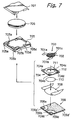
- Fig. 7 is an exploded oblique view schematically illustrating whole configuration and assembling order of the lumped element type isolator as a preferred embodiment of a non-reciprocal circuit element according to the present invention
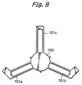
- Fig. 8 is a plane view illustrating expanded state before folding with respect to inner conductors and a shield conductor of the embodiment shown in Fig. 7
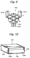
- Fig. 9 is a plane view illustrating an assembly constituted by folding the inner conductors of the embodiment shown in Fig. 7 on a ferrite core
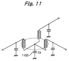
- Fig. 10 is an oblique view illustrating the assembled lumped element type isolator of the embodiment shown in Fig. 7.
- reference numeral 700 denotes a shield conductor (shield plate), 701a, 701b and 701c denote strip lines which constitute the three inner conductors, and 702 denotes the circular plate shaped ferrite core made of YIG, respectively.
- the shield conductor 700 and the strip lines 701a, 701b and 701c are formed by stamping of a copper foil, as shown in Fig. 8, so that the three strip lines 701a, 701b and 701c are elongated and protruded from the shield conductor 700 in radial directions.
- the end portions of the strip lines 701a and 701b are used as input/output terminals and the end portion of the strip line 701c is terminated.
- the shield conductor 700 is formed in a circular shape with substantially the same size as that of the ferrite core 702 disposed thereon.
- the assembly 703 consisting of the strip lines as for the three inner conductors and the circular ferrite core is formed as follows. First, the circular ferrite core 702 is disposed on the shield conductor 700. Thereafter, one of strip lines 701a and 701b with the input/output terminals is folded along the peripheral edge of the ferrite core 702, and then the other one is also folded. Finally, the strip line 701c with the terminal to be connected to a terminating resistance along the peripheral edge of the ferrite core 702. Thus, as shown in Figs. 7 and 9, the assembly 703 with three strip lines 701a, 701b and 701c folded on the upper face of the circular ferrite core 702 to cross with each other is formed.
- strip lines 701a, 701b and 701c are folded on the circular ferrite core 702
- insulating sheets made of polyimide material are inserted between the strip lines 701a, 701b and 701c to make electrical insulation among them.
- the lumped element type isolator has, other than the assembly 703, an inner substrate 704 with the terminating resistor and necessary capacitors, a resin housing 705 shaped in a rectangular frame, a permanent magnet 706 for applying DC magnetic field to the assembly 703 in the thickness direction of the ferrite core 702, upper and lower covers 707 and 708 attached in integral to the resin housing 705 to cover upper and lower sides of the housing 705, which operate as soft magnetic yokes, a terminal substrate 709 used for plane-mounting, and an insulating sheet 710 for forming an additional capacitor (capacitance value of Cs) according to the present invention, which will adjust only eigen values of in-phase excitation.
- an additional capacitor capacitor
- the dielectric insulating sheet 710 is inserted between the assembly 703 and the lower cover 708 so as to form the additional capacitor with the capacitance value Cs, in which the shield conductor 700 of the assembly 703 and the under cover 708 operate as capacitor electrodes.
- the insulating sheet 710 can be made of any dielectric material other than resin material such as polyimide.
- the inner substrate 704 made of dielectric material has a through hole 711 at its center portion for holding the assembly 703 inserted therein.
- capacitor electrodes 704a, 704b and 704c with predetermined shapes, to which the end portions of the strip lines 701a, 701b and 701c are electrically connected, and a shield electrode 704d are formed.
- a terminating resistor 712 made of for example ruthenium oxide is formed by a thick-film printing. The terminating resistor 712 is connected between the capacitor electrode 704c connected with the end portion of the strip line 701c and the shield electrode 704d.
- a ground electrode that forms input/output capacitors between it and the capacitor electrodes 704a, 704b and 704c is formed. This ground electrode is directly grounded.
- the assembly 703 is fitted in the hole 711 of the substrate 704 and then the end portions of the strip lines 701a, 701b and 701c are electrically connected to the capacitor electrodes 704a, 704b and 704c on the substrate 704, respectively.
- the inner substrate 704 with the fitted assembly 703 is disposed on the lower cover 708 made of soft magnetic metal material such as iron via the insulating sheet 710.
- the rectangular frame shaped housing 705 has two connection electrodes 705a and 705b at positions corresponding to the end portions or input/output terminals of the two strip lines 701a and 701b, respectively.
- the housing 705 also has a ground connection electrode 705d for grounding one end of the terminating resistor 712, at a position of the ground electrode 704d.
- the under cover 708 with the assembly 703 attached thereto is assembled. Soldering to the inner end portions of the connection electrodes 705a and 705b respectively connects the end portions of the strip lines 701a and 701b and also the capacitor electrodes 704a and 704b. Soldering to the inner end portion of the ground connection electrode 705d connects the ground electrode 704d.
- the permanent magnet 706 is fixed in the upper cover 707 made of soft magnetic metal material such as iron.
- the upper cover 707 containing the permanent magnet 706 is assembled on the resin housing 705, and the upper cover 707 and the lower cover 708 are caulked with each other to make them in one piece.
- the permanent magnet 706 and the ferrite core 702 with the strip lines 701a, 701b and 701c formed thereon are arranged inside and surrounded by a magnetic yoke constituted by these upper and lower covers 707 and 708.
- the terminal substrate 709 has next to its bottom face two plane-mounting terminal electrodes 709a and 709b used for connection with external circuits at positions corresponding to the input/output terminal end portions of the two strip lines 701a and 701b, and a ground electrode 709d.
- the terminal substrate 709 also has on its top face electrodes 709a' and 709b' which are respectively connected to the plane-mounting terminal electrodes 709a and 709b through via holes (not shown), and an electrodes 709d' which is connected to the ground electrode 709d through a via hole (not shown).
- This terminal substrate 709 is mounted next to the bottom face of the under cover 708.
- the electrodes 709a' and 709b' are connected by soldering to the outer end portions of the connection electrodes 705a and 705b of the resin housing 705, respectively.
- the electrode 709d' is connected by soldering to the bottom face of the under cover 708.
- the lumped element type isolator in which the input/output terminal end portions of the two strip lines 701a and 701b are electrically connected to the plane-mounting terminal electrodes 709a and 709b of the terminal substrate 709, and the end portion of the strip line 701c is terminated by being connected to the ground electrode 709d through the terminating resistor 712 is provided.
- a plurality of samples with the same structure as the above-mentioned lumped element type isolator but with different values of Cs ⁇ C were fabricated.
- the size of the circular ferrite core 702 is 3.5 mm in diameter and 0.4 mm in thickness.
- center frequency of isolation center frequency of isolation
- relative intensity of applied bias magnetic field changed amount of center frequency of isolation when the temperature varies from -25 °C to +85 °C were measured, respectively.
- the measured results are indicated in Table 1.
- FIG. 11 An equivalent circuit of the non-reciprocal circuit element or the circulator in this embodiment is shown in Fig. 11 in comparison with that of the conventional circulator shown in Fig. 4.
- one ends of the three inner conductors which consist three inductors are connected together and a capacitor 1100 with a capacitance value Cs for adjusting the eigen values of in-phase excitation is additionally connected between the connected ends of the three inner conductors and the ground.
- the non-grounded electrode of the capacitance 1100 shown in Fig. 11 corresponds to the shield conductor 700.
- the capacitance value Cs acts only the admittance of in-phase excitation and represented as follows.
- y 1 j ⁇ C-j 1 ⁇ L 1 - 3 ⁇ Cs
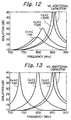
- Fig. 12 shows calculation results of isolation characteristics when a capacitance value Cs of the additional capacitor 1100 is varied.
- Fig. 13 shows calculation results of adjusted isolation characteristics when the applied magnetic field is reduced so that the maximum isolation value of each case becomes its largest value. As will be noted from this figure, by reducing the applied magnetic field, the center frequency of the isolation more lowers.
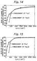
- Fig. 14 shows relationship between Cs ⁇ C and the center frequency of isolation and Fig. 15 shows relationship between Cs ⁇ C and applied magnetic field.
- FIG. 14 shows relationship between Cs ⁇ C and the center frequency of isolation and Fig. 15 shows relationship between Cs ⁇ C and applied magnetic field.
- the operation frequency will greatly lower when Cs ⁇ C ⁇ 1500 [(pF) 2 ] .
- a desired range of Cs ⁇ C will be equal to or less than 1500 [(pF) 2 ].
- the applied magnetic field will greatly lower when Cs ⁇ C ⁇ 900 [(pF) 2 ] .
- a more desired range of Cs ⁇ C will be equal to or less than 900 [(pF) 2 ].
- size of the circulator element is inversely proportional to its operation frequency. Namely, if the operation frequency decreases, a smaller sized circulator element can be used and therefore downsizing of overall circulator can be expected. In addition, since a smaller sized permanent magnet can be used when the applied magnetic field decreases, the circulator can be further downsized.
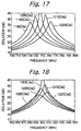
- Fig. 16 shows a relationship between Cs ⁇ C and amount of frequency change per unit magnetic field dF/dH as a result of calculation of the frequency change when the applied magnetic field and also Cs ⁇ C are varied.
- dF/dH becomes larger than that when no capacitor is added.
- the smaller capacitance value Cs will result the larger dF/dH (the amount of change in frequency with respect to the amount of change in applied magnetic field).
- the dF/dH can be optionally changed by appropriately selecting the value of Cs.
- a non-reciprocal circuit element such as a circulator
- Two main factors are temperature characteristics of magnetization saturation of the ferromagnetic material such as YIG, utilized in a circuit element and temperature characteristics of the permanent magnet for providing bias magnetic field.
- the operation frequency of the conventional circulator will increase when the temperature rises causing the available frequency band to limit in fact.
- dF/dH increases by adding the capacitor 1100 with the capacitance value Cs as aforementioned. This means that the temperature characteristics of the circulator is affected more strongly by the temperature characteristics of the bias magnetic field. In other words, according to the present invention, since there occurs an effect as if the temperature characteristics of the bias magnetic field increases, the temperature characteristics of the circulator can be improved.
- the dF/dH can be optionally changed depending upon the capacitance value Cs.
- the temperature characteristics of the circulator can be optionally adjusted by selecting the capacitance value Cs. If the value Cs is determined to an optimum value, a circulator with substantially constant temperature characteristics may be realized.
- Fig. 19 is an oblique view schematically illustrating configuration of a circulator element part of a lumped element type isolator as another embodiment of a non-reciprocal circuit element according to the present invention
- Fig. 20 is an A-A sectional view of Fig. 19
- Fig. 21 is an exploded oblique view schematically illustrating whole configuration of the embodiment shown in Fig. 19.
- this embodiment is in a case of the lumped element type isolator, the present invention can be applied to a distributed element type isolator, a lumped element type circulator and a distributed element type circulator.
- reference numeral 1900 denotes a circulator element formed by integrating and sintering ferromagnetic material body and inner conductors (center conductors) 1901 with a trigonally symmetric pattern
- 1902 denotes a shield conductor formed next to whole bottom face and on a part of the side faces of the circulator element 1900
- 1903a, 1903b and 1903c denote terminal electrodes formed on the side faces of the circulator element 1900 and connected to one ends of the respective inner conductors 1901
- 1904 denotes an inner substrate
- 1905 denotes an exciting permanent magnet
- 1906 denotes a yoke made of soft magnetic metal such as iron
- 1907 denotes a dielectric material layer formed next to the bottom face of the shield conductor 1902 for forming an additional capacitor (capacitance value of Cs) according to the present invention, which will adjust only eigen values of in-phase excitation, respectively.
- the dielectric material layer 1907 is inserted between the shield conductor 1902 and one face of the yoke 1906 located under the conductor 1902 so as to form the additional capacitor with the capacitance value Cs, in which the shield conductor 1902 of the circulator element 1900 and the one face of the yoke 1906 operate as capacitor electrodes.
- the dielectric material layer 1907 can be made of any dielectric material other than ceramics.
- the inner substrate 1904 made of dielectric material has a through hole 1908 at its center portion for holding the circulator element 1900 inserted therein.
- capacitor electrodes 1904a, 1904b and 1904c with predetermined shapes, to which the terminal electrodes 1903a, 1903b and 1903c of the circulator element 1900 are electrically connected, respectively are formed on the top face of the substrate 1904.
- a terminating resistor 1909 made of for example ruthenium oxide is formed by a thick-film printing. The terminating resistor 1909 is connected between the capacitor electrode 1904c connected with the terminal electrode 1903c and a ground electrode 1904d.
- a ground electrode that forms input/output capacitors between it and the capacitor electrodes 1904a, 1904b and 1904c is formed next to the whole bottom face of the substrate 1904.
- the capacitor electrodes 1904a and 1904b also constitute an input terminal and an output terminal, and the ground electrode 1904d also constitutes a ground terminal.
- yttrium oxide (Y 2 O 3 ) material powder and iron oxide material (Fe 2 O 3 ) powder are mixed together in a molar ratio of 3 : 5, and then the mixed powder is calcinated at 1200 °C.
- ferromagnetic material slurry is formed into green sheets by using a doctor blade.
- via holes are formed in the green sheet by means of a punching machine.
- a pattern of the inner conductors 1901 is formed by a conductive material by using a thick-film printing, and simultaneously the via holes are filled by the conductive material.
- the conductive material used may be silver paste for example.
- the green sheets with thus formed inner conductors and via holes are stacked with each other and then the stacked sheets are hot-pressed. And then, the hot-pressed sheets are diced and separated into discrete circulator elements. The separated elements are then sintered at 1480 °C. Baking silver paste next to the whole bottom face of the sintered element forms the shield conductor 1902.
- the terminal electrodes 1903a, 1903b and 1903c, and connection electrodes for connecting the other ends of the inner conductors with the shield conductor 1902 are also formed by baking silver paste on the side faces of the sintered element. As a result, the circulator element 1900 is completed.
- the dielectric material layer 1907 is formed by printing ceramic paste on the face of the shield conductor 1902 of the circulator element 1900 and by firing them.
- a lumped element type isolator can be fabricated by assembling the inner substrate 1904, the permanent magnet 1905 and the upper and lower yoke 1906 with thus obtained circulator element 1900 as shown in Fig. 21.
- An additional capacitor with a capacitance value Cs is formed by the shield conductor 1902 and one face of the yoke 1906 between which the dielectric material layer 1907 made of ceramic material is sandwiched.
- the value of Cs ⁇ C of this isolator was 50 [(pF) 2 ].
- center frequency of isolation center frequency of isolation
- relative intensity of applied bias magnetic field changed amount of center frequency of isolation when the temperature varies from -25 °C to +85 °C were measured, respectively.
- the measured results are indicated in Table 3.
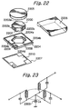
- Fig. 22 is an oblique view schematically illustrating configuration of a circulator element part of a lumped element type isolator as a further embodiment of a non-reciprocal circuit element according to the present invention.
- this embodiment is in a case of the lumped element type isolator, the present invention can be applied to a distributed element type isolator, a lumped element type circulator and a distributed element type circulator.
- reference numeral 2200 denotes a circulator element formed by integrating and sintering ferromagnetic material body and inner conductors (center conductors) with a trigonally symmetric pattern
- 2202 denotes a shield conductor formed next to whole bottom face and on a part of the side faces of the circulator element 2200
- 2203a, 2203b and 2203c denote terminal electrodes formed on the side faces of the circulator element 2200 and connected to one ends of the respective inner conductors
- 2204 denotes an inner substrate
- 2205 denotes an exciting permanent magnet
- 2206 denotes a yoke made of soft magnetic metal such as iron
- 2207 denotes a dielectric material layer formed next to the bottom face of the shield conductor 2202 for forming an additional capacitor (capacitance value of Cs) according to the present invention, which will adjust only eigen values of in-phase excitation
- 2210 denotes another shield conductor, respectively.
- the another shield conductor 2210 is inserted between the shield conductor 2202 formed next to the bottom face of the circulator element 2200 and a shield electrode (not shown) formed next to the bottom face of the inner substrate 2204 so as to connect with the shield conductor 2202 and the shield electrode.
- the dielectric material layer 2207 is inserted between the another shield conductor 2210 and one face of the yoke 2206 located under the conductor 2210 so as to form the additional capacitor with the capacitance value Cs, in which the another shield conductor 2210 and the one face of the yoke 2206 operate as capacitor electrodes.
- the dielectric material layer 2207 can be made of any dielectric material other than ceramics.
- the inner substrate 2204 made of dielectric material has a through hole 2208 at its center portion for holding the circulator element 2200 inserted therein.
- capacitor electrodes 2204a, 2204b and 2204c with predetermined shapes, to which the terminal electrodes 2203a, 2203b and 2203c of the circulator element 2200 are electrically connected, respectively are formed.
- a terminating resistor 2209 made of for example ruthenium oxide is formed by a thick-film printing. The terminating resistor 2209 is connected between the capacitor electrode 2204c connected with the terminal electrode 2203c and a ground electrode 2204d.
- a shield electrode that forms input/output capacitors between it and the capacitor electrodes 2204a, 2204b and 2204c is formed next to the whole bottom face of the substrate 2204.
- the capacitor electrodes 2204a and 2204b also constitute an input terminal and an output terminal
- the ground electrode 2204d also constitutes a ground terminal.
- yttrium oxide (Y 2 O 3 ) material powder and iron oxide material (Fe 2 O 3 ) powder are mixed together in a molar ratio of 3 : 5, and then the mixed powder is calcinated at 1200 °C.
- ferromagnetic material slurry is formed into green sheets by using a doctor blade.
- via holes are formed in the green sheet by means of a punching machine.
- a pattern of the inner conductors is formed by a conductive material by using a thick-film printing, and simultaneously the via holes are filled by the conductive material.
- the conductive material used may be silver paste for example.
- the green sheets with thus formed inner conductors and via holes are stacked with each other and then the stacked sheets are hot-pressed. And then, the hot-pressed sheets are diced and separated into discrete circulator elements. The separated elements are then sintered at 1480 °C. Baking silver paste next to the whole bottom face of the sintered element forms the shield conductor 2202.
- the terminal electrodes 2203a, 2203b and 2203c, and connection electrodes for connecting the other ends of the inner conductors with the shield conductor 2202 are also formed by baking silver paste on the side faces of the sintered element. As a result, the circulator element 2200 is completed.
- fabricated circulator element 2200 is attached to the inner substrate 2204, and then the another shield conductor 2210 which is connected to the whole shield electrode and to the shield electrode formed next to the bottom face of the inner substrate 2204 and the dielectric material layer 2207 is stacked in this order. Thereafter, by assembling the permanent magnet 2205 and the upper and lower yoke 2206 with them as shown in Fig. 22, a lumped element type isolator can be fabricated.
- An additional capacitor with a capacitance value Cs is formed by the shield conductor 2210 and one face of the yoke 2206 between which the dielectric material layer 2207 made of ceramic material is sandwiched.
- Fig. 23 shows an equivalent circuit diagram of the non-reciprocal circuit element (isolator) of this embodiment shown in Fig. 22.
- a capacitor 2300 with a capacitance value Cs for adjusting the eigen values of in-phase excitation is additionally connected between the connected ends of the three inner conductors and the ground.
- one electrode of the input/output capacitors are not directly grounded but connected to the another shield conductor 2210, and therefore one electrodes of the input/output capacitors are grounded via the additional capacitor 2300.
- Ungrounded electrode of the additional capacitor 2300 shown in Fig. 23 corresponds to the another shield conductor 2210 and the above-mentioned one electrode connected thereto.
- both the operation frequency of the circulator and the magnetic field to be applied thereto can be lowered.
- the operation frequency will greatly lower when Cs ⁇ C ⁇ 1500 [(pF) 2 ] .
- a desired range of Cs ⁇ C will be equal to or less than 1500 [(pF) 2 ].
- the applied magnetic field will greatly lower when Cs ⁇ C ⁇ 900 [(pF) 2 ] .
- a more desired range of Cs ⁇ C will be equal to or less than 900 [(pF) 2 ].
- Addition of the capacitor with the capacitance value Cs will present not only lowering of center frequency of isolation and lowering of applied bias magnetic field but also improvement of temperature characteristics of the lumped element type isolator as well as in the previous embodiment.
- both center frequency of isolation and applied bias magnetic field can be simultaneously decreased.
- a smaller sized circulator element can be used.
- a non-reciprocal circuit element with smaller size, lighter weight and lower height can be realized.
- a smaller sized permanent magnet can be used, resulting further downsizing of the non-reciprocal circuit element to realize.
- downsizing of the non-reciprocal circuit element will be expedited.
- Selecting the capacitance value of this additional capacitor can optionally change the amount of frequency change per unit of magnetic field dF/dH. If dF/dH increases, the temperature characteristics of the non-reciprocal circuit element are affected more strongly by the temperature characteristics of the bias magnetic field and thus there occurs an effect as if the temperature characteristics of the bias magnetic field increase. As a result, the temperature characteristics of the circulator can be improved.
- the dF/dH can be optionally changed depending upon the capacitance value of the additional capacitor.
- the temperature characteristics of the circulator can be optionally adjusted by selecting the capacitance value. If the capacitance value is determined to an optimum value, a circulator with substantially constant temperature characteristics may be realized. In other words, temperature characteristics can be optionally adjusted without changing material used and without inviting increased insertion loss.
Landscapes
- Non-Reversible Transmitting Devices (AREA)
Applications Claiming Priority (5)
| Application Number | Priority Date | Filing Date | Title |
|---|---|---|---|
| JP35201197 | 1997-12-08 | ||
| JP35201197 | 1997-12-08 | ||
| JP2407998 | 1998-01-22 | ||
| JP02407998A JP3807071B2 (ja) | 1997-12-08 | 1998-01-22 | 非可逆回路素子 |
| PCT/JP1998/005103 WO1999030382A1 (en) | 1997-12-08 | 1998-11-13 | Irreversible circuit element |
Publications (2)
| Publication Number | Publication Date |
|---|---|
| EP0959520A1 true EP0959520A1 (de) | 1999-11-24 |
| EP0959520A4 EP0959520A4 (de) | 2002-07-31 |
Family
ID=26361567
Family Applications (1)
| Application Number | Title | Priority Date | Filing Date |
|---|---|---|---|
| EP98953033A Withdrawn EP0959520A4 (de) | 1997-12-08 | 1998-11-13 | Irreversibles schaltungselement |
Country Status (5)
| Country | Link |
|---|---|
| US (1) | US6215371B1 (de) |
| EP (1) | EP0959520A4 (de) |
| JP (1) | JP3807071B2 (de) |
| CN (1) | CN1174519C (de) |
| WO (1) | WO1999030382A1 (de) |
Cited By (1)
| Publication number | Priority date | Publication date | Assignee | Title |
|---|---|---|---|---|
| EP2093827A1 (de) * | 2008-02-20 | 2009-08-26 | NTT DoCoMo, Inc. | Nichtreziprokes Schaltungselement |
Families Citing this family (17)
| Publication number | Priority date | Publication date | Assignee | Title |
|---|---|---|---|---|
| JP3438683B2 (ja) * | 1999-11-30 | 2003-08-18 | 株式会社村田製作所 | 非可逆回路素子、通信装置および非可逆回路素子の製造方法 |
| US6906597B2 (en) * | 2001-10-29 | 2005-06-14 | Hitachi Metals, Ltd. | Non-reciprocal circuit device and resin casing used therefor |
| JP3686884B2 (ja) * | 2002-06-06 | 2005-08-24 | アルプス電気株式会社 | 電子部品用筐体の製造方法 |
| JP3705253B2 (ja) * | 2002-08-14 | 2005-10-12 | 株式会社村田製作所 | 3ポート型非可逆回路素子および通信装置 |
| US7113065B2 (en) * | 2003-09-30 | 2006-09-26 | Rockwell Automation Technologies, Inc. | Modular inductor for use in power electronic circuits |
| JP4724152B2 (ja) * | 2006-08-31 | 2011-07-13 | 株式会社エヌ・ティ・ティ・ドコモ | 非可逆回路素子 |
| WO2013168771A1 (ja) * | 2012-05-09 | 2013-11-14 | 株式会社村田製作所 | 非可逆回路素子 |
| JP5655990B2 (ja) * | 2012-07-02 | 2015-01-21 | 株式会社村田製作所 | 非可逆回路素子 |
| WO2015037693A1 (ja) * | 2013-09-13 | 2015-03-19 | 株式会社村田製作所 | 非可逆回路素子 |
| WO2015079792A1 (ja) * | 2013-11-29 | 2015-06-04 | 株式会社村田製作所 | 非可逆回路素子 |
| CN104184457A (zh) * | 2014-09-02 | 2014-12-03 | 王少夫 | 一种环行器 |
| JP6592893B2 (ja) * | 2014-12-26 | 2019-10-23 | 日産自動車株式会社 | 電源装置 |
| CN104701594A (zh) * | 2015-03-29 | 2015-06-10 | 王少夫 | 一种环行器装置 |
| CN112838344A (zh) * | 2020-12-31 | 2021-05-25 | 广东大普通信技术有限公司 | 一种环形器 |
| CN116073099A (zh) | 2021-10-29 | 2023-05-05 | Tdk株式会社 | 不可逆电路元件和具有该不可逆电路元件的通信装置 |
| CN117276835A (zh) * | 2023-09-22 | 2023-12-22 | 电子科技大学 | 铁氧体基板及制备方法 |
| CN119133807B (zh) * | 2024-10-23 | 2025-03-21 | 南京奕可飞电子科技有限公司 | 一种多旋磁组合全屏蔽环行器 |
Family Cites Families (17)
| Publication number | Priority date | Publication date | Assignee | Title |
|---|---|---|---|---|
| US3517340A (en) * | 1968-12-23 | 1970-06-23 | Bell Telephone Labor Inc | Circulator having conductive post capacitively coupled between first and second transmission line conductors for broadbanding purposes |
| JPS4928219B1 (de) * | 1969-04-28 | 1974-07-24 | ||
| BE758313A (fr) | 1969-11-03 | 1971-04-01 | Western Electric Co | Circulateur propre a fonctionner sur une bande de frequences |
| JPS495547A (de) | 1972-05-04 | 1974-01-18 | ||
| JPS4928219A (de) | 1972-07-10 | 1974-03-13 | ||
| JPS509661A (de) | 1973-05-28 | 1975-01-31 | ||
| US3890582A (en) * | 1973-06-15 | 1975-06-17 | Addington Lab Inc | Floating-ground microwave ferrite isolators |
| US3836874A (en) * | 1973-06-25 | 1974-09-17 | Hitachi Ltd | Lumped element circulator |
| JPS608643B2 (ja) * | 1976-12-24 | 1985-03-05 | 日本電気株式会社 | サーキユレータ |
| FR2418967A1 (fr) * | 1978-03-03 | 1979-09-28 | Lignes Telegraph Telephon | Circulateur a elements localises a circuit d'elargissement de bande reglable |
| JPH0218561Y2 (de) * | 1980-02-19 | 1990-05-24 | ||
| JPS56123624A (en) | 1980-03-05 | 1981-09-28 | Mitsubishi Rayon Co | Polypropylene film for electric article |
| JP2526219B2 (ja) * | 1986-10-23 | 1996-08-21 | 日立フェライト 株式会社 | 集中定数型サ−キユレ−タ及びアイソレ−タ |
| US4920323A (en) * | 1988-12-27 | 1990-04-24 | Raytheon Company | Miniature circulators for monolithic microwave integrated circuits |
| JPH06338707A (ja) | 1993-03-31 | 1994-12-06 | Tdk Corp | サーキュレータ |
| JPH1041706A (ja) * | 1996-07-26 | 1998-02-13 | Hitachi Metals Ltd | 非可逆回路素子 |
| JP3269409B2 (ja) * | 1996-07-26 | 2002-03-25 | 株式会社村田製作所 | 非可逆回路素子 |
-
1998
- 1998-01-22 JP JP02407998A patent/JP3807071B2/ja not_active Expired - Lifetime
- 1998-11-11 US US09/341,672 patent/US6215371B1/en not_active Expired - Lifetime
- 1998-11-13 CN CNB988023504A patent/CN1174519C/zh not_active Expired - Lifetime
- 1998-11-13 WO PCT/JP1998/005103 patent/WO1999030382A1/ja not_active Ceased
- 1998-11-13 EP EP98953033A patent/EP0959520A4/de not_active Withdrawn
Cited By (2)
| Publication number | Priority date | Publication date | Assignee | Title |
|---|---|---|---|---|
| EP2093827A1 (de) * | 2008-02-20 | 2009-08-26 | NTT DoCoMo, Inc. | Nichtreziprokes Schaltungselement |
| US7978018B2 (en) | 2008-02-20 | 2011-07-12 | Ntt Docomo, Inc. | Non-reciprocal circuit device |
Also Published As
| Publication number | Publication date |
|---|---|
| WO1999030382A1 (en) | 1999-06-17 |
| CN1174519C (zh) | 2004-11-03 |
| EP0959520A4 (de) | 2002-07-31 |
| JP3807071B2 (ja) | 2006-08-09 |
| US6215371B1 (en) | 2001-04-10 |
| CN1246966A (zh) | 2000-03-08 |
| JPH11234003A (ja) | 1999-08-27 |
Similar Documents
| Publication | Publication Date | Title |
|---|---|---|
| EP0959520A1 (de) | Irreversibles schaltungselement | |
| EP1098386B1 (de) | Nichtreziproke anordnung mit konzentrierten elementen | |
| EP1939973B1 (de) | Irreversibles schaltelement, herstellungsverfahren dafür und kommunikationsvorrichtung | |
| US7253697B2 (en) | Two-port isolator and communication apparatus | |
| EP0776060B1 (de) | Nichtreziprokes Schaltungselement | |
| US5017894A (en) | Lumped constant non-reciprocal circuit element | |
| US6236285B1 (en) | Lumped element circulator having a plurality of separated operation bands | |
| EP0675561B1 (de) | Herstellungsverfahren eines Mikrowellenzirkulators | |
| CN104272524A (zh) | 不可逆电路元件 | |
| JP4793350B2 (ja) | 2ポート型非可逆回路素子 | |
| US6940360B2 (en) | Two-port isolator and method for evaluating it | |
| US20010030584A1 (en) | Nonreciprocal circuit device and high-frequency circuit apparatus | |
| US6894578B1 (en) | Irreversible circuit module including a directional coupler | |
| EP0682380B1 (de) | Nichtreziprokes Schaltungselement | |
| US6642831B2 (en) | Nonreciprocal circuit device and communication device using same | |
| US6982608B2 (en) | Isolator suitable for miniaturization | |
| JP4947289B2 (ja) | 非可逆回路素子 | |
| US7429901B2 (en) | Non-reciprocal circuit element, composite electronic component, and communication apparatus | |
| JP4423619B2 (ja) | 非可逆回路素子 | |
| US6597253B2 (en) | Nonreciprocal circuit device and communication apparatus including the same | |
| JP3891437B2 (ja) | 3端子対非可逆素子及びこれを用いた通信装置 | |
| JPH1197911A (ja) | 集中定数型非可逆回路素子 | |
| JP3267010B2 (ja) | 非可逆回路素子 | |
| JP2003124710A (ja) | 非可逆回路モジュール | |
| JP2005167581A (ja) | 非可逆回路素子及び通信機装置 |
Legal Events
| Date | Code | Title | Description |
|---|---|---|---|
| PUAI | Public reference made under article 153(3) epc to a published international application that has entered the european phase |
Free format text: ORIGINAL CODE: 0009012 |
|
| 17P | Request for examination filed |
Effective date: 19990810 |
|
| AK | Designated contracting states |
Kind code of ref document: A1 Designated state(s): DE FR GB NL |
|
| A4 | Supplementary search report drawn up and despatched |
Effective date: 20020619 |
|
| AK | Designated contracting states |
Kind code of ref document: A4 Designated state(s): DE FR GB NL |
|
| RIC1 | Information provided on ipc code assigned before grant |
Free format text: 7H 01P 1/383 A, 7H 01P 1/36 B, 7H 01P 1/387 B |
|
| 17Q | First examination report despatched |
Effective date: 20050705 |
|
| STAA | Information on the status of an ep patent application or granted ep patent |
Free format text: STATUS: THE APPLICATION IS DEEMED TO BE WITHDRAWN |
|
| 18D | Application deemed to be withdrawn |
Effective date: 20100107 |