EP0959465A2 - Laminierte Scheibe und Verfahren zur Herstellung derselben - Google Patents
Laminierte Scheibe und Verfahren zur Herstellung derselben Download PDFInfo
- Publication number
- EP0959465A2 EP0959465A2 EP98112056A EP98112056A EP0959465A2 EP 0959465 A2 EP0959465 A2 EP 0959465A2 EP 98112056 A EP98112056 A EP 98112056A EP 98112056 A EP98112056 A EP 98112056A EP 0959465 A2 EP0959465 A2 EP 0959465A2
- Authority
- EP
- European Patent Office
- Prior art keywords
- disk
- transparent substrate
- laminating surface
- laminated
- laminating
- Prior art date
- Legal status (The legal status is an assumption and is not a legal conclusion. Google has not performed a legal analysis and makes no representation as to the accuracy of the status listed.)
- Withdrawn
Links
Images

Classifications
-
- G—PHYSICS
- G11—INFORMATION STORAGE
- G11B—INFORMATION STORAGE BASED ON RELATIVE MOVEMENT BETWEEN RECORD CARRIER AND TRANSDUCER
- G11B7/00—Recording or reproducing by optical means, e.g. recording using a thermal beam of optical radiation by modifying optical properties or the physical structure, reproducing using an optical beam at lower power by sensing optical properties; Record carriers therefor
- G11B7/24—Record carriers characterised by shape, structure or physical properties, or by the selection of the material
- G11B7/26—Apparatus or processes specially adapted for the manufacture of record carriers
-
- B—PERFORMING OPERATIONS; TRANSPORTING
- B29—WORKING OF PLASTICS; WORKING OF SUBSTANCES IN A PLASTIC STATE IN GENERAL
- B29C—SHAPING OR JOINING OF PLASTICS; SHAPING OF MATERIAL IN A PLASTIC STATE, NOT OTHERWISE PROVIDED FOR; AFTER-TREATMENT OF THE SHAPED PRODUCTS, e.g. REPAIRING
- B29C65/00—Joining or sealing of preformed parts, e.g. welding of plastics materials; Apparatus therefor
- B29C65/02—Joining or sealing of preformed parts, e.g. welding of plastics materials; Apparatus therefor by heating, with or without pressure
- B29C65/14—Joining or sealing of preformed parts, e.g. welding of plastics materials; Apparatus therefor by heating, with or without pressure using wave energy, i.e. electromagnetic radiation, or particle radiation
- B29C65/1403—Joining or sealing of preformed parts, e.g. welding of plastics materials; Apparatus therefor by heating, with or without pressure using wave energy, i.e. electromagnetic radiation, or particle radiation characterised by the type of electromagnetic or particle radiation
- B29C65/1406—Ultraviolet [UV] radiation
-
- B—PERFORMING OPERATIONS; TRANSPORTING
- B29—WORKING OF PLASTICS; WORKING OF SUBSTANCES IN A PLASTIC STATE IN GENERAL
- B29C—SHAPING OR JOINING OF PLASTICS; SHAPING OF MATERIAL IN A PLASTIC STATE, NOT OTHERWISE PROVIDED FOR; AFTER-TREATMENT OF THE SHAPED PRODUCTS, e.g. REPAIRING
- B29C65/00—Joining or sealing of preformed parts, e.g. welding of plastics materials; Apparatus therefor
- B29C65/48—Joining or sealing of preformed parts, e.g. welding of plastics materials; Apparatus therefor using adhesives, i.e. using supplementary joining material; solvent bonding
- B29C65/4805—Joining or sealing of preformed parts, e.g. welding of plastics materials; Apparatus therefor using adhesives, i.e. using supplementary joining material; solvent bonding characterised by the type of adhesives
- B29C65/483—Reactive adhesives, e.g. chemically curing adhesives
- B29C65/4845—Radiation curing adhesives, e.g. UV light curing adhesives
-
- B—PERFORMING OPERATIONS; TRANSPORTING
- B29—WORKING OF PLASTICS; WORKING OF SUBSTANCES IN A PLASTIC STATE IN GENERAL
- B29C—SHAPING OR JOINING OF PLASTICS; SHAPING OF MATERIAL IN A PLASTIC STATE, NOT OTHERWISE PROVIDED FOR; AFTER-TREATMENT OF THE SHAPED PRODUCTS, e.g. REPAIRING
- B29C66/00—General aspects of processes or apparatus for joining preformed parts
- B29C66/40—General aspects of joining substantially flat articles, e.g. plates, sheets or web-like materials; Making flat seams in tubular or hollow articles; Joining single elements to substantially flat surfaces
- B29C66/41—Joining substantially flat articles ; Making flat seams in tubular or hollow articles
- B29C66/45—Joining of substantially the whole surface of the articles
-
- B—PERFORMING OPERATIONS; TRANSPORTING
- B29—WORKING OF PLASTICS; WORKING OF SUBSTANCES IN A PLASTIC STATE IN GENERAL
- B29L—INDEXING SCHEME ASSOCIATED WITH SUBCLASS B29C, RELATING TO PARTICULAR ARTICLES
- B29L2017/00—Carriers for sound or information
- B29L2017/001—Carriers of records containing fine grooves or impressions, e.g. disc records for needle playback, cylinder records
- B29L2017/003—Records or discs
- B29L2017/005—CD''s, DVD''s
Definitions
- the present invention relates to a two-disk laminated disk for DVD and the like, and also to a method of producing the same.
- energy-radiation setting resin such as ultraviolet setting resin, which is liquid at room temperature, is used as an adhesive, and one side or both sides of the two disks are subjected to energy radiation.
- a transparent disk substrate made of polycarbonate or the like with information pits formed thereon are usually prepared by injection molding.
- a DVD single-sided single layer disk has a reflective film made of aluminum or the like on the surface of the pits on the molded record reading side (hereinafter referred to as "recorded disk") of the disk.
- recorded disk a reflective film made of aluminum or the like on the surface of the pits on the molded record reading side (hereinafter referred to as "recorded disk") of the disk.
- Japanese Patent Application Laid-Open No. 5-20714 discloses a method in which a ultraviolet-setting resin is applied onto the reflective film in a doughnut-like shape, the transparent substrate disk (hereinafter referred to as "dummy disk") is placed on the reflective film, the two laminated disks are rotated so that the resin (adhesive) can be spread all over the disk surface (spinner process), and one side or both sides of the disks are subjected to ultraviolet radiation so as to cure and laminate the disks.
- the ultraviolet-setting resin is liquid before setting, and there is often a problem that air is trapped between the surface of the dummy disk and the ultraviolet-setting resin, when the recorded disk with an aluminum reflective film and a doughnut-like ultraviolet-setting resin applied thereon is laminated on the dummy disk that is a transparent substrate made of polycarbonate. This is because the surface tension between the surface of the dummy disk and the ultraviolet-setting resin is unbalanced, which is to say, the wetting of the resin is poor.
- the resin is not yet spread all over the disk at the time of lamination of the recorded disk and the dummy disk. It is spread just outside the doughnut shape of the previously applied ultraviolet-setting resin.
- the ultraviolet-setting resin is spread all over the disk surface by high speed rotation, and at the same time, extra ultraviolet-setting resin is severed. Even if no air is trapped at the time of the lamination, it may appear at the time of the severing of the ultraviolet-setting resin by rotation.
- Air is more likely to be trapped on the surface of the dummy disk than on the surface of the recorded disk. They tend to appear when the wetting is poor on the polycarbonate surface for the ultraviolet-setting resin.
- Table 1 shows the results of comparisons in the number of disks containing trapped air among 100 laminated disks each having a thin metal film formed on the laminating surface of the dummy disk.
- the substrate (2)(molded product PC1) is used for the laminating surfaces (3) to (6).
- the number of disks with trapped air greatly varies depending on the condition of the surface on the molding side of a mold or a stamper for molding the substrate of the injection molding device.
- the air is trapped on the substrate PC1 due to impurities such as fat and oil in the form of such a thin layer that it cannot be recognized by an ordinary microscope.
- the impurities on the surface of the mold or stamper is transferred onto the disk surface, and at the time of lamination of the substrate and the ultraviolet-setting resin, the transferred impurities flick the ultraviolet-setting resin, causing air to be trapped on the disk surface.
- the trapped air can be seen through the dummy disk that is a transparent substrate, they adversely affect the appearance of the product. Furthermore, the ultraviolet-setting resin contracts more or less at the time of setting, while the trapped air tends to expand due to the temperature rise caused by the ultraviolet radiation. Accordingly, a volume difference is caused between the air-trapped area and non air-trapped area, and as a result, the air-trapped area stands out when being seen from the aluminum surface of the recorded disk side, causing tilt and jitter to the disk.
- Table 1 shows the comparisons among the types of the adhesive laminating surface and the numbers of laminated disks containing trapped air.
- laminating surface of the dummy disk the number of laminated disks with trapped air ultraviolet ray transmission rate (%) (1)
- PC molded product: PCi
- PC molded product: PC2
- PC molded product: PC2
- Al film of 50 nm in thickness 5 0.9
- Au film of 20 nm in thickness 4 23 Si film of 20 nm in thickness 0 9
- An aluminum film of 70 nm in thickness is formed on the laminating surface of the recorded disk.
- Each number of disks containing trapped air indicates the number of laminated disks containing trapped air among every 100 laminated disks.
- the ultraviolet ray transmission rate is calculated from the light emitted by a ultraviolet ray irradiator "UVA-402/1MNSC9-WJ02 (the lamp is UVL-4001M3-N1)" manufactured by Ushio Inc. and the value of the light transmitted through the disks (1) to (6) determined by a ultraviolet ray integrating light meter "UIT-150 (the sensor is UVD-S365)” manufactured by Ushio Inc.
- An object of the present invention is to provide a laminated disk which is prevented from containing trapped air so as to avoid tilt and jitter, and a method of producing the same.
- Another object of the present invention is to provide a laminated disk with no degradation in print color tone and little air trapped, and a method of steadily mass-producing the same.
- the method of producing a laminated disk includes the steps of: forming a reflective film on the laminating surface of a recorded disk; forming a silicon (Si) film or a silicon compound (SiOx, SiNx, SiCx) film on the laminating surface of a transparent substrate; and applying an energy-radiation setting adhesive onto the silicon film or the silicon compound film on the laminating surface of the transparent substrate by a spinner so as to laminate the recorded disk on the transparent substrate.
- the silicon film or the silicon compound film dramatically improves wetting of the transparent substrate, so that a large number of laminated disks including little trapped air can be steadily produced.
- the silicon film formed on the laminating surface of the transparent substrate is 1 to 7 nm in thickness.
- the silicon film dramatically improves the wetting of the energy-radiation setting adhesive, so that a method of producing a laminated disk containing little trapped air can be provided.
- the silicon compound film formed on the laminating surface of the transparent substrate is 1 to 9 nm in thickness.
- the silicon compound film dramatically improves the wetting of the energy-radiation setting adhesive, so that a method of producing a laminated disk with little air trapped can be provided.
- the silicon film formed on the laminating surface of the transparent substrate is 1 to 6 nm in thickness.
- the silicon compound film formed on the laminating surface of the transparent substrate is 1 to 7 nm in thickness.
- the silicon film or the silicon compound film formed on the laminating surface of the transparent substrate is 1 to 5 nm in thickness.
- the silicon film formed on the laminating surface of the transparent substrate is 2 to 5 nm in thickness.
- the silicon compound film formed on the laminating surface of the transparent substrate is 3 to 5 nm in thickness.
- the silicon film formed on the laminating surface of the transparent substrate is 2 to 4 nm in thickness.
- the silicon compound film formed on the laminating surface of the transparent substrate is 3 nm in thickness.
- a laminated disk of the present invention includes: a recorded disk having a reflective film on the laminating surface thereof; a transparent substrate having a silicon film or a silicon compound film on the laminating surface thereof; and an energy-radiation setting adhesive layer interposed between the reflective film on the laminating surface of the recorded disk and the silicon film or the silicon compound film on the laminating surface of the transparent substrate.
- the silicon film formed on the laminating surface of the transparent substrate is 1 to 7 nm in thickness.
- the silicon film dramatically improves the wetting of the energy-radiation setting adhesive, so that a laminated disk including little trapped air can be obtained.
- the silicon compound film formed on the laminating surface of the transparent substrate is 1 to 9 nm in thickness.
- the silicon compound film dramatically improves the wetting of the energy-radiation setting adhesive, so that a laminated disk including little trapped air can be obtained.
- the silicon film formed on the laminating surface of the transparent substrate is 1 to 6 nm in thickness.
- the silicon compound film formed on the laminating surface of the transparent substrate is 1 to 7 nm in thickness.
- the silicon film or the silicon compound film formed on the laminating surface of the transparent substrate is 1 to 5 nm in thickness.
- the silicon film formed on the laminating surface of the transparent substrate is 2 to 5 nm in thickness.
- the silicon compound film formed on the laminating surface of the transparent substrate is 3 to 5 nm in thickness.
- the silicon film formed on the laminating surface of the transparent substrate is 2 to 4 nm in thickness.
- the silicon compound formed on the laminating surface of the transparent substrate is 3 nm in thickness.
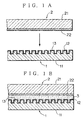
- the reflective film 13 is formed on the pit surface 12 on the laminating surface side of a transparent substrate 11.
- the silicon film or silicon compound film 22 is disposed, by sputtering, on the laminating surface of the transparent substrate 21.
- a ultraviolet-setting adhesive (resin) 3 is applied between the recorded disk 1 and the dummy disk 2 to form a one-sided laminated disk for DVD.
- Fig. 2 is a schematic plan view of a device for producing the laminated disk.
- the DVD one-sided laminated disk producing device 3 comprises a disk feeding position 32, a disk feeding arm 33, a spinner 34, a discharging nozzle 35, a laminated disk transporting arm 36, a UV lamp transporting arm 37 provided with a disk holder 38, a UV lamp 39, a fetching arm 40, and a disk discharging position 31.
- the laminated disk producing device 31 first feeds the recorded disk 1 with the reflective film 13 facing upward to the disk feeding position 32.
- the disk transporting arm 33 then transports the recorded disk 1 from the disk feeding position 32 onto the rotating table of the spinner 34.
- the spinner head of the spinner 34 is lowered.
- the spinner head descends while keeping a distance from the upper surface of the recorded disk 1 by the thickness the dummy disk 2 with the silicon film or silicon compound film 22 formed on the laminating surface on the lower surface.
- the recorded disk 1 transported to the spinner 34 is rotated by a motor (not shown), so that the discharging nozzle 35 applies the ultraviolet-setting adhesive 3 to it.
- the rotation speed is preferably low and in the range of 30 to 100 rpm.
- the dummy disk 2 is then fed to the disk feeding position 32, and the disk feeding arm 33 transports the dummy disk 2 onto the recorded disk 1 with the ultraviolet-setting adhesive 3 applied to it.
- the rotating table is then rotated at a high speed of 2000 to 4000 rpm so that the adhesive between the pair of disks are spread to have a predetermined film thickness.
- the spinner head of the spinner 34 is lifted.
- the laminated disk transporting arm 36 then transports the pair of disks to a lamination station 42 and places them onto the disk holder 38.
- the pair of disks placed on the disk holder 38 are then subjected to ultraviolet radiation by the UV lamp 39 during the transportation by the UV lamp transporting arm 37.
- the ultraviolet-setting adhesive 3 is cured by the ultraviolet radiation.
- the UV lamp transporting arm 37 When the UV lamp transporting arm 37 reaches a transporting position 43, the laminated disks with the cured ultraviolet-setting adhesive 3 are transported to the discharging position 41 by the fetching am 40.
- the laminated disks are fetched from the disk discharging position 41, and the UV lamp transporting am 37 is returned to the lamination station 42, where the UV lamp transporting arm 37 awaits next disks.
- a silicon or silicon compound (SiOx, SiNx, or SiCx) film of a thickness specified later is formed on the laminating surface of the dummy disk 2 by sputtering or the like, before the ultraviolet-setting adhesive 3 is applied to the silicon or silicon compound film on the laminating surface of the dummy disk 2.
- Example 1 Comparative Example 1
- Comparative Example 2 Comparative Example 2
- Comparative Example 3 Comparative Example 3
- Example 1 Comparative Example 3
- Example 4 Example 2
- Example 3 Example 4
- Example 5 Example 6
- Example 7 Example 8
- a silicon or silicon compound (SiOx, SiNx, SiCx) film of 1 to 5 nm in thickness is formed on the laminating surface of the dummy disk by sputtering or the like.
- Another method of producing laminated disks with little trapped air includes the steps of forming a silicon film of 1 to 7 nm in thickness on the laminating surface of the transparent substrate, and then applying the ultraviolet-setting adhesive to the laminating surface of the transparent substrate.
- Yet another method of producing laminated disks with little trapped air includes the steps of forming a silicon compound film of 1 to 9 nm on the laminating surface of the transparent substrate, and then applying the ultraviolet-setting adhesive to the laminating surface of the transparent substrate.
- Still another method of producing laminated disks with little trapped air and little color tone degradation includes the steps of forming a silicon film of 1 to 6 nm in thickness on the laminating surface of the transparent substrate, and then applying the ultraviolet-setting adhesive to the laminating surface of the transparent substrate.
- Another method of producing laminated disks with little trapped air and little color tone degradation includes the steps of forming a silicon compound film of 1 to 7 nm in thickness on the laminating surface of the transparent substrate, and then applying the ultraviolet-setting adhesive to the laminating surface of the transparent substrate.
- Yet another method of producing laminated disks with little trapped air and less color tone degradation includes the steps of forming a silicon film of 2 to 5 nm in thickness on the laminating surface of the transparent substrate, and then applying the ultraviolet-setting adhesive to the laminating surface of the transparent substrate.
- Still another method of producing laminated disks with little trapped air and less color tone degradation includes the steps of forming a silicon compound layer of 3 to 5 nm in thickness on the laminating surface of the transparent substrate, and then applying the ultraviolet-setting adhesive to the laminating surface of the transparent substrate.
- Another method of producing laminated disks with no trapped air and no color tone degradation includes the steps of forming a silicon layer of 2 to 4 nm in thickness on the laminating surface of the transparent, and then applying the ultraviolet-setting adhesive to the laminating surface of the transparent substrate.
- Yet another method of producing laminated disks with no trapped air and no color tone degradation includes the steps of forming a silicon compound layer of 3 nm in thickness on the laminating surface of the transparent substrate, and then applying the ultraviolet-setting adhesive to the laminating surface of the transparent substrate.
- a laminated disk with little trapped air comprises a recorded disk having a reflective film formed on its laminating surface, a transparent substrate having a silicon film of 1 to 7 nm in thickness formed on its laminating surface, and a ultraviolet-setting adhesive layer interposed between the laminating surfaces of the recorded disk and the transparent substrate.
- Another laminated disk with little trapped air comprises a recorded disk having a reflective film formed on its laminating surface, a transparent substrate having a silicon compound film of 1 to 9 nm in thickness formed on its laminating surface, and a ultraviolet-setting adhesive layer interposed between the laminating surfaces of the recorded disk and the transparent substrate.
- Yet another laminated disk with little trapped air and little color tone degradation comprises a recorded disk having a reflective film formed on its laminating surface, a transparent substrate having a silicon film of 1 to 6 nm in thickness formed on its laminating surface, and a ultraviolet-setting adhesive layer interposed between the laminating surfaces of the recorded disk and the transparent substrate.
- Still another laminated disk with little trapped air and little color tone degradation comprises a recorded disk having a reflective film formed on its laminating surface, a transparent substrate having a silicon compound film of 1 to 7 nm in thickness formed on its laminating surface, and a ultraviolet-setting adhesive layer interposed between the laminating surfaces of the recorded disk and the transparent substrate.
- Another laminated disk with little trapped air and less color tone degradation comprises a recorded disk having a reflective film formed on its laminating surface, a transparent substrate having a silicon film of 2 to 5 nm in thickness formed on its laminating surface, and a ultraviolet-setting adhesive layer interposed between the laminating surfaces of the recorded disk and the transparent substrate.
- Yet another laminated disk with little trapped air and less color tone degradation comprises a recorded disk having a reflective surface formed on its laminating surface, a transparent substrate having a silicon compound film of 3 to 5 nm in thickness formed on its laminating surface, and a ultraviolet-setting adhesive layer interposed between the laminating surfaces of the recorded disk and the transparent substrate.
- Still another laminated disk with no trapped air and no color tone degradation comprises a recorded disk having a reflective film formed on its laminating surface, a transparent substrate having a silicon film of 2 to 4 nm in thickness formed on its laminating surface, and a ultraviolet-setting adhesive layer interposed between the laminating surfaces of the recorded disk and the transparent substrate.
- Yet another laminated disk with no trapped air and no color tone degradation comprises a recorded disk having a reflective film formed on its laminating surface, a transparent substrate having a silicon compound film of 3 nm in thickness formed on its laminating surface, and a ultraviolet-setting adhesive layer interposed between the laminating surfaces of the recorded disk and the transparent substrate.
Landscapes
- Engineering & Computer Science (AREA)
- Manufacturing & Machinery (AREA)
- Manufacturing Optical Record Carriers (AREA)
- Lining Or Joining Of Plastics Or The Like (AREA)
- Optical Record Carriers And Manufacture Thereof (AREA)
Applications Claiming Priority (2)
| Application Number | Priority Date | Filing Date | Title |
|---|---|---|---|
| JP13680898A JP3193341B2 (ja) | 1998-05-19 | 1998-05-19 | 貼り合わせディスクおよびその製造方法 |
| JP13680898 | 1998-05-19 |
Publications (2)
| Publication Number | Publication Date |
|---|---|
| EP0959465A2 true EP0959465A2 (de) | 1999-11-24 |
| EP0959465A3 EP0959465A3 (de) | 2000-02-23 |
Family
ID=15183999
Family Applications (1)
| Application Number | Title | Priority Date | Filing Date |
|---|---|---|---|
| EP98112056A Withdrawn EP0959465A3 (de) | 1998-05-19 | 1998-06-30 | Laminierte Scheibe und Verfahren zur Herstellung derselben |
Country Status (2)
| Country | Link |
|---|---|
| EP (1) | EP0959465A3 (de) |
| JP (1) | JP3193341B2 (de) |
Cited By (1)
| Publication number | Priority date | Publication date | Assignee | Title |
|---|---|---|---|---|
| GB2561199A (en) * | 2017-04-04 | 2018-10-10 | Power Roll Ltd | Method |
Family Cites Families (2)
| Publication number | Priority date | Publication date | Assignee | Title |
|---|---|---|---|---|
| NL8702493A (nl) * | 1986-10-31 | 1988-05-16 | Seiko Epson Corp | Optisch opnamemedium en werkwijze voor het vervaardigen daarvan. |
| JPH09259470A (ja) * | 1996-03-21 | 1997-10-03 | Toshiba Corp | 貼合せ情報記録媒体 |
-
1998
- 1998-05-19 JP JP13680898A patent/JP3193341B2/ja not_active Expired - Fee Related
- 1998-06-30 EP EP98112056A patent/EP0959465A3/de not_active Withdrawn
Cited By (2)
| Publication number | Priority date | Publication date | Assignee | Title |
|---|---|---|---|---|
| GB2561199A (en) * | 2017-04-04 | 2018-10-10 | Power Roll Ltd | Method |
| GB2561199B (en) * | 2017-04-04 | 2022-04-20 | Power Roll Ltd | Method |
Also Published As
| Publication number | Publication date |
|---|---|
| JPH11328759A (ja) | 1999-11-30 |
| EP0959465A3 (de) | 2000-02-23 |
| JP3193341B2 (ja) | 2001-07-30 |
Similar Documents
| Publication | Publication Date | Title |
|---|---|---|
| EP1187122A2 (de) | Verfahren und Vorrichtung zur Herstellung eines optischen Informationsaufzeichnungsmediums, und optisches Informationsaufzeichnungsmedium | |
| EP0409663A2 (de) | Optische Scheibe, Methode zur Herstellung davon und Wiedergabemethode | |
| US6599385B1 (en) | Manufacturing method of a multi-layer optical information recording carrier | |
| US20120002289A1 (en) | Anti-reflection display window panel and manufacturing method thereof | |
| US6312547B1 (en) | Method for manufacturing optical disks | |
| US7962927B2 (en) | Optical disk | |
| EP1727139A1 (de) | Mehrschichtiges informationsaufzeichnungsmedium und herstellungsprozess dafür | |
| EP0959465A2 (de) | Laminierte Scheibe und Verfahren zur Herstellung derselben | |
| CN101490758A (zh) | 多层信息记录介质及其制造方法 | |
| EP1766622B1 (de) | Verfahren zur herstellung von mehrschichtigen datenträgern | |
| US6132545A (en) | Method of producing an optical video disc | |
| EP1816643B1 (de) | Optischer datenträger und verfahren zur herstellung eines optischen datenträgers | |
| JP3537701B2 (ja) | 光学記録媒体、光学記録媒体の製造方法、および、光学記録媒体の製造装置 | |
| EP1052630A1 (de) | Optische Platte mit einem transparentem Film | |
| US6924020B2 (en) | Optical disk substrate, optical disk, and method of forming the same | |
| US20050287331A1 (en) | Optical disc | |
| JP2002334490A (ja) | 光学式情報記録担体の製造方法 | |
| JP2003006950A (ja) | 光情報記録媒体製造装置及び光情報記録媒体 | |
| JPH11185303A (ja) | 光ディスクの製造方法及びその製造装置 | |
| JPS63259852A (ja) | 薄板情報記録担体 | |
| JPH07230632A (ja) | 光ディスク及びその製造方法 | |
| JPH08171744A (ja) | 光記録媒体用スタンパー原盤の製造方法 | |
| JPH04212732A (ja) | 光記録媒体及びその製造方法 | |
| JPH03155921A (ja) | ロール型スタンパその製造方法および成形ロール | |
| JPH05314548A (ja) | 光ディスクの保護膜膜付け方法 |
Legal Events
| Date | Code | Title | Description |
|---|---|---|---|
| PUAI | Public reference made under article 153(3) epc to a published international application that has entered the european phase |
Free format text: ORIGINAL CODE: 0009012 |
|
| AK | Designated contracting states |
Kind code of ref document: A2 Designated state(s): DE FR GB |
|
| AX | Request for extension of the european patent |
Free format text: AL;LT;LV;MK;RO;SI |
|
| PUAL | Search report despatched |
Free format text: ORIGINAL CODE: 0009013 |
|
| AK | Designated contracting states |
Kind code of ref document: A3 Designated state(s): AT BE CH CY DE DK ES FI FR GB GR IE IT LI LU MC NL PT SE |
|
| AX | Request for extension of the european patent |
Free format text: AL;LT;LV;MK;RO;SI |
|
| RIC1 | Information provided on ipc code assigned before grant |
Free format text: 7G 11B 7/26 A, 7G 11B 7/24 B, 7C 09J 5/02 B |
|
| 17P | Request for examination filed |
Effective date: 20000403 |
|
| AKX | Designation fees paid |
Free format text: DE FR GB |
|
| 17Q | First examination report despatched |
Effective date: 20010213 |
|
| STAA | Information on the status of an ep patent application or granted ep patent |
Free format text: STATUS: THE APPLICATION IS DEEMED TO BE WITHDRAWN |
|
| 18D | Application deemed to be withdrawn |
Effective date: 20010614 |