EP0952542B1 - Ic module and ic card - Google Patents
Ic module and ic card Download PDFInfo
- Publication number
- EP0952542B1 EP0952542B1 EP98929675A EP98929675A EP0952542B1 EP 0952542 B1 EP0952542 B1 EP 0952542B1 EP 98929675 A EP98929675 A EP 98929675A EP 98929675 A EP98929675 A EP 98929675A EP 0952542 B1 EP0952542 B1 EP 0952542B1
- Authority
- EP
- European Patent Office
- Prior art keywords
- chip
- substrate
- module
- module according
- antenna coil
- Prior art date
- Legal status (The legal status is an assumption and is not a legal conclusion. Google has not performed a legal analysis and makes no representation as to the accuracy of the status listed.)
- Expired - Lifetime
Links
- 239000004020 conductor Substances 0.000 claims abstract description 11
- 239000000758 substrate Substances 0.000 claims description 133
- 238000007789 sealing Methods 0.000 claims description 77
- 229920005989 resin Polymers 0.000 claims description 66
- 239000011347 resin Substances 0.000 claims description 66
- 230000003313 weakening effect Effects 0.000 claims description 24
- 239000010410 layer Substances 0.000 claims description 22
- 239000012790 adhesive layer Substances 0.000 claims description 16
- 239000000463 material Substances 0.000 claims description 13
- 241000258957 Asteroidea Species 0.000 claims description 9
- 239000002245 particle Substances 0.000 claims description 9
- 230000002093 peripheral effect Effects 0.000 claims description 5
- 229920001187 thermosetting polymer Polymers 0.000 claims description 4
- 230000000149 penetrating effect Effects 0.000 claims description 2
- 238000004519 manufacturing process Methods 0.000 abstract description 11
- 230000009467 reduction Effects 0.000 abstract description 5
- 238000000059 patterning Methods 0.000 abstract description 3
- 238000005452 bending Methods 0.000 description 16
- 229920000139 polyethylene terephthalate Polymers 0.000 description 7
- 239000005020 polyethylene terephthalate Substances 0.000 description 7
- 229920003002 synthetic resin Polymers 0.000 description 7
- 239000000057 synthetic resin Substances 0.000 description 7
- 230000006870 function Effects 0.000 description 6
- RYGMFSIKBFXOCR-UHFFFAOYSA-N Copper Chemical compound [Cu] RYGMFSIKBFXOCR-UHFFFAOYSA-N 0.000 description 5
- 239000003822 epoxy resin Substances 0.000 description 4
- 229920000647 polyepoxide Polymers 0.000 description 4
- 229920001721 polyimide Polymers 0.000 description 4
- 239000004642 Polyimide Substances 0.000 description 3
- 239000011889 copper foil Substances 0.000 description 3
- 230000005674 electromagnetic induction Effects 0.000 description 3
- 238000005530 etching Methods 0.000 description 3
- 239000000945 filler Substances 0.000 description 3
- 239000002184 metal Substances 0.000 description 3
- 229910052751 metal Inorganic materials 0.000 description 3
- 238000000034 method Methods 0.000 description 3
- 238000000465 moulding Methods 0.000 description 3
- 229920000915 polyvinyl chloride Polymers 0.000 description 3
- 239000004800 polyvinyl chloride Substances 0.000 description 3
- 239000000853 adhesive Substances 0.000 description 2
- 230000001070 adhesive effect Effects 0.000 description 2
- 229910052802 copper Inorganic materials 0.000 description 2
- 239000010949 copper Substances 0.000 description 2
- 238000010438 heat treatment Methods 0.000 description 2
- 230000008569 process Effects 0.000 description 2
- 238000004544 sputter deposition Methods 0.000 description 2
- 238000003860 storage Methods 0.000 description 2
- 238000007740 vapor deposition Methods 0.000 description 2
- 229920000122 acrylonitrile butadiene styrene Polymers 0.000 description 1
- 230000015572 biosynthetic process Effects 0.000 description 1
- 239000000872 buffer Substances 0.000 description 1
- 239000003990 capacitor Substances 0.000 description 1
- 238000000151 deposition Methods 0.000 description 1
- 230000004927 fusion Effects 0.000 description 1
- 229910052739 hydrogen Inorganic materials 0.000 description 1
- 239000001257 hydrogen Substances 0.000 description 1
- 230000006872 improvement Effects 0.000 description 1
- 230000007257 malfunction Effects 0.000 description 1
- 239000002923 metal particle Substances 0.000 description 1
- -1 polyethylene terephthalate Polymers 0.000 description 1
- 238000003825 pressing Methods 0.000 description 1
- 239000012779 reinforcing material Substances 0.000 description 1
- 230000000717 retained effect Effects 0.000 description 1
- 229920002379 silicone rubber Polymers 0.000 description 1
- 239000004945 silicone rubber Substances 0.000 description 1
- 238000004804 winding Methods 0.000 description 1
Images


Classifications
-
- G—PHYSICS
- G06—COMPUTING; CALCULATING OR COUNTING
- G06K—GRAPHICAL DATA READING; PRESENTATION OF DATA; RECORD CARRIERS; HANDLING RECORD CARRIERS
- G06K19/00—Record carriers for use with machines and with at least a part designed to carry digital markings
-
- B—PERFORMING OPERATIONS; TRANSPORTING
- B42—BOOKBINDING; ALBUMS; FILES; SPECIAL PRINTED MATTER
- B42D—BOOKS; BOOK COVERS; LOOSE LEAVES; PRINTED MATTER CHARACTERISED BY IDENTIFICATION OR SECURITY FEATURES; PRINTED MATTER OF SPECIAL FORMAT OR STYLE NOT OTHERWISE PROVIDED FOR; DEVICES FOR USE THEREWITH AND NOT OTHERWISE PROVIDED FOR; MOVABLE-STRIP WRITING OR READING APPARATUS
- B42D25/00—Information-bearing cards or sheet-like structures characterised by identification or security features; Manufacture thereof
- B42D25/20—Information-bearing cards or sheet-like structures characterised by identification or security features; Manufacture thereof characterised by a particular use or purpose
- B42D25/22—Information-bearing cards or sheet-like structures characterised by identification or security features; Manufacture thereof characterised by a particular use or purpose for use in combination with accessories specially adapted for information-bearing cards
-
- G—PHYSICS
- G06—COMPUTING; CALCULATING OR COUNTING
- G06K—GRAPHICAL DATA READING; PRESENTATION OF DATA; RECORD CARRIERS; HANDLING RECORD CARRIERS
- G06K19/00—Record carriers for use with machines and with at least a part designed to carry digital markings
- G06K19/06—Record carriers for use with machines and with at least a part designed to carry digital markings characterised by the kind of the digital marking, e.g. shape, nature, code
- G06K19/067—Record carriers with conductive marks, printed circuits or semiconductor circuit elements, e.g. credit or identity cards also with resonating or responding marks without active components
- G06K19/07—Record carriers with conductive marks, printed circuits or semiconductor circuit elements, e.g. credit or identity cards also with resonating or responding marks without active components with integrated circuit chips
- G06K19/077—Constructional details, e.g. mounting of circuits in the carrier
- G06K19/0772—Physical layout of the record carrier
- G06K19/07728—Physical layout of the record carrier the record carrier comprising means for protection against impact or bending, e.g. protective shells or stress-absorbing layers around the integrated circuit
-
- B—PERFORMING OPERATIONS; TRANSPORTING
- B42—BOOKBINDING; ALBUMS; FILES; SPECIAL PRINTED MATTER
- B42D—BOOKS; BOOK COVERS; LOOSE LEAVES; PRINTED MATTER CHARACTERISED BY IDENTIFICATION OR SECURITY FEATURES; PRINTED MATTER OF SPECIAL FORMAT OR STYLE NOT OTHERWISE PROVIDED FOR; DEVICES FOR USE THEREWITH AND NOT OTHERWISE PROVIDED FOR; MOVABLE-STRIP WRITING OR READING APPARATUS
- B42D25/00—Information-bearing cards or sheet-like structures characterised by identification or security features; Manufacture thereof
- B42D25/40—Manufacture
- B42D25/48—Controlling the manufacturing process
- B42D25/485—Controlling the manufacturing process by electronic processing means
-
- G—PHYSICS
- G06—COMPUTING; CALCULATING OR COUNTING
- G06K—GRAPHICAL DATA READING; PRESENTATION OF DATA; RECORD CARRIERS; HANDLING RECORD CARRIERS
- G06K19/00—Record carriers for use with machines and with at least a part designed to carry digital markings
- G06K19/06—Record carriers for use with machines and with at least a part designed to carry digital markings characterised by the kind of the digital marking, e.g. shape, nature, code
- G06K19/067—Record carriers with conductive marks, printed circuits or semiconductor circuit elements, e.g. credit or identity cards also with resonating or responding marks without active components
- G06K19/07—Record carriers with conductive marks, printed circuits or semiconductor circuit elements, e.g. credit or identity cards also with resonating or responding marks without active components with integrated circuit chips
- G06K19/077—Constructional details, e.g. mounting of circuits in the carrier
- G06K19/07745—Mounting details of integrated circuit chips
- G06K19/07747—Mounting details of integrated circuit chips at least one of the integrated circuit chips being mounted as a module
-
- G—PHYSICS
- G06—COMPUTING; CALCULATING OR COUNTING
- G06K—GRAPHICAL DATA READING; PRESENTATION OF DATA; RECORD CARRIERS; HANDLING RECORD CARRIERS
- G06K19/00—Record carriers for use with machines and with at least a part designed to carry digital markings
- G06K19/06—Record carriers for use with machines and with at least a part designed to carry digital markings characterised by the kind of the digital marking, e.g. shape, nature, code
- G06K19/067—Record carriers with conductive marks, printed circuits or semiconductor circuit elements, e.g. credit or identity cards also with resonating or responding marks without active components
- G06K19/07—Record carriers with conductive marks, printed circuits or semiconductor circuit elements, e.g. credit or identity cards also with resonating or responding marks without active components with integrated circuit chips
- G06K19/077—Constructional details, e.g. mounting of circuits in the carrier
- G06K19/07749—Constructional details, e.g. mounting of circuits in the carrier the record carrier being capable of non-contact communication, e.g. constructional details of the antenna of a non-contact smart card
- G06K19/0775—Constructional details, e.g. mounting of circuits in the carrier the record carrier being capable of non-contact communication, e.g. constructional details of the antenna of a non-contact smart card arrangements for connecting the integrated circuit to the antenna
-
- G—PHYSICS
- G06—COMPUTING; CALCULATING OR COUNTING
- G06K—GRAPHICAL DATA READING; PRESENTATION OF DATA; RECORD CARRIERS; HANDLING RECORD CARRIERS
- G06K19/00—Record carriers for use with machines and with at least a part designed to carry digital markings
- G06K19/06—Record carriers for use with machines and with at least a part designed to carry digital markings characterised by the kind of the digital marking, e.g. shape, nature, code
- G06K19/067—Record carriers with conductive marks, printed circuits or semiconductor circuit elements, e.g. credit or identity cards also with resonating or responding marks without active components
- G06K19/07—Record carriers with conductive marks, printed circuits or semiconductor circuit elements, e.g. credit or identity cards also with resonating or responding marks without active components with integrated circuit chips
- G06K19/077—Constructional details, e.g. mounting of circuits in the carrier
- G06K19/07749—Constructional details, e.g. mounting of circuits in the carrier the record carrier being capable of non-contact communication, e.g. constructional details of the antenna of a non-contact smart card
- G06K19/07773—Antenna details
- G06K19/07777—Antenna details the antenna being of the inductive type
- G06K19/07779—Antenna details the antenna being of the inductive type the inductive antenna being a coil
- G06K19/07783—Antenna details the antenna being of the inductive type the inductive antenna being a coil the coil being planar
-
- H—ELECTRICITY
- H01—ELECTRIC ELEMENTS
- H01L—SEMICONDUCTOR DEVICES NOT COVERED BY CLASS H10
- H01L2224/00—Indexing scheme for arrangements for connecting or disconnecting semiconductor or solid-state bodies and methods related thereto as covered by H01L24/00
- H01L2224/01—Means for bonding being attached to, or being formed on, the surface to be connected, e.g. chip-to-package, die-attach, "first-level" interconnects; Manufacturing methods related thereto
- H01L2224/10—Bump connectors; Manufacturing methods related thereto
- H01L2224/15—Structure, shape, material or disposition of the bump connectors after the connecting process
- H01L2224/16—Structure, shape, material or disposition of the bump connectors after the connecting process of an individual bump connector
-
- H—ELECTRICITY
- H01—ELECTRIC ELEMENTS
- H01L—SEMICONDUCTOR DEVICES NOT COVERED BY CLASS H10
- H01L2224/00—Indexing scheme for arrangements for connecting or disconnecting semiconductor or solid-state bodies and methods related thereto as covered by H01L24/00
- H01L2224/73—Means for bonding being of different types provided for in two or more of groups H01L2224/10, H01L2224/18, H01L2224/26, H01L2224/34, H01L2224/42, H01L2224/50, H01L2224/63, H01L2224/71
- H01L2224/732—Location after the connecting process
- H01L2224/73251—Location after the connecting process on different surfaces
- H01L2224/73253—Bump and layer connectors
-
- H—ELECTRICITY
- H01—ELECTRIC ELEMENTS
- H01L—SEMICONDUCTOR DEVICES NOT COVERED BY CLASS H10
- H01L2924/00—Indexing scheme for arrangements or methods for connecting or disconnecting semiconductor or solid-state bodies as covered by H01L24/00
- H01L2924/15—Details of package parts other than the semiconductor or other solid state devices to be connected
- H01L2924/161—Cap
- H01L2924/1615—Shape
- H01L2924/16195—Flat cap [not enclosing an internal cavity]
-
- H—ELECTRICITY
- H01—ELECTRIC ELEMENTS
- H01L—SEMICONDUCTOR DEVICES NOT COVERED BY CLASS H10
- H01L2924/00—Indexing scheme for arrangements or methods for connecting or disconnecting semiconductor or solid-state bodies as covered by H01L24/00
- H01L2924/30—Technical effects
- H01L2924/35—Mechanical effects
- H01L2924/351—Thermal stress
- H01L2924/3511—Warping
Definitions
- the present invention relates to an IC module which is a component of an IC-card used as an ID card or the like. It also relates to an IC-card including such an IC module.
- An IC-card having an IC memory is known as a card having an information storage function. Recently, a non-contact IC-card has been in practical use as a prepaid card for use of ski lifts or the like.
- Such an IC-card includes an IC chip incorporated in a card member made of a synthetic resin. More particularly, the IC-card comprises an IC module which is incorporated in a card member made of a synthetic resin and having a predetermined thickness, and the IC-card module comprises an electronic circuit including an IC memory and an antenna coil.
- the antenna coil not only provides its inherent function as an antenna for transmitting and receiving radio waves but also has a function of supplying a drive power to the IC chip by inductively generating an electromotive force upon receiving radio waves. Therefore, an IC-card incorporating an antenna coil can eliminate the need for incorporating a power source. Such an IC-card requires a further thickness reduction.
- a conventional antenna coil utilizes a wire-wound coil formed of a metal wire.
- the wire-wound coil has a structure in which the metal wire is wound about 50 turns, for example, so that it has a large thickness. If the number of wire turns is reduced in order to reduce the thickness of the wire-wound coil, the properties of the antenna may be degraded. Consequently, the wire-wound coil becomes inevitably bulky, and there is a limitation on the thickness reduction of an IC-card.
- the wire-wound coil and the IC chip, prepared separately, need to be aligned with each other, and the ends of the wire-wound coil must be connected to the electrodes of the IC chip in such a manner that they do not positionally deviate relative to each other. Accordingly, the series of the manufacturing steps is very complicated to result in a poor production efficiency. Furthermore, the wire-wound coil is liable to disconnection when the IC-card is deformed under bending for example.
- An IC modul according to the preamble of claim 1 is known from EP-A-0 737 935.
- An object of the present invention is to provide an IC module and an IC-card capable of solving or reducing the above problems.
- a first aspect of the present invention provides an IC module according to claim 1.
- the bent extension has an inner end interposed between the starting and terminating ends of the antenna coil.
- the main surface of the IC chip is rectangular in plan view.
- the pair of electrodes for antenna connection are disposed at corners of the main surface on a common diagonal line.
- the main surface of the IC chip is provided with at least one dummy electrode.
- the substrate is provided with a dummy terminal corresponding to the dummy electrode, and the dummy electrode is connected to the dummy terminal.
- the substrate comprises a flexible substrate made of a resin film as a base material.
- the IC module further comprises a film having a surface formed with a conductor pattern which is symmetrical or substantially symmetrical to the pattern of the antenna coil.
- the substrate and the film material are bonded to each other to bring the conductive film pattern of the antenna coil into connection to the conductor pattern of the film.
- the film has a hole for avoiding interference of the film with the IC chip.
- the substrate and the film are bonded to each other via an anisotropic conductive film comprising conductive particles dispersed in an insulating resin.
- the IC module further comprises an adhesive layer for bonding the substrate and the IC chip to each other, and a bond assisting layer disposed at a portion of the substrate for adhesion to the adhesive layer.
- the bond assisting layer is made of a material having a higher adhesion to the adhesive layer than the substrate.
- the bond assisting layer is provided by the conductive film which also provides the antenna coil.
- a part of the antenna coil provides the bond assisting layer.
- the adhesive layer comprises an anisotropic conductive film including conductive particles dispersed in an insulating resin.
- the substrate has weakening means adjacent the IC chip.
- the weakening means comprises a plurality of perforations penetrating through the substrate around the IC chip.
- the IC module further comprises a sealing member for enclosing the IC chip.
- the sealing member has weakening means.
- the weakening means comprises a perforation which penetrates through the sealing member in its thickness direction.
- the weakening means comprises a recess formed on an obverse surface of the sealing member.
- the weakening means comprises a plurality of weakening portions arranged to surround the IC chip in plan view.
- the IC chip is mounted at a central portion of the substrate.
- the substrate is formed with a plurality of slits extending from a peripheral edge of the substrate toward the central portion.
- the IC chip is mounted at a central portion of the substrate.
- the substrate is shaped like a gear or a starfish in plan view with a plurality of projections extending radially from a portion of the substrate on which the IC chip is mounted.
- the antenna coil is shaped like a gear or a starfish in plan view in conformity with the shape of the substrate.
- the sealing member is shaped like a gear or a starfish in plan view in conformity with the shape of the substrate.
- the IC module further comprises a covering member which is bonded to the substrate for covering the IC chip, and an elastic member interposed between the covering member and the IC chip.
- the IC chip is pressed against the substrate by the elastic member.
- the covering member has a recess for housing the IC chip.
- the covering member comprises a first sheet having a through-hole, and a second sheet bonded to the first sheet to close an opening of the through-hole at one end thereof.
- an IC-card according to claim 27.
- the card member comprises a card body having a receiving portion for housing the IC module, and at least one cover sheet bonded to the card body to close an opening of the receiving portion.
- the IC module includes a sealing member for sealing the IC chip.
- the sealing member has a lower modulus of elasticity than the card body.
- the substrate comprises a flexible substrate made of a flexible resin film as a base material.
- the IC module includes a sealing member for sealing the IC chip.
- the IC module and the cover sheet are bonded to each other via a flexible member which is lower in modulus of elasticity than the sealing member.
- the flexible member comprises a sheet made of a thermosetting resin.
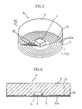
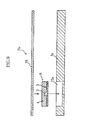
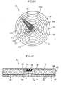
- an IC module A of this embodiment comprises a flexible substrate 1, an IC chip 2, an antenna coil 3 and a sealing resin 4.
- the IC module is cylindrical as a whole.
- the flexible substrate 1 comprises a thin flexible synthetic-resin film as a base material.
- An example of the base material is a polyimide film.
- the flexible substrate 1 is circular in plan view and has a thickness of about 0.1 mm for example.
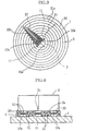
- the antenna coil 3 comprises a conductive film 30 which is patterned on an obverse surface of the flexible substrate 1.
- the conductive film 30 is a copper foil for example.
- the antenna coil 3 has a spiral portion 31 having a plurality of turns 31a, and a bent extension 32 extending radially inwardly of the spiral portion 31 from the plurality of turns 31a.
- a pair of terminals 10a, 10b are provided close to each other in the inner portion of the spiral portion 31 on the obverse surface of the flexible substrate 1 in such a manner that an inward end 32a of the bent extension 32 is placed between the terminals 10a, 10b.
- the pair of terminals 10a, 10b are lands protruding upward from the flexible substrate 1.
- the antenna coil 3 has a starting end connected to the terminal 10a.
- the bent extension 32 includes a lead 32b which provides a terminating end of the antenna coil 3.
- the lead 32b extends toward the terminal 10b from the outer periphery of the spiral portion 31 without contacting the plurality of turns 31a.
- the terminating end of the antenna coil 3 is connected to the terminal 10b while avoiding a short circuit of the antenna coil 3.
- the antenna coil 3 functions as a device for transmitting and receiving radio waves (electromagnetic waves) to and from a transmitter/receiver.
- the antenna coil 3 generates an electromagnetic force by electromagnetic induction for power supply to the IC chip 2 upon receiving radio waves.
- a memory such as an EEPROM, a capacitor, or the like is integrally built in the IC chip 2.
- the IC chip 2 is driven with the electromagnetic force inductively generated by the antenna coil 3.
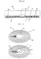
- the IC chip 2 which has the shape of a rectangular parallelepiped, has a main surface 2a formed with a pair of electrodes 20 for connection to the antenna.
- the electrodes 20 on the main surface 2a are projections located at two corners on a common diagonal line.
- a pair of dummy electrodes 21 are also formed at the other corners on the main surface 2a.
- the dummy electrodes 21 are also projections which are similar to the electrodes 20. However, the dummy electrodes 21 are not connected to the internal circuitry of the IC chip 2.
- a pair of dummy terminals 11 corresponding to the dummy electrodes 21, 21 are provided on the upper surface of the flexible substrate 1.
- the dummy terminals 11 are also projections similar to the terminals 10a, 10b, but they are held out of conduction with the antenna coil 3.
- the IC chip 2 is bonded to the obverse surface of the flexible substrate 1 via an anisotropic conductive film 5.
- the main surface 2a is directed downward with the electrodes 20 facing the terminals 10a, 10b.
- the dummy electrodes 21 faces the dummy terminals 11.
- the anisotropic conductive film 5 has conductive particles 51 such as metal particles dispersed and contained in an insulating resin 50 having adhesion.
- an epoxy resin may be used as the insulating resin 50.
- a part of the anisotropic conductive film 5 is sandwiched between each of the electrodes 20 and a respective one of the terminals 10a, 10b under a certain pressure, thereby increasing the density of the conductive particles 51 in the sandwiched part.
- the sealing resin 4 is molded to enclose the IC chip 2 and the antenna coil 3 on the obverse surface of the flexible substrate 1.
- the sealing resin 4 is a thin plate which is circular in plan view similarly to the flexible substrate 1.
- the sealing resin 4 comprises a synthetic resin whose modulus of elasticity is lower than that of a card body 7 of an IC-card B described below.
- An example includes an epoxy resin containing no strength-increasing filler.
- the sealing resin 4 covers only the obverse surface of the flexible substrate 1.
- the present invention is not limited to such a structure. A part of the sealing resin may extend to the reverse surface of the flexible substrate 1 for example.
- an antenna coil 3 may be formed by first depositing a copper foil substantially over the entire obverse surface of the flexible substrate 1 by vapor deposition, sputtering or CVD, and then etching the copper foil.
- a pair of terminals 10a, 10b and A pair of dummy terminals 11 can be also formed at the time of forming the antenna coil 3.
- an anisotropic conductive film 5 is applied onto the flexible substrate 1, and an IC chip 2 is pressed against the pair of terminals 10a, 10b.
- Such a series of process steps permits the fabrication of the antenna coil 3 while establishing electrical conduction between the antenna coil 3 and the IC chip 2, thereby considerably increasing the production efficiency.
- the electrodes 20 and the dummy electrodes 21 face the pair of terminals 10a, 10b and the pair of dummy terminals 11, respectively, whereby the IC chip 2 is supported at four points. This prevents the IC chip 2 from being inclined. Therefore, the IC chip 2 can be stably mounted on the flexible substrate 1. Further, it is possible to automate mounting of the IC chip 2 on the flexible substrate 1 with the use of an existing chip mounting apparatus.
- the antenna coil 3 Since the antenna coil 3 is provided by the patterned conductive film 30, its thickness can be rendered smaller than that of the IC chip 2. Even when the number of turns 31a of the spiral 31 is considerably increased, the antenna coil 3 will not become bulky. Accordingly, the thickness of the whole IC module A may be also reduced to about 0.45 mm for example. Further, the location of the IC chip 2 inward of the spiral 31 of the antenna coil 3 provides a good space efficiency. Therefore, the outer diameter of the whole IC module A can be also reduced.
- the distance between the paired electrodes 20 is maximum within the area of the main surface 2a.
- the distance between the paired terminals 10a, 10b can be relatively increased, thereby making it possible to increase the width of the bent extension 32 between the paired terminals 10a, 10b. Therefore, the number of turns 31a can be correspondingly increased to enhance the properties of the antenna coil 3. Since the IC chip 2 and the antenna coil 3 are protected by the sealing resin 4, the IC module A can be handled without damaging these components.
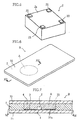
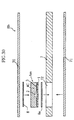
- the IC-card B is rectangular in plan view and has a thickness of about 0.76 mm for example. As clearly shown in Fig. 8, the IC-card B comprises a card body 7 and two cover sheets 70, 71 in addition to the IC module A.
- the card body 7 is made of a synthetic resin such as polyethylene terephthalate resin (hereinafter abbreviated as PET) or polyvinyl chloride (hereinafter abbreviated as PVC). Unlike the sealing resin 4, the synthetic resin for the card body 7 contains a filler as a reinforcing material. Thus, the modulus of elasticity of the card body 7 is no less than 9.8 GPa for example. By contrast, the modulus of elasticity of the sealing resin 4 is no more than 9.0 GPa for example and therefore lower than that of the card body 7.
- the card body 7 has a thickness of about 0.45 mm similarly to the IC module A.
- the card body 7 has a receiving portion 72 in the form of a through-hole for housing the IC module A.
- the two cover sheets 70, 71 are shaped to conform to the card body 7 in plan view, and have a respective thickness of about 0.15 mm for example.
- the cover sheets 70, 71 are also made of a synthetic resin such as PET or PVC similarly to the card body 7.
- the cover sheets 70, 71 are bonded to the obverse and reverse surfaces, respectively, of the card body 7 after the IC module A is housed in the receiving portion 72. Therefore, the receiving portion 72 are upwardly and downwardly closed by the respective cover sheets 70, 71, thereby enclosing the IC module A in the receiving portion 72.
- the above-described overall thickness of the IC-card includes the thickness of an adhesive layer for bonding each of the cover sheets 70, 71 to the card body 7.
- the IC module A can be appropriately housed in the receiving portion 72.
- the IC module A fitted in the receiving portion 72 has a thickness greater than the depth of the receiving portion 72, the IC module A partially projects out from the receiving portion 72.
- the IC module A may be easily compressed in its thickness direction by the cover sheets 70, 71 which are bonded to the card body 7, thereby reducing the thickness of the IC module A to be equal to the depth of the receiving portion 72.
- the IC module A can be appropriately encapsulated in the receiving portion 72.
- the cover sheets 70, 71 bonded tightly to both surfaces of the IC module A prevents the IC module A from being inappropriately displaced in the receiving portion 72.
- the manufacture of the IC module A and the card body 7 is facilitated because the thickness of the IC module A does not need to exactly coincide with the depth of the receiving portion 72.
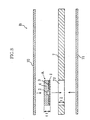
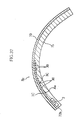
- the IC-card B is thin and flat to provide flexibility.
- a bending stress M may be exerted near the IC module A when the IC-card B is wholly or partially bent, as shown in Fig. 7.
- the sealing resin 4 of the IC module A is deformed in the same manner as the card body 7 following the bending deformation of the card body 7 because the modulus of elasticity of the sealing resin 4 is lower than that of the card body 7.
- a bending deformation of the sealing resin 4 generates a strain at the boundary between the sealing resin 4 and the IC chip 2.
- the low modulus of elasticity of the sealing resin 4 is low, it is possible to reduce the stress resulting from the strain of the sealing resin 4 .
- the IC chip 2 is prevented from significantly damaged even if a bending force is applied to the IC-card B. As a result, it is possible to prevent a loss of the data stored in the IC chip 2 which might occur due to a damage of the IC chip 2.
- An IC-card Ba shown in Fig. 9 includes a receiving portion 72a in the form of a bottomed recess formed in a card body 7a.
- the receiving portion 72a houses an IC module A. According to this structure, only a single cover sheet 70 need be bonded to the card body 7a, thereby reducing the number of the components required for the IC-card.
- An IC module Aa shown in Figs. 10 and 11 includes an antenna coil 3A which structurally differs from the antenna coil 3.
- the antenna coil 3A has a spiral portion 31 formed on the obverse surface of the flexible substrate 1, as is also the case with the antenna coil 3.
- the antenna coil 3A includes a lead 33 formed on the obverse surface of the flexible substrate 1 in connection to a terminal 10b, and a lead 34 formed on the reverse surface of the flexible substrate 1.
- the flexible substrate 1 is provided with a pair of through-holes 12a and 12b at positions inwardly and outwardly, respectively, of the spiral portion 31.
- a terminating end 31b of the spiral portion 31 conducts to one end of the lead 34 via the through-hole 12a.
- the other end of the lead 34 is connected to the lead 33 via the through-hole 12b.
- the starting and terminating ends of the antenna coil 3A can be also located at an inner position of the spiral portion 31 without short-circuiting of the antenna coil 3A, thereby providing the same advantages as the IC module A.
- the antenna coil may be formed by utilizing both of the obverse and reverse surfaces of the flexible substrate 1.
- An IC module Ab shown in Fig. 12 includes a film 19 separate from a flexible substrate 1 which carries an IC chip 2 at the center thereof.
- the film 19 may be made of polyimide for example.
- the film is centrally formed with a hole 19a which is larger in size than the IC chip 2.
- a conductor pattern 39 is formed on one surface of the film 19.
- the conductor pattern 39 is symmetrical or substantially symmetrical to the antenna coil 3 on the obverse surface of the flexible substrate 1.
- the film 19 is laid on and bonded to the obverse surface of the flexible substrate 1, so that the pattern of the antenna coil 3 and the conductor pattern 39 face each other.
- the IC chip 2 protrudes upward through the hole 19a.
- the flexible substrate 1 and the film material 19 are bonded to each other via an anisotropic conductive film 5A which is similar in property to the anisotropic conductive film 5.
- the pattern of the antenna coil 3 and the conductor pattern 39 conduct to each other through the conductive particles 51 of the anisotropic conductive film 5A.
- the thickness of the antenna coil 3 is virtually increased by as much as the sum of the size of the conductive particles 51 and the thickness of the conductor pattern 39.
- the inherent characteristics of the antenna coil 3 can be greatly improved as in the case of an antenna coil made of a relatively thick metal wire.
- There is a limitation on increasing the thickness of a conductor film 30 for the antenna coil 3 if it is formed on the obverse surface of the flexible substrate 1 only by sputtering, vapor deposition or CVD.
- the pattern is more sophisticated, it becomes more difficult to increase the thickness of the conductive film 30, resulting in an increasing loss of the intended antenna function. Such a problem is appropriately eliminated in the IC module Ab.
- the IC module Ab may also have a structure in which the IC chip 2 is enclosed in a sealing resin 4.
- the IC chip 2 is exposed above the film 19 through the hole 19a, whereby the IC chip 2 can be appropriately sealed by the sealing resin 4 when the upper surface of the film 19 is covered with the sealing resin 4.
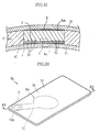
- Figs. 15 and 16 illustrates an IC module Ac which comprises a sealing resin 4A for enclosing an IC chip 2 and an antenna coil 3, and the sealing resin 4A has a plurality of perforations 40 as weakening portions.
- Each of the plural perforations 40 penetrates through the sealing resin 4A in the thickness direction of the sealing resin 4A.
- the perforations 40 are arcuate in plan view to surround the IC chip 2.
- the perforations 40 maybe formed at the time of molding the sealing resin 4A.
- the stress is concentrated at the perforations 40 to prevent the IC chip 2 from being intensively stressed. More specifically, when the IC module Ac is flexed, the width of each perforation 40 is increased or reduced. Such a deformation buffers the stress generated in the sealing resin 4A, thereby reducing the stress applied to the IC chip 2. It is therefore possible to prevent the IC chip 2 from being significantly damaged even if the IC-card incorporating the IC module Ac is flexed in use.
- the weakening portions formed in the sealing resin 4A may be variously modified in design.
- An IC module Ad shown in Fig. 17 includes a sealing resin 4A having a plurality of cylindrical perforations 41 which penetrate through the sealing resin 4A in the thickness direction thereof.
- the perforations 41 are arranged in such an arrangement as to surround the IC chip 2 in plan view.
- such a design also reduces the stress applied to the sealing resin 4A by the deformation of the perforations 41, thereby preventing the IC chip 2 from being subjected to a large stress.
- the weakening portions in the sealing resin may be provided by pin holes which are diametrically smaller than the perforations 41.
- An IC module Ae shown in Fig. 18 includes a sealing resin 4A having an obverse surface formed with a plurality of bottomed recesses 42 of a suitable depth as weakening portions.
- the recesses may be variously shaped. According to the present invention, in this way, suitably shaped recesses formed in the obverse surface of the sealing resin may provide weakening portions, and the number of such weakening portions may be optionally selected.
- a substrate for carrying an IC chip may be provided with weakening portions.
- an IC module Af shown in Fig. 19 has a flexible substrate 1 which is formed with a plurality of perforations 24 around the IC chip 2 as weakening portions.
- the perforations 24 may be formed by etching the flexible substrate 1 after forming the pattern of the antenna coil 3 on the obverse surface of the flexible substrate 1.
- the perforations 24 may be formed in the flexible substrate 1 in advance by pressing, and then the pattern of the antenna coil 3 may be formed on the obverse surface of the flexible substrate 1 to circumvent the perforations 24.
- the weakening portions may be formed either in the sealing resin or the substrate for preventing intensive application of a stress to the IC chip.
- the weakening portions may be formed in both of the sealing resin 4A and the flexible substrate 1.
- An IC module Ag shown in Fig. 20 comprises a flexible substrate 1 which is provided with a plurality of radial slits 25 extending inward from the peripheral edge of the flexible substrate 1.
- the IC chip 2 is mounted at the center of the flexible substrate 1 inwardly from the slits 25.
- the slits 25 may be formed by etching the flexible substrate 1 after forming the pattern of an antenna coil 3 on the flexible substrate 1.
- the IC module Ag also includes a sealing resin package made of e.g. a thermosetting epoxy resin for enclosing the IC chip 2 and the antenna coil 3.
- the sealing process may be performed by supplying a sealing resin fluidized at high temperature into a mold, and then allowing the sealing resin to harden under heating. With a temperature drop after the molding process, the sealing resin shrinks while it remains bonded to the flexible substrate 1.
- the flexible substrate 1 made of e.g. polyimide differs in linear expansion coefficient from the sealing resin.
- the shrinkage of the sealing resin causes the flexible substrate 1 to be considerably warped due to a difference in shrinkage between the flexible substrate and the sealing resin, so that a stress resulting from the warping may be applied to the IC chip 2.
- the flexible substrate 1 of the IC module Ag can deform to reduce the width of the slits 25 when the sealing resin shrinks, so that the width reduction of the slits 25 takes the place of the shrinkage of the flexible substrate 1 as a whole. Therefore, at least the center of the flexible substrate 1 is prevented from warping to a large extent, thereby protecting the IC chip 2.
- An IC module Ah shown in Fig. 21 comprises a flexible substrate 1A having radially extending projections 26 centered about a portion on which an IC chip 2 is mounted.
- the flexible substrate 1A as a whole is shaped like a gear or a starfish in plan view.
- the spacing between the projections 26 reduces with a shrinkage of a sealing resin occurring due to a temperature drop after molding the sealing resin in intimate bonding contact with the obverse surface of the flexible substrate 1A to enclose the IC chip 2 and an antenna coil 3B. Therefore, the flexible substrate 1A is prevented from being greatly warped, thereby protecting the IC chip 2, as in the case of the IC module Ag.
- the pattern of an antenna coil 3B is also shaped like a gear or a starfish in plan view in conformity with the shape of the flexible substrate 1A. Due to such a configuration, since the pattern of the antenna coil 3B extends radially on the projections 26 of the flexible substrate 1A, the pattern of the antenna coil 3B on the projections 26 does not hinder shrinkage of the sealing resin 4. Thus, the flexible substrate 1A is prevented from inappropriately deforming due to a shrinkage hindrance provided by the antenna coil 3B.
- the sealing resin for sealing the IC chip 2 and the antenna coil 3B is also shaped like a gear or a starfish in plan view to have a plurality of projections in conformity with the shape of the flexible substrate 1A.
- the sealing resin shrinks with a reduction of the spacing between the projections of the sealing resin.
- the warping of the flexible substrate 1A in its thickness direction is correspondingly reduced, so that the IC chip 2 is protected against damage even more reliably.
- the projections 26 of the flexible substrate 1A and the corresponding projections of the sealing resin are locally flexed to allow for the bending of the IC-card. Therefore, it is possible to avoid stress concentration on the IC chip 2 for protection thereof.
- An IC module Ai shown in Fig. 22 has a flexible substrate 1B whose material is PET. As shown in Figs. 23 and 24, a bond assisting layer 35 is formed at a portion of the flexible substrate 1B on which an adhesive layer 5B is applied for bonding the IC chip 2 to the flexible substrate 1B.
- the bond assisting layer 35 comprises an inner end 32a of the bent extension 32 of the antenna coil 3 and a dummy pattern 35a formed near the inner end 32a.
- the dummy pattern 35a may be provided by the conductive film 30 which is patterned on the obverse surface of the flexible substrate 1B to have a plurality of stripe lines at the time of patterning the antenna coil 3.
- the dummy pattern 35a may be made of the same material, such as copper, as the antenna coil 3.
- the adhesive layer 5B may be made of an anisotropic conductive film for example, like the anisotropic conductive film 5.
- the use of the PET flexible substrate 1B is advantageous for its lower cost in comparison with a polyimide flexible substrate.
- the use of the PET flexible substrate 1B normally results in lower adhesion between the flexible substrate 1B and the adhesive layer 5B. Since the adhesive layer 5B firmly adheres to an object by means of molecular hydrogen bonding, it cannot provide a sufficient adhesion if the object is made of PET having no molecular part which induces such hydrogen bonding. In the IC module Ai, however, the adhesive layer 5B also adheres to the surfaces of the bond assisting layer 35. Since the bond assisting layer 35 is made of copper, the adhesive layer 5B firmly adheres to the bond assisting layer 35.
- the dummy pattern 35a increases the surface area of the bond assisting layer 35, it further enhances the adhesion between the flexible substrate 1B and the bond assisting layer 35. As a result, the IC chip 2 can be reliably held on the flexible substrate 1B. Further, since the dummy pattern 35a may be formed together with the pattern of the antenna coil 3, it does not complicates the manufacturing process of the IC module Ai.
- Fig. 25 shows an IC module Aj wherein a bond assisting layer 35A is provided by a bent extension 32 of an antenna coil 3 and a dummy pattern 35b each including a plurality of curved lines.
- Fig. 26 shows an IC module Ak wherein a dummy pattern 35 serving as a bond assisting layer 35B includes a plurality of dotted lines. In this way, the bond assisting layer may be variously modified in configuration.
- Each of the IC modules Ai to Ak is reasonable in that a part (inner end 32a) of the antenna coil 3 is utilized for improvement of the adhesion of the adhesive layer 5B.
- the dummy pattern may be obviated, and a part of the antenna coil 3 alone may serve as a bond assisting layer. Therefore, though no means is provided which corresponds to the dummy pattern in the embodiment illustrated in Fig. 3, the inner end 32a of the antenna coil 3 shown in that figure considered as the bond assisting layer according to the present invention.
- the antenna coil 3 need not be utilized, and the bond assisting layer may, of course, be made only of an entirely different material than the antenna coil 3.
- An IC module Al shown in Figs. 27 and 28 comprises a covering member 4B for covering the IC chip 2 and an elastic member 49.
- the covering member 4B includes a first sheet 43 having a through-hole 45a, and a second sheet 44 bonded to one surface of the first sheet 43. Since an end opening of the through-hole 45a is closed by the second sheet 44, the through-hole 45a provides a recess 45 having one open end.
- the first and second sheets 43, 44 are made of ABS resin for example.
- the thickness of the first sheet 43 is about 0.25 mm for example which is larger than the thickness of the IC chip 2.
- the thickness of the second sheet 44 is about 0.1 mm for example.
- the covering member 4B is bonded to the obverse surface of the flexible substrate 1 with the opening of the recess 45 directed downward.
- the IC chip 2 is housed in the recess 45 and covered by the covering member 4B.
- the elastic member 49 is made of a silicone rubber for example to be elastomeric. The elastic member 49 is appropriately compressed between the upper surface of the IC chip 2 and the inner top wall of the recess 45.
- the IC chip 2 is always pressed against the obverse surface of the flexible substrate 1 by the elastic restoring force of the elastic member 49.
- the electrodes 20 of the IC chip 2 can be always pressed toward the terminals 10a, 10b even if the IC module A is somewhat deformed under bending, thereby reliably establishing conduction between the IC chip 2 and the antenna coil 3.
- the IC module Al does not utilizes an adhesive for mounting the IC chip 2 on the flexible substrate 1, so that an adhesive applying step may be eliminated in the manufacturing process.
- the covering member 4B serves to protect the IC chip 2.
- the covering member 4B including the two bonded sheets can be manufactured easily.
- the present invention is not limited to such a structure.
- the covering member may be resin-molded to have a recess, and thereafter bonded to the flexible substrate 1.
- An IC-card Bb shown in Figs. 29 and 30 comprises flexible sheets 8, 8a each of which is provided between an IC module Am and a respective one of cover sheets 70, 71 bonded to both surfaces of a card body 7.
- the flexible sheets 8, 8a are housed in a receiving portion 72 together with the IC module Am.
- the flexible sheets 8, 8a are shaped and sized similarly to the IC module Am in plan view, and have an appropriate thickness.
- the flexible sheets 8, 8a have a lower modulus of elasticity than a sealing resin 4C.
- the flexible sheets may be made of a thermosetting epoxy resin containing no filler. Both surfaces of the flexible sheet 8 are bonded to the sealing resin 4C of the IC module Am and the cover sheet 70, respectively.
- both surfaces of the flexible sheet 8a are bonded to the flexible substrate 1 of the IC module A and the cover sheet 71, respectively.
- each of the flexible sheets 8, 8a is sandwiched between the IC module Am and a respective one of the cover sheets 70, 71 and thereafter pressed under heating for fusion.
- the flexible sheets 8, 8a In the IC-card Bb, when the card body 7 and the two cover sheets 70, 71 are deformed under bending, the flexible sheets 8, 8a also deformed correspondingly, as shown in Fig. 31. Since the flexible sheets 8, 8a have a lower modulus of elasticity than the sealing resin 4C, they start deforming prior to deformation of the sealing resin 4C. More specifically, each of the flexible sheets 8, 8a are deformed between the IC module Am and a respective one of the cover sheets 70, 71 to increase or reduce in thickness according to the bending deformation of the cover sheets 70, 71. Such deformation of the flexible sheets 8, 8a prevents the bending force of the cover sheets 70, 71 from being directly applied to the IC module Am. As a result, it is possible to prevent the IC module Am from being greatly flexed with the same curvature of the cover sheets 70, 71, thereby protecting the IC chip 2 while preventing disconnection of the antenna coil 3.
- the flexible member When a flexible member is interposed between the IC module and each cover sheet for protecting the IC module as in the IC-card Bb, the flexible member does not have to be necessarily housed in the receiving portion of the cover member.
- the flexible member may be provided over the surface between the card body and the cover sheet.
- the flexible member may also function to firmly bond the card body to the cover sheet, thereby effectively preventing the cover sheet from coming off the card body.
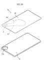
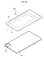
- An IC-card Bc shown in Fig. 32 comprises an IC module An sandwiched between a card body 7b and a cover sheet 70 bonded to the card body in overlapping relationship.
- the card body 7b is rectangular in plan view and has a bottomed recess 72b at one of the four corners of the card body 7b.
- the IC module An comprises an antenna coil 3C which is formed by patterning a conductive film 30 on the obverse surface of a flexible substrate 1C on which the IC chip 2 is mounted.
- the antenna coil 3C has a bent portion 32C extending outwardly of a spiral portion 31C from a plurality of spiral turns 31a.
- a pair of terminals 10c, 10d connected to the starting and terminating ends of the antenna coil 3C are disposed outside the spiral portion 31C. Accordingly, the IC chip 2 mounted in conduction with the pair of terminals 10c, 10d is also disposed outside the spiral portion 31C.
- the IC module An is bonded to one surface of the cover sheet 70, and the IC chip 2 is held by the cover sheet 70.
- the IC chip 2 of the IC module An is housed in the recess 72b, and the antenna coil 3C may be located near the center of the card body 7b and the cover sheet 70 rather than the IC chip 2.
- a gap is provided between the outer surfaces of the IC chip 2 and the inner wall surfaces of the recess 72b for preventing the IC chip 2 from directly contacting the card body 7b.
- the IC chip 2 is held attached to the cover sheet 70 in the recess 72b without contacting the card body 7b. Therefore, it is possible to prevent the card body 7b from strongly contacting the IC chip 2, thereby reliably protecting the IC chip 2.
- the spiral portion 31C of the antenna coil 3C generates an electromotive force by electromagnetic induction.
- the IC chip 2 is located away from the spiral portion 31C, the IC chip 2 is little influenced by noises which may be caused by the electromagnetic induction, consequently reducing the likelihood of malfunction.
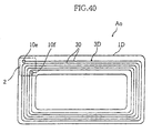
- Figs. 38 and 39 show an IC-card Bd wherein an IC module Ao disposed between a card body 7b and a cover sheet 70 differs from the above-described IC module An in design.
- the IC module Ao includes an antenna coil 3D formed on the obverse surface of the flexible substrate 1B, and the antenna coil has a spiral portion 31D which includes a plurality of spiral turns 31d extending along a rectangular path in plan view.
- the flexible substrate 1B is rectangular and has an opening inwardly of the spiral portion 31D.
- Each of paired terminals 10e, 10f connected to the starting and terminating ends of the antenna coil 3D is disposed outside or inside, respectively, of the spiral portion 31D at a corner of the flexible substrate 1B.
- the IC chip 2 is provided at the above-described corner of the flexible substrate 1B in conduction with the pair of terminals 10e, 10f.
- the IC module Ao is bonded to the cover sheet 70.
- the IC chip 2 is substantially retained by the cover sheet 70 and housed in the recess 72b at a corner of the card body 7b.
- a gap is formed between the inner wall surfaces of the recess 72b and the outer surfaces of the IC chip 2.
- the IC-card Bd can prevent a damage to the IC chip 2 even if the card body 7b and the cover sheet 70 are deformed under bending.
- the antenna coil 3D of the IC-card Bd has a simple pattern for facilitating its manufacture. It is also easy to increase the number of turns and the winding density of the antenna coil 3D.
- the particular pattern of the antenna coil may be variously modified.
- the particular shape of the recess 72b of the IC module An or Ao is not limitative.
- the IC chip may be provided at a peripheral portion of the card member other than a corner thereof, instead of arranging the IC chip at or near a corner of the card member. This is because a peripheral portion of the card member deforms less than at a central portion of the card member, and therefore prevents a large damage to the IC chip.
- IC module and the IC chip illustrated in the above embodiments are not limitative but may be modified variously according to the present invention.
- a hard substrate with little flexibility may be used for mounting the IC chip.
- An IC module according to the present invention may be used as a component of an IC-card.
- An IC-card according to the present invention may be used as a portable storage medium for storing various data.
Abstract
Description
- The present invention relates to an IC module which is a component of an IC-card used as an ID card or the like. It also relates to an IC-card including such an IC module.
- An IC-card having an IC memory is known as a card having an information storage function. Recently, a non-contact IC-card has been in practical use as a prepaid card for use of ski lifts or the like. Such an IC-card includes an IC chip incorporated in a card member made of a synthetic resin. More particularly, the IC-card comprises an IC module which is incorporated in a card member made of a synthetic resin and having a predetermined thickness, and the IC-card module comprises an electronic circuit including an IC memory and an antenna coil.
- The antenna coil not only provides its inherent function as an antenna for transmitting and receiving radio waves but also has a function of supplying a drive power to the IC chip by inductively generating an electromotive force upon receiving radio waves. Therefore, an IC-card incorporating an antenna coil can eliminate the need for incorporating a power source. Such an IC-card requires a further thickness reduction.
- A conventional antenna coil utilizes a wire-wound coil formed of a metal wire. The wire-wound coil has a structure in which the metal wire is wound about 50 turns, for example, so that it has a large thickness. If the number of wire turns is reduced in order to reduce the thickness of the wire-wound coil, the properties of the antenna may be degraded. Consequently, the wire-wound coil becomes inevitably bulky, and there is a limitation on the thickness reduction of an IC-card. Further, in manufacturing the IC-card, the wire-wound coil and the IC chip, prepared separately, need to be aligned with each other, and the ends of the wire-wound coil must be connected to the electrodes of the IC chip in such a manner that they do not positionally deviate relative to each other. Accordingly, the series of the manufacturing steps is very complicated to result in a poor production efficiency. Furthermore, the wire-wound coil is liable to disconnection when the IC-card is deformed under bending for example.
- An IC modul according to the preamble of
claim 1 is known from EP-A-0 737 935. - An object of the present invention is to provide an IC module and an IC-card capable of solving or reducing the above problems.
- A first aspect of the present invention provides an IC module according to
claim 1. - Preferably, the bent extension has an inner end interposed between the starting and terminating ends of the antenna coil.
- Preferably, the main surface of the IC chip is rectangular in plan view. The pair of electrodes for antenna connection are disposed at corners of the main surface on a common diagonal line.
- Preferably, the main surface of the IC chip is provided with at least one dummy electrode. The substrate is provided with a dummy terminal corresponding to the dummy electrode, and the dummy electrode is connected to the dummy terminal.
- Preferably, the substrate comprises a flexible substrate made of a resin film as a base material.
- Preferably, the IC module further comprises a film having a surface formed with a conductor pattern which is symmetrical or substantially symmetrical to the pattern of the antenna coil. The substrate and the film material are bonded to each other to bring the conductive film pattern of the antenna coil into connection to the conductor pattern of the film.
- Preferably, the film has a hole for avoiding interference of the film with the IC chip.
- Preferably, the substrate and the film are bonded to each other via an anisotropic conductive film comprising conductive particles dispersed in an insulating resin.
- Preferably, the IC module further comprises an adhesive layer for bonding the substrate and the IC chip to each other, and a bond assisting layer disposed at a portion of the substrate for adhesion to the adhesive layer. The bond assisting layer is made of a material having a higher adhesion to the adhesive layer than the substrate.
- Preferably, the bond assisting layer is provided by the conductive film which also provides the antenna coil.
- Preferably, a part of the antenna coil provides the bond assisting layer.
- Preferably, the adhesive layer comprises an anisotropic conductive film including conductive particles dispersed in an insulating resin.
- Preferably, the substrate has weakening means adjacent the IC chip.
- Preferably, the weakening means comprises a plurality of perforations penetrating through the substrate around the IC chip.
- Preferably, the IC module further comprises a sealing member for enclosing the IC chip.
- Preferably, the sealing member has weakening means.
- Preferably, the weakening means comprises a perforation which penetrates through the sealing member in its thickness direction.
- Preferably, the weakening means comprises a recess formed on an obverse surface of the sealing member.
- Preferably, the weakening means comprises a plurality of weakening portions arranged to surround the IC chip in plan view.
- Preferably, the IC chip is mounted at a central portion of the substrate. The substrate is formed with a plurality of slits extending from a peripheral edge of the substrate toward the central portion.
- Preferably, the IC chip is mounted at a central portion of the substrate. The substrate is shaped like a gear or a starfish in plan view with a plurality of projections extending radially from a portion of the substrate on which the IC chip is mounted.
- Preferably, the antenna coil is shaped like a gear or a starfish in plan view in conformity with the shape of the substrate.
- Preferably, the sealing member is shaped like a gear or a starfish in plan view in conformity with the shape of the substrate.
- Preferably, the IC module further comprises a covering member which is bonded to the substrate for covering the IC chip, and an elastic member interposed between the covering member and the IC chip. The IC chip is pressed against the substrate by the elastic member.
- Preferably, the covering member has a recess for housing the IC chip.
- Preferably, the covering member comprises a first sheet having a through-hole, and a second sheet bonded to the first sheet to close an opening of the through-hole at one end thereof.
- According to a second aspect of the present invention, there is provided an IC-card according to claim 27.
- Preferably, the card member comprises a card body having a receiving portion for housing the IC module, and at least one cover sheet bonded to the card body to close an opening of the receiving portion.
- Preferably, the IC module includes a sealing member for sealing the IC chip. The sealing member has a lower modulus of elasticity than the card body.
- Preferably, the substrate comprises a flexible substrate made of a flexible resin film as a base material.
- Preferably, the IC module includes a sealing member for sealing the IC chip. The IC module and the cover sheet are bonded to each other via a flexible member which is lower in modulus of elasticity than the sealing member.
- Preferably, the flexible member comprises a sheet made of a thermosetting resin.
- Various features and advantages of the present invention will become clearer from the following description of embodiments given with reference to the accompanying drawings.
-
- Fig. 1 is a perspective view showing an example of IC module according to the present invention.
- Fig. 2 is a sectional view taken along lines X1-X1 in Fig. 1.
- Fig. 3 is a plan view of a substrate and an antenna coil of the IC module shown in Fig. 1.
- Fig. 4 is an enlarged fragmentary sectional view showing a principal portion of the IC module shown in Fig. 1.
- Fig. 5 is a perspective view showing an example of IC chip.
- Fig. 6 is a perspective view showing an example of IC-card according to the present invention.
- Fig. 7 is a sectional view taken along lines X2-X2 in Fig. 6.
- Fig. 8 is an exploded sectional view of the IC-card shown in Fig. 6.
- Fig. 9 is an exploded sectional view showing another example of IC-card according to the present invention.
- Fig. 10 is a perspective view showing a substrate and an antenna coil in an illustrative example of an IC module.
- Fig. 11 is a sectional view taken along lines X3-X3 in Fig. 10.
- Fig. 12 is a sectional view showing another example of IC module according to the present invention.
- Fig. 13 is an exploded perspective view showing principal components of the IC module shown in Fig. 12.
- Fig. 14 is an enlarged view showing the portion encircled at N1 in Fig. 12.
- Fig. 15 is a perspective view showing a further example of IC module according to the present invention.
- Fig. 16 is a sectional view taken along lines X4-X4 in Fig. 15.
- Fig. 17 is a perspective view showing a further example of IC module according to the present invention.
- Fig. 18 is a perspective view showing a further example of IC module according to the present invention.
- Fig. 19 is a perspective view showing a further example of IC module according to the present invention.
- Fig. 20 is a plan view showing a further example of IC module according to the present invention.
- Fig. 21 is a plan view showing a further example of IC module according to the present invention.
- Fig. 22 is a sectional view showing a further example of IC module according to the present invention.
- Fig. 23 is a plan view showing a substrate and an antenna coil of the IC module shown in Fig. 22.
- Fig. 24 is a partially enlarged sectional view of the IC module shown in Fig. 22.
- Fig. 25 is a plan view showing a further example of IC module according to the present invention.
- Fig. 26 is a plan view showing a further example of IC module according to the present invention.
- Fig. 27 is a sectional view showing a further example of IC module according to the present invention.
- Fig. 28 is a partially enlarged sectional view of the IC module shown in Fig. 27.
- Fig. 29 is a fragmentary sectional view showing a further example of IC-card according to the present invention.
- Fig. 30 is an exploded sectional view of the IC-card shown in Fig. 29.
- Fig. 31 is a fragmentary sectional view showing the IC-card of Fig. 29 in a bent state.
- Fig. 32 is a perspective view showing an illustrative example of an IC-card.
- Fig. 33 is an exploded perspective view of the IC-card shown in Fig. 32.
- Fig. 34 is a sectional view taken on line X5-X5 of Fig. 32.
- Fig. 35 is an exploded sectional view of the IC-card shown in Fig. 32.
- Fig. 36 is a view illustrating an IC module of the IC-card shown in Fig. 32.
- Fig. 37 is a sectional view showing the IC-card of Fig. 32 in a bent state.
- Fig. 38 is an exploded perspective view showing an illustrative example of an IC-card.
- Fig. 39 is an exploded sectional view of the IC-card shown in Fig. 38.
- Fig. 40 is a view illustrating an IC module of the IC-card shown in Fig. 38.
-
- Embodiments of the present invention will be described below with reference to the accompanying drawings.
- In Figs. 1 and 2, an IC module A of this embodiment comprises a
flexible substrate 1, anIC chip 2, anantenna coil 3 and a sealingresin 4. The IC module is cylindrical as a whole. - The
flexible substrate 1 comprises a thin flexible synthetic-resin film as a base material. An example of the base material is a polyimide film. Theflexible substrate 1 is circular in plan view and has a thickness of about 0.1 mm for example. - The
antenna coil 3 comprises aconductive film 30 which is patterned on an obverse surface of theflexible substrate 1. Theconductive film 30 is a copper foil for example. As shown in Fig. 3, theantenna coil 3 has aspiral portion 31 having a plurality ofturns 31a, and abent extension 32 extending radially inwardly of thespiral portion 31 from the plurality ofturns 31a. A pair ofterminals spiral portion 31 on the obverse surface of theflexible substrate 1 in such a manner that aninward end 32a of thebent extension 32 is placed between theterminals terminals flexible substrate 1. Theantenna coil 3 has a starting end connected to the terminal 10a. On the other hand, thebent extension 32 includes a lead 32b which provides a terminating end of theantenna coil 3. The lead 32b extends toward the terminal 10b from the outer periphery of thespiral portion 31 without contacting the plurality ofturns 31a. Thus, the terminating end of theantenna coil 3 is connected to the terminal 10b while avoiding a short circuit of theantenna coil 3. Theantenna coil 3 functions as a device for transmitting and receiving radio waves (electromagnetic waves) to and from a transmitter/receiver. In addition, theantenna coil 3 generates an electromagnetic force by electromagnetic induction for power supply to theIC chip 2 upon receiving radio waves. - A memory such as an EEPROM, a capacitor, or the like is integrally built in the
IC chip 2. TheIC chip 2 is driven with the electromagnetic force inductively generated by theantenna coil 3. As better shown in Fig. 5, theIC chip 2, which has the shape of a rectangular parallelepiped, has amain surface 2a formed with a pair ofelectrodes 20 for connection to the antenna. Theelectrodes 20 on themain surface 2a are projections located at two corners on a common diagonal line. A pair ofdummy electrodes 21 are also formed at the other corners on themain surface 2a. Thedummy electrodes 21 are also projections which are similar to theelectrodes 20. However, thedummy electrodes 21 are not connected to the internal circuitry of theIC chip 2. As better shown in Fig. 3, a pair ofdummy terminals 11 corresponding to thedummy electrodes flexible substrate 1. Thedummy terminals 11 are also projections similar to theterminals antenna coil 3. - As clearly shown in Fig. 4, the
IC chip 2 is bonded to the obverse surface of theflexible substrate 1 via an anisotropicconductive film 5. Themain surface 2a is directed downward with theelectrodes 20 facing theterminals dummy electrodes 21 faces thedummy terminals 11. The anisotropicconductive film 5 hasconductive particles 51 such as metal particles dispersed and contained in an insulatingresin 50 having adhesion. For instance, an epoxy resin may be used as the insulatingresin 50. A part of the anisotropicconductive film 5 is sandwiched between each of theelectrodes 20 and a respective one of theterminals conductive particles 51 in the sandwiched part. As a result, an electrical conduction is provided only between each of theelectrodes 20 and a respective one of theterminals conductive particles 51 is also increased at a portion between each of thedummy electrodes 21 and a respective one of thedummy terminals 11, but this portion has nothing to do with electrical connection between theIC chip 2 and theantenna coil 3. - As shown in Figs. 1 and 2, the sealing
resin 4 is molded to enclose theIC chip 2 and theantenna coil 3 on the obverse surface of theflexible substrate 1. The sealingresin 4 is a thin plate which is circular in plan view similarly to theflexible substrate 1. The sealingresin 4 comprises a synthetic resin whose modulus of elasticity is lower than that of acard body 7 of an IC-card B described below. An example includes an epoxy resin containing no strength-increasing filler. The sealingresin 4 covers only the obverse surface of theflexible substrate 1. However, the present invention is not limited to such a structure. A part of the sealing resin may extend to the reverse surface of theflexible substrate 1 for example. - In manufacturing an IC module A, an
antenna coil 3 may be formed by first depositing a copper foil substantially over the entire obverse surface of theflexible substrate 1 by vapor deposition, sputtering or CVD, and then etching the copper foil. A pair ofterminals dummy terminals 11 can be also formed at the time of forming theantenna coil 3. After the formation of theantenna coil 3, an anisotropicconductive film 5 is applied onto theflexible substrate 1, and anIC chip 2 is pressed against the pair ofterminals antenna coil 3 while establishing electrical conduction between theantenna coil 3 and theIC chip 2, thereby considerably increasing the production efficiency. - The
electrodes 20 and thedummy electrodes 21 face the pair ofterminals dummy terminals 11, respectively, whereby theIC chip 2 is supported at four points. This prevents theIC chip 2 from being inclined. Therefore, theIC chip 2 can be stably mounted on theflexible substrate 1. Further, it is possible to automate mounting of theIC chip 2 on theflexible substrate 1 with the use of an existing chip mounting apparatus. - Since the
antenna coil 3 is provided by the patternedconductive film 30, its thickness can be rendered smaller than that of theIC chip 2. Even when the number ofturns 31a of the spiral 31 is considerably increased, theantenna coil 3 will not become bulky. Accordingly, the thickness of the whole IC module A may be also reduced to about 0.45 mm for example. Further, the location of theIC chip 2 inward of thespiral 31 of theantenna coil 3 provides a good space efficiency. Therefore, the outer diameter of the whole IC module A can be also reduced. - Since the paired
electrodes 20 are located at the corners on a common diagonal line on themain surface 2a of theIC chip 2, the distance between the pairedelectrodes 20 is maximum within the area of themain surface 2a. Thus, the distance between the pairedterminals bent extension 32 between the pairedterminals turns 31a can be correspondingly increased to enhance the properties of theantenna coil 3. Since theIC chip 2 and theantenna coil 3 are protected by the sealingresin 4, the IC module A can be handled without damaging these components. - Next, reference is made to Figs. 6 through 8a for explaining an IC-card B which incorporates the above-described IC module A.
- Referring to Fig. 6, the IC-card B is rectangular in plan view and has a thickness of about 0.76 mm for example. As clearly shown in Fig. 8, the IC-card B comprises a
card body 7 and twocover sheets - The
card body 7 is made of a synthetic resin such as polyethylene terephthalate resin (hereinafter abbreviated as PET) or polyvinyl chloride (hereinafter abbreviated as PVC). Unlike the sealingresin 4, the synthetic resin for thecard body 7 contains a filler as a reinforcing material. Thus, the modulus of elasticity of thecard body 7 is no less than 9.8 GPa for example. By contrast, the modulus of elasticity of the sealingresin 4 is no more than 9.0 GPa for example and therefore lower than that of thecard body 7. Thecard body 7 has a thickness of about 0.45 mm similarly to the IC module A. Thecard body 7 has a receivingportion 72 in the form of a through-hole for housing the IC module A. - The two
cover sheets card body 7 in plan view, and have a respective thickness of about 0.15 mm for example. Thecover sheets card body 7. Thecover sheets card body 7 after the IC module A is housed in the receivingportion 72. Therefore, the receivingportion 72 are upwardly and downwardly closed by therespective cover sheets portion 72. The above-described overall thickness of the IC-card includes the thickness of an adhesive layer for bonding each of thecover sheets card body 7. - As clearly shown in Fig. 8, even if the thickness t1 of the IC module A in the IC-card B is slightly greater than the depth of the receiving portion 72 (i.e., the thickness t2 of the card body 7), the IC module A can be appropriately housed in the receiving
portion 72. When the IC module A fitted in the receivingportion 72 has a thickness greater than the depth of the receivingportion 72, the IC module A partially projects out from the receivingportion 72. However, due to the low modulus of elasticity of the sealingresin 4, the IC module A may be easily compressed in its thickness direction by thecover sheets card body 7, thereby reducing the thickness of the IC module A to be equal to the depth of the receivingportion 72. As a result, the IC module A can be appropriately encapsulated in the receivingportion 72. In this manner, thecover sheets portion 72. The manufacture of the IC module A and thecard body 7 is facilitated because the thickness of the IC module A does not need to exactly coincide with the depth of the receivingportion 72. - The IC-card B is thin and flat to provide flexibility. Thus, a bending stress M may be exerted near the IC module A when the IC-card B is wholly or partially bent, as shown in Fig. 7. In this case, the sealing
resin 4 of the IC module A is deformed in the same manner as thecard body 7 following the bending deformation of thecard body 7 because the modulus of elasticity of the sealingresin 4 is lower than that of thecard body 7. Though such a bending deformation of the sealingresin 4 generates a strain at the boundary between the sealingresin 4 and theIC chip 2. However, since the low modulus of elasticity of the sealingresin 4 is low, it is possible to reduce the stress resulting from the strain of the sealingresin 4 . Therefore, theIC chip 2 is prevented from significantly damaged even if a bending force is applied to the IC-card B. As a result, it is possible to prevent a loss of the data stored in theIC chip 2 which might occur due to a damage of theIC chip 2. - Next, other embodiments of the present invention will be described with reference to Figs. 12 through 31. In Fig. 9 and the subsequent figures, identical or similar elements are denoted by the same reference signs as those of the foregoing embodiment.
- An IC-card Ba shown in Fig. 9 includes a receiving
portion 72a in the form of a bottomed recess formed in acard body 7a. The receivingportion 72a houses an IC module A. According to this structure, only asingle cover sheet 70 need be bonded to thecard body 7a, thereby reducing the number of the components required for the IC-card. - An IC module Aa shown in Figs. 10 and 11 includes an
antenna coil 3A which structurally differs from theantenna coil 3. Theantenna coil 3A has aspiral portion 31 formed on the obverse surface of theflexible substrate 1, as is also the case with theantenna coil 3. However, theantenna coil 3A includes a lead 33 formed on the obverse surface of theflexible substrate 1 in connection to a terminal 10b, and a lead 34 formed on the reverse surface of theflexible substrate 1. Theflexible substrate 1 is provided with a pair of through-holes spiral portion 31. A terminatingend 31b of thespiral portion 31 conducts to one end of thelead 34 via the through-hole 12a. The other end of thelead 34 is connected to thelead 33 via the through-hole 12b. - In the IC module Aa, the starting and terminating ends of the
antenna coil 3A can be also located at an inner position of thespiral portion 31 without short-circuiting of theantenna coil 3A, thereby providing the same advantages as the IC module A. In this way, the antenna coil may be formed by utilizing both of the obverse and reverse surfaces of theflexible substrate 1. - An IC module Ab shown in Fig. 12 includes a
film 19 separate from aflexible substrate 1 which carries anIC chip 2 at the center thereof. Similarly to theflexible substrate 1, thefilm 19 may be made of polyimide for example. The film is centrally formed with ahole 19a which is larger in size than theIC chip 2. As better shown in Fig. 13, aconductor pattern 39 is formed on one surface of thefilm 19. Theconductor pattern 39 is symmetrical or substantially symmetrical to theantenna coil 3 on the obverse surface of theflexible substrate 1. As shown in Fig. 12, thefilm 19 is laid on and bonded to the obverse surface of theflexible substrate 1, so that the pattern of theantenna coil 3 and theconductor pattern 39 face each other. TheIC chip 2 protrudes upward through thehole 19a. Theflexible substrate 1 and thefilm material 19 are bonded to each other via an anisotropicconductive film 5A which is similar in property to the anisotropicconductive film 5. As shown in Fig. 14, the pattern of theantenna coil 3 and theconductor pattern 39 conduct to each other through theconductive particles 51 of the anisotropicconductive film 5A. - In the IC module Ab, the thickness of the
antenna coil 3 is virtually increased by as much as the sum of the size of theconductive particles 51 and the thickness of theconductor pattern 39. Thus, the inherent characteristics of theantenna coil 3 can be greatly improved as in the case of an antenna coil made of a relatively thick metal wire. There is a limitation on increasing the thickness of aconductor film 30 for theantenna coil 3 if it is formed on the obverse surface of theflexible substrate 1 only by sputtering, vapor deposition or CVD. In particular, as the pattern is more sophisticated, it becomes more difficult to increase the thickness of theconductive film 30, resulting in an increasing loss of the intended antenna function. Such a problem is appropriately eliminated in the IC module Ab. Of course, the IC module Ab may also have a structure in which theIC chip 2 is enclosed in a sealingresin 4. TheIC chip 2 is exposed above thefilm 19 through thehole 19a, whereby theIC chip 2 can be appropriately sealed by the sealingresin 4 when the upper surface of thefilm 19 is covered with the sealingresin 4. - Figs. 15 and 16 illustrates an IC module Ac which comprises a sealing
resin 4A for enclosing anIC chip 2 and anantenna coil 3, and the sealingresin 4A has a plurality ofperforations 40 as weakening portions. Each of theplural perforations 40 penetrates through the sealingresin 4A in the thickness direction of the sealingresin 4A. Theperforations 40 are arcuate in plan view to surround theIC chip 2. Theperforations 40 maybe formed at the time of molding the sealingresin 4A. - When a bending stress is applied to the IC module Ac, the stress is concentrated at the
perforations 40 to prevent theIC chip 2 from being intensively stressed. More specifically, when the IC module Ac is flexed, the width of eachperforation 40 is increased or reduced. Such a deformation buffers the stress generated in the sealingresin 4A, thereby reducing the stress applied to theIC chip 2. It is therefore possible to prevent theIC chip 2 from being significantly damaged even if the IC-card incorporating the IC module Ac is flexed in use. - The weakening portions formed in the sealing
resin 4A may be variously modified in design. An IC module Ad shown in Fig. 17 includes a sealingresin 4A having a plurality ofcylindrical perforations 41 which penetrate through the sealingresin 4A in the thickness direction thereof. Theperforations 41 are arranged in such an arrangement as to surround theIC chip 2 in plan view. As is the case with the IC module Ac, such a design also reduces the stress applied to the sealingresin 4A by the deformation of theperforations 41, thereby preventing theIC chip 2 from being subjected to a large stress. The weakening portions in the sealing resin may be provided by pin holes which are diametrically smaller than theperforations 41. - An IC module Ae shown in Fig. 18 includes a sealing
resin 4A having an obverse surface formed with a plurality of bottomedrecesses 42 of a suitable depth as weakening portions. The recesses may be variously shaped. According to the present invention, in this way, suitably shaped recesses formed in the obverse surface of the sealing resin may provide weakening portions, and the number of such weakening portions may be optionally selected. - According to the present invention, a substrate for carrying an IC chip may be provided with weakening portions. For example, an IC module Af shown in Fig. 19 has a
flexible substrate 1 which is formed with a plurality ofperforations 24 around theIC chip 2 as weakening portions. Theperforations 24 may be formed by etching theflexible substrate 1 after forming the pattern of theantenna coil 3 on the obverse surface of theflexible substrate 1. Alternatively, theperforations 24 may be formed in theflexible substrate 1 in advance by pressing, and then the pattern of theantenna coil 3 may be formed on the obverse surface of theflexible substrate 1 to circumvent theperforations 24. - When a bending stress is applied to the IC module Af, the stress is concentrated at the
perforations 24 of theflexible substrate 1, so that the stress is not intensively applied to theIC chip 2. The weakening portions may be formed either in the sealing resin or the substrate for preventing intensive application of a stress to the IC chip. Preferably, the weakening portions may be formed in both of the sealingresin 4A and theflexible substrate 1. - An IC module Ag shown in Fig. 20 comprises a
flexible substrate 1 which is provided with a plurality ofradial slits 25 extending inward from the peripheral edge of theflexible substrate 1. TheIC chip 2 is mounted at the center of theflexible substrate 1 inwardly from theslits 25. Theslits 25 may be formed by etching theflexible substrate 1 after forming the pattern of anantenna coil 3 on theflexible substrate 1. - Though not illustrated, the IC module Ag also includes a sealing resin package made of e.g. a thermosetting epoxy resin for enclosing the
IC chip 2 and theantenna coil 3. The sealing process may be performed by supplying a sealing resin fluidized at high temperature into a mold, and then allowing the sealing resin to harden under heating. With a temperature drop after the molding process, the sealing resin shrinks while it remains bonded to theflexible substrate 1. On the other hand, theflexible substrate 1 made of e.g. polyimide differs in linear expansion coefficient from the sealing resin. Normally, the shrinkage of the sealing resin causes theflexible substrate 1 to be considerably warped due to a difference in shrinkage between the flexible substrate and the sealing resin, so that a stress resulting from the warping may be applied to theIC chip 2. However, theflexible substrate 1 of the IC module Ag can deform to reduce the width of theslits 25 when the sealing resin shrinks, so that the width reduction of theslits 25 takes the place of the shrinkage of theflexible substrate 1 as a whole. Therefore, at least the center of theflexible substrate 1 is prevented from warping to a large extent, thereby protecting theIC chip 2. - An IC module Ah shown in Fig. 21 comprises a flexible substrate 1A having radially extending
projections 26 centered about a portion on which anIC chip 2 is mounted. Thus, the flexible substrate 1A as a whole is shaped like a gear or a starfish in plan view. In this IC module Ah, the spacing between theprojections 26 reduces with a shrinkage of a sealing resin occurring due to a temperature drop after molding the sealing resin in intimate bonding contact with the obverse surface of the flexible substrate 1A to enclose theIC chip 2 and anantenna coil 3B. Therefore, the flexible substrate 1A is prevented from being greatly warped, thereby protecting theIC chip 2, as in the case of the IC module Ag. - In the IC module Ah, the pattern of an
antenna coil 3B is also shaped like a gear or a starfish in plan view in conformity with the shape of the flexible substrate 1A. Due to such a configuration, since the pattern of theantenna coil 3B extends radially on theprojections 26 of the flexible substrate 1A, the pattern of theantenna coil 3B on theprojections 26 does not hinder shrinkage of the sealingresin 4. Thus, the flexible substrate 1A is prevented from inappropriately deforming due to a shrinkage hindrance provided by theantenna coil 3B. - In the IC module Ah, the sealing resin for sealing the
IC chip 2 and theantenna coil 3B is also shaped like a gear or a starfish in plan view to have a plurality of projections in conformity with the shape of the flexible substrate 1A. According to such a structure, the sealing resin shrinks with a reduction of the spacing between the projections of the sealing resin. Thus, the warping of the flexible substrate 1A in its thickness direction is correspondingly reduced, so that theIC chip 2 is protected against damage even more reliably. According to the above-described structure, even if an IC-card incorporating the IC module Ah is bent, theprojections 26 of the flexible substrate 1A and the corresponding projections of the sealing resin are locally flexed to allow for the bending of the IC-card. Therefore, it is possible to avoid stress concentration on theIC chip 2 for protection thereof. - An IC module Ai shown in Fig. 22 has a
flexible substrate 1B whose material is PET. As shown in Figs. 23 and 24, abond assisting layer 35 is formed at a portion of theflexible substrate 1B on which anadhesive layer 5B is applied for bonding theIC chip 2 to theflexible substrate 1B. Thebond assisting layer 35 comprises aninner end 32a of thebent extension 32 of theantenna coil 3 and adummy pattern 35a formed near theinner end 32a. Thedummy pattern 35a may be provided by theconductive film 30 which is patterned on the obverse surface of theflexible substrate 1B to have a plurality of stripe lines at the time of patterning theantenna coil 3. Thus, thedummy pattern 35a may be made of the same material, such as copper, as theantenna coil 3. Theadhesive layer 5B may be made of an anisotropic conductive film for example, like the anisotropicconductive film 5. - The use of the PET
flexible substrate 1B is advantageous for its lower cost in comparison with a polyimide flexible substrate. On the other hand, the use of the PETflexible substrate 1B normally results in lower adhesion between theflexible substrate 1B and theadhesive layer 5B. Since theadhesive layer 5B firmly adheres to an object by means of molecular hydrogen bonding, it cannot provide a sufficient adhesion if the object is made of PET having no molecular part which induces such hydrogen bonding. In the IC module Ai, however, theadhesive layer 5B also adheres to the surfaces of thebond assisting layer 35. Since thebond assisting layer 35 is made of copper, theadhesive layer 5B firmly adheres to thebond assisting layer 35. It is therefore possible to improve the adhesion of thebond assisting layer 35 to the obverse surface of theflexible substrate 1B. In particular, since thedummy pattern 35a increases the surface area of thebond assisting layer 35, it further enhances the adhesion between theflexible substrate 1B and thebond assisting layer 35. As a result, theIC chip 2 can be reliably held on theflexible substrate 1B. Further, since thedummy pattern 35a may be formed together with the pattern of theantenna coil 3, it does not complicates the manufacturing process of the IC module Ai. - Fig. 25 shows an IC module Aj wherein a
bond assisting layer 35A is provided by abent extension 32 of anantenna coil 3 and adummy pattern 35b each including a plurality of curved lines. Fig. 26 shows an IC module Ak wherein adummy pattern 35 serving as abond assisting layer 35B includes a plurality of dotted lines. In this way, the bond assisting layer may be variously modified in configuration. - Each of the IC modules Ai to Ak is reasonable in that a part (
inner end 32a) of theantenna coil 3 is utilized for improvement of the adhesion of theadhesive layer 5B. According to the present invention, the dummy pattern may be obviated, and a part of theantenna coil 3 alone may serve as a bond assisting layer. Therefore, though no means is provided which corresponds to the dummy pattern in the embodiment illustrated in Fig. 3, theinner end 32a of theantenna coil 3 shown in that figure considered as the bond assisting layer according to the present invention. Alternatively, theantenna coil 3 need not be utilized, and the bond assisting layer may, of course, be made only of an entirely different material than theantenna coil 3. - An IC module Al shown in Figs. 27 and 28 comprises a covering
member 4B for covering theIC chip 2 and anelastic member 49. The coveringmember 4B includes afirst sheet 43 having a through-hole 45a, and asecond sheet 44 bonded to one surface of thefirst sheet 43. Since an end opening of the through-hole 45a is closed by thesecond sheet 44, the through-hole 45a provides arecess 45 having one open end. The first andsecond sheets first sheet 43 is about 0.25 mm for example which is larger than the thickness of theIC chip 2. The thickness of thesecond sheet 44 is about 0.1 mm for example. The coveringmember 4B is bonded to the obverse surface of theflexible substrate 1 with the opening of therecess 45 directed downward. TheIC chip 2 is housed in therecess 45 and covered by the coveringmember 4B. Theelastic member 49 is made of a silicone rubber for example to be elastomeric. Theelastic member 49 is appropriately compressed between the upper surface of theIC chip 2 and the inner top wall of therecess 45. - In the IC module Al, the
IC chip 2 is always pressed against the obverse surface of theflexible substrate 1 by the elastic restoring force of theelastic member 49. Thus, theelectrodes 20 of theIC chip 2 can be always pressed toward theterminals IC chip 2 and theantenna coil 3. The IC module Al does not utilizes an adhesive for mounting theIC chip 2 on theflexible substrate 1, so that an adhesive applying step may be eliminated in the manufacturing process. The coveringmember 4B serves to protect theIC chip 2. The coveringmember 4B including the two bonded sheets can be manufactured easily. However, the present invention is not limited to such a structure. For instance, the covering member may be resin-molded to have a recess, and thereafter bonded to theflexible substrate 1. - An IC-card Bb shown in Figs. 29 and 30 comprises
flexible sheets cover sheets card body 7. Theflexible sheets portion 72 together with the IC module Am. Theflexible sheets flexible sheets resin 4C. For example, the flexible sheets may be made of a thermosetting epoxy resin containing no filler. Both surfaces of theflexible sheet 8 are bonded to the sealingresin 4C of the IC module Am and thecover sheet 70, respectively. Both surfaces of theflexible sheet 8a are bonded to theflexible substrate 1 of the IC module A and thecover sheet 71, respectively. For bonding theflexible sheets flexible sheets cover sheets - In the IC-card Bb, when the
card body 7 and the twocover sheets flexible sheets flexible sheets resin 4C, they start deforming prior to deformation of the sealingresin 4C. More specifically, each of theflexible sheets cover sheets cover sheets flexible sheets cover sheets cover sheets IC chip 2 while preventing disconnection of theantenna coil 3. - When a flexible member is interposed between the IC module and each cover sheet for protecting the IC module as in the IC-card Bb, the flexible member does not have to be necessarily housed in the receiving portion of the cover member. For example, the flexible member may be provided over the surface between the card body and the cover sheet. In this case, the flexible member may also function to firmly bond the card body to the cover sheet, thereby effectively preventing the cover sheet from coming off the card body.
- An IC-card Bc shown in Fig. 32 comprises an IC module An sandwiched between a
card body 7b and acover sheet 70 bonded to the card body in overlapping relationship. As better shown in Fig. 33, thecard body 7b is rectangular in plan view and has a bottomedrecess 72b at one of the four corners of thecard body 7b. As clearly shown in Fig. 36, the IC module An comprises anantenna coil 3C which is formed by patterning aconductive film 30 on the obverse surface of aflexible substrate 1C on which theIC chip 2 is mounted. Theantenna coil 3C has abent portion 32C extending outwardly of aspiral portion 31C from a plurality of spiral turns 31a. A pair ofterminals antenna coil 3C are disposed outside thespiral portion 31C. Accordingly, theIC chip 2 mounted in conduction with the pair ofterminals spiral portion 31C. - As shown in Fig. 35, the IC module An is bonded to one surface of the
cover sheet 70, and theIC chip 2 is held by thecover sheet 70. As shown in Fig. 34, theIC chip 2 of the IC module An is housed in therecess 72b, and theantenna coil 3C may be located near the center of thecard body 7b and thecover sheet 70 rather than theIC chip 2. A gap is provided between the outer surfaces of theIC chip 2 and the inner wall surfaces of therecess 72b for preventing theIC chip 2 from directly contacting thecard body 7b. - As shown in Fig. 37, when the
card body 7b and thecover sheet 70 of the IC-card Bc are deformed, the degree of deformation tends to be greater at a longitudinal central portion than at end portions. Therefore, it is possible to prevent theIC chip 2 from being subjected to a large stress which may resulting from the bending deformation of thecard body 7b and thecover sheet 70. In particular, since theIC chip 2 is located at a corner of thecard body 7b which is most difficult to flex, theIC chip 2 is more reliably prevented from being subjected to an improper stress. In this way, it is possible to protect theIC chip 2 while also preventing disconnection between theIC chip 2 and theantenna coil 3C. Even if a bending deformation occurs near theIC chip 2, theIC chip 2 is held attached to thecover sheet 70 in therecess 72b without contacting thecard body 7b. Therefore, it is possible to prevent thecard body 7b from strongly contacting theIC chip 2, thereby reliably protecting theIC chip 2. - In normal use of the IC-card Bc, when the
antenna coil 3C receives predetermined radio waves, thespiral portion 31C of theantenna coil 3C generates an electromotive force by electromagnetic induction. However, since theIC chip 2 is located away from thespiral portion 31C, theIC chip 2 is little influenced by noises which may be caused by the electromagnetic induction, consequently reducing the likelihood of malfunction. - Figs. 38 and 39 show an IC-card Bd wherein an IC module Ao disposed between a
card body 7b and acover sheet 70 differs from the above-described IC module An in design. As better shown in Fig. 40, the IC module Ao includes anantenna coil 3D formed on the obverse surface of theflexible substrate 1B, and the antenna coil has a spiral portion 31D which includes a plurality of spiral turns 31d extending along a rectangular path in plan view. Theflexible substrate 1B is rectangular and has an opening inwardly of the spiral portion 31D. Each of pairedterminals antenna coil 3D is disposed outside or inside, respectively, of the spiral portion 31D at a corner of theflexible substrate 1B. TheIC chip 2 is provided at the above-described corner of theflexible substrate 1B in conduction with the pair ofterminals - The IC module Ao is bonded to the
cover sheet 70. TheIC chip 2 is substantially retained by thecover sheet 70 and housed in therecess 72b at a corner of thecard body 7b. A gap is formed between the inner wall surfaces of therecess 72b and the outer surfaces of theIC chip 2. Like the IC-card Bc, the IC-card Bd can prevent a damage to theIC chip 2 even if thecard body 7b and thecover sheet 70 are deformed under bending. In addition, theantenna coil 3D of the IC-card Bd has a simple pattern for facilitating its manufacture. It is also easy to increase the number of turns and the winding density of theantenna coil 3D. - According to the present invention, the particular pattern of the antenna coil may be variously modified. Similarly, the particular shape of the
recess 72b of the IC module An or Ao is not limitative. As a means for preventing the IC chip from being influenced by a bending deformation of the card member which comprises the card body and the cover sheet, the IC chip may be provided at a peripheral portion of the card member other than a corner thereof, instead of arranging the IC chip at or near a corner of the card member. This is because a peripheral portion of the card member deforms less than at a central portion of the card member, and therefore prevents a large damage to the IC chip. - The particular structure of the IC module and the IC chip illustrated in the above embodiments are not limitative but may be modified variously according to the present invention. For example, instead of the flexible substrate, a hard substrate with little flexibility may be used for mounting the IC chip.
- An IC module according to the present invention may be used as a component of an IC-card. An IC-card according to the present invention may be used as a portable storage medium for storing various data.
Claims (32)
- An IC module comprising:wherein the antenna coil (3, 3B) includes a conductive film which is patterned on a surface of the substrate (1, 1A, 1B);a substrate (1, 1A, 1B) ;an IC chip (2) mounted on the substrate (1, 1A, 1B); andan antenna coil (3, 3B) electrically connected to the IC chip (2);
wherein the IC chip (2) has a main surface (2a) formed with a pair of electrodes (20) for antenna connection, the antenna coil (3, 3B) including a spiral portion (31) having a plurality of spiral turns (31a);
characterised that the substrate (1, 1A, 1B) is provided with a pair of terminals (10a, 10b) both disposed inwardly of all spiral turns (31a) of the spiral portion (31) in connection to starting and terminating ends, respectively, of the antenna coil (3, 3B), the IC chip (2) being mounted on the substrate with the pair of electrodes (20) connected to the pair of terminals (10a, 10b) inwardly of all spiral turns (31a) of the spiral portion (31); and
that each turn of the antenna coil (3, 3B) further includes a bent extension (32) which extends inwardly of all spiral turns (31a) of the spiral portion (31) from the respective spiral turns (31a), the bent extension (32) includes the starting and terminating ends of the antenna coil (3, 3B). - The IC module according to claim 1, wherein the bent extension (32) has an inner end (32a) interposed between the starting and terminating ends of the antenna coil (3, 3B).
- The IC module according to claim 1 or 2, wherein the main surface of the IC chip (2) is rectangular in plan view, the pair of electrodes (20) for antenna connection being disposed at corners of the main surface (2a) on a common diagonal line.
- The IC module according to any one of claims 1-3, wherein the main surface (2a) of the IC chip (2) is provided with at least one dummy electrode (21), the substrate (1) being provided with a dummy terminal (11) corresponding to the dummy electrode (21), the dummy electrode (21) being connected to the dummy terminal (11).
- The IC module according to any one of claims 1-4, wherein the substrate (1, 1A, 1B) comprises a flexible substrate made of a resin film as a base material.
- The IC module according to claim 1, further comprising:wherein the substrate (1) and the film (19) are bonded to each other to bring the conductive film pattern of the antenna coil (3) into connection to the conductor pattern (39) of the film (19).a film (19) having a surface formed with a conductor pattern (39) which is symmetrical or substantially symmetrical to the pattern of the antenna coil (3),
- The IC module according to claim 6, wherein the film (19) has a hole (19a) for avoiding interference of the film (19) with the IC chip (2).
- The IC module according to claim 6, wherein the substrate (1) and the film (19) are bonded to each other via an anisotropic conductive film (5A) comprising conductive particles (51) dispersed in an insulating resin (50).
- The IC module according to claim 1, further comprising:an adhesive layer (5B) for bonding the substrate (1B) and the IC chip (2) to each other, anda bond assisting layer (35, 35A, 35B) disposed at a portion of the substrate (1B) for adhesion to the adhesive layer (35, 35A, 35B), the bond assisting layer (35, 35A, 35B) being made of a material having a higher adhesion to the adhesive layer (5B) than to the substrate (1B).
- The IC module according to claim 9, wherein the bond assisting layer (35, 35A, 35B) is provided by the conductive film which also provides the antenna coil (3).
- The IC module according to claim 10, wherein a part of the antenna coil (3) provides the bond assisting layer (35, 35A, 35B).
- The IC module according to claim 9, wherein the adhesive layer (5B) comprises an anisotropic conductive film including conductive particles (51) dispersed in an insulating resin (50).
- The IC module according to claim 1, wherein the substrate (1) has weakening means (24) adjacent the IC chip (2).
- The IC module according to claim 13, wherein the weakening means comprises a plurality of perforations (24) penetrating through the substrate (1) around the IC chip (2).
- The IC module according to any one of claims 1-14, further comprising a sealing member (4, 4A, 4B) for enclosing the IC chip (2).
- The IC module according to claim 15, wherein the sealing member (4A) has weakening means (40, 41, 42).
- The IC module according to claim 16, wherein the weakening means comprises a perforation (40, 41) which penetrates through the sealing member (4A) in its thickness direction.
- The IC module according to claim 16, wherein the weakening means comprises a recess (42) formed on an obverse surface of the sealing member (4A).
- The IC module according to claim 16, wherein the weakening means comprises a plurality of weakening portions (40, 41, 42) arranged to surround the IC chip (2) in plan view.
- The IC module according to claim 15, wherein the IC chip (2) is mounted at a central portion of the substrate (1), the substrate (1) being formed with a plurality of slits (25) extending from a peripheral edge of the substrate (1) toward the central portion.
- The IC module according to claim 15, wherein the IC chip (2) is mounted at a central portion of the substrate (1), the substrate (1) being shaped like a gear or a starfish in plan view with a plurality of projections extending radially from a portion of the substrate (1) on which the IC chip (2) is mounted.
- The IC module according to claim 21, wherein the antenna coil (3B) is shaped like a gear or a starfish in plan view in conformity with the shape of the substrate (1).
- The IC module according to claim 22, wherein the sealing member (4A) is shaped like a gear or a starfish in plan view in conformity with the shape of the substrate (1).
- The IC module according to claim 1, further comprising a covering member (4B) which is bonded to the substrate (1) for covering the IC chip (2), and an elastic member (49) interposed between the covering member (4B) and the IC chip (2), wherein the IC chip (2) is pressed against the substrate (1) by the elastic member (49).
- The IC module according to claim 24, wherein the covering member (4B) has a recess (45) for housing the IC chip (2).
- The IC module according to claim 24, wherein the covering member (4B) comprises a first sheet (43) having a through-hole (45), and a second sheet (44) bonded to the first sheet (43) to close an opening (45a) of the through-hole (45) at one end thereof.
- An IC-card comprising an IC module according to any one of claims 1-26, wherein the IC module (A, Ab, Ac, Ad, Ae, Af, Ag, Ah, Ai, Aj, Ak, Al, Am) is incorporated in a card member.
- The IC-card according to claim 27, wherein the card member comprises a card body (70) having a receiving portion (72) for housing the IC module (A, Ab, Ac, Ad, Ae, Af, Ag, Ah, Ai, Aj, Ak, Al, Am), and at least one cover sheet (71, 72) bonded to the card body (72) to close an opening of the receiving portion (72).
- The IC-card according to claim 28, wherein the IC module includes a sealing member (4) for sealing the IC chip (2), the sealing member (4) having a lower modulus of elasticity than the card body (70).
- The IC-card according to claim 29, wherein the substrate (1) comprises a flexible substrate made of a flexible resin film as a base material.
- The IC-card according to claim 28, wherein the IC module includes a sealing member (4C) for sealing the IC chip (2), the IC module (Am) and the cover sheet (70, 71) being bonded to each other via a flexible member (8, 8a) which is lower in modulus of elasticity than the sealing member (4C).
- The IC-card according to claim 31, wherein the flexible member (8, 8a) comprises a sheet made of a thermosetting resin.
Applications Claiming Priority (15)
| Application Number | Priority Date | Filing Date | Title |
|---|---|---|---|
| JP16631897 | 1997-06-23 | ||
| JP16631897A JPH1111057A (en) | 1997-06-23 | 1997-06-23 | Ic card |
| JP16631997 | 1997-06-23 | ||
| JP16631997A JPH1111058A (en) | 1997-06-23 | 1997-06-23 | Ic module and ic card employing this |
| JP16632097A JPH1111059A (en) | 1997-06-23 | 1997-06-23 | Ic module and ic card with the module |
| JP16632097 | 1997-06-23 | ||
| JP19220497 | 1997-07-17 | ||
| JP19220497A JPH1134550A (en) | 1997-07-17 | 1997-07-17 | Ic card |
| JP19803797 | 1997-07-24 | ||
| JP19803797A JPH1134558A (en) | 1997-07-24 | 1997-07-24 | Ic card and ic module for the card |
| JP26554897A JPH1199782A (en) | 1997-09-30 | 1997-09-30 | Ic module and ic card |
| JP26554897 | 1997-09-30 | ||
| JP29742797A JPH11134461A (en) | 1997-10-29 | 1997-10-29 | Module for ic card and ic card incorporating the same |
| JP29742797 | 1997-10-29 | ||
| PCT/JP1998/002833 WO1998059318A1 (en) | 1997-06-23 | 1998-06-23 | Ic module and ic card |
Publications (3)
| Publication Number | Publication Date |
|---|---|
| EP0952542A1 EP0952542A1 (en) | 1999-10-27 |
| EP0952542A4 EP0952542A4 (en) | 2002-01-23 |
| EP0952542B1 true EP0952542B1 (en) | 2003-10-29 |
Family
ID=27566260
Family Applications (1)
| Application Number | Title | Priority Date | Filing Date |
|---|---|---|---|
| EP98929675A Expired - Lifetime EP0952542B1 (en) | 1997-06-23 | 1998-06-23 | Ic module and ic card |
Country Status (6)
| Country | Link |
|---|---|
| US (1) | US6160526A (en) |
| EP (1) | EP0952542B1 (en) |
| KR (1) | KR100330652B1 (en) |
| CN (1) | CN1144155C (en) |
| DE (1) | DE69819299T2 (en) |
| WO (1) | WO1998059318A1 (en) |
Cited By (1)
| Publication number | Priority date | Publication date | Assignee | Title |
|---|---|---|---|---|
| US10248902B1 (en) | 2017-11-06 | 2019-04-02 | Féinics Amatech Teoranta | Coupling frames for RFID devices |
Families Citing this family (101)
| Publication number | Priority date | Publication date | Assignee | Title |
|---|---|---|---|---|
| FR2769109B1 (en) * | 1997-09-26 | 1999-11-19 | Gemplus Sca | DISPOSABLE CHIP ELECTRONIC DEVICE AND MANUFACTURING METHOD |
| IL122250A (en) * | 1997-11-19 | 2003-07-31 | On Track Innovations Ltd | Smart card amenable to assembly using two manufacturing stages and a method of manufacture thereof |
| SG80077A1 (en) * | 1998-10-19 | 2001-04-17 | Sony Corp | Semiconductor integrated circuit card manufacturing method, and semiconductor integrated circuit card |
| WO2000051181A1 (en) | 1999-02-24 | 2000-08-31 | Hitachi Maxell, Ltd. | Ic device and its production method, and information carrier mounted with ic device and its production method |
| US6256572B1 (en) * | 1999-03-30 | 2001-07-03 | Kelsey-Hayes Company | Remote programming of an ABS electronic control module |
| JP3517374B2 (en) * | 1999-05-21 | 2004-04-12 | 新光電気工業株式会社 | Method for manufacturing non-contact type IC card |
| US6369778B1 (en) * | 1999-06-14 | 2002-04-09 | Gregory A. Dockery | Antenna having multi-directional spiral element |
| ATE263398T1 (en) * | 1999-12-02 | 2004-04-15 | Infineon Technologies Ag | CHIP CARD MODULE WITH ANISOTROPICAL CONDUCTIVE CARRIER FILM |
| US7334734B2 (en) * | 2000-01-27 | 2008-02-26 | Hitachi Maxwell, Ltd. | Non-contact IC module |
| JP2001256456A (en) * | 2000-03-10 | 2001-09-21 | Shinko Electric Ind Co Ltd | Ic tag and its manufacture |
| JP3461330B2 (en) | 2000-08-25 | 2003-10-27 | キヤノン株式会社 | Electrophotographic image forming system, electrophotographic image forming apparatus, process cartridge, and memory member |
| US6697578B2 (en) | 2000-08-25 | 2004-02-24 | Canon Kabushiki Kaisha | Memory member, unit, process cartridge and electrophotographic image forming apparatus |
| JP2002074298A (en) * | 2000-08-30 | 2002-03-15 | Fujitsu Ltd | Non-contact type ic card |
| JP2002074301A (en) * | 2000-08-31 | 2002-03-15 | Shinko Electric Ind Co Ltd | Antenna for non-contact ic card, antenna frame for non- contact ic card, and non-contact ic card |
| KR100381780B1 (en) * | 2000-11-10 | 2003-05-01 | 삼성에스디에스 주식회사 | IC module for IC card and ICcard using the same |
| US20020079572A1 (en) | 2000-12-22 | 2002-06-27 | Khan Reza-Ur Rahman | Enhanced die-up ball grid array and method for making the same |
| US6923378B2 (en) * | 2000-12-22 | 2005-08-02 | Digimarc Id Systems | Identification card |
| TW511405B (en) | 2000-12-27 | 2002-11-21 | Matsushita Electric Ind Co Ltd | Device built-in module and manufacturing method thereof |
| WO2002075646A1 (en) * | 2001-03-19 | 2002-09-26 | Hitachi Maxell, Ltd. | Core piece and non-contact communication type information carrier using the core piece |
| JP4184951B2 (en) * | 2001-06-19 | 2008-11-19 | 日本カーバイド工業株式会社 | Retroreflective integrated circuit encapsulated product |
| JP2003006603A (en) * | 2001-06-26 | 2003-01-10 | Toshiba Corp | Ic card and information processor having the same |
| US6693541B2 (en) * | 2001-07-19 | 2004-02-17 | 3M Innovative Properties Co | RFID tag with bridge circuit assembly and methods of use |
| US20030038356A1 (en) * | 2001-08-24 | 2003-02-27 | Derderian James M | Semiconductor devices including stacking spacers thereon, assemblies including the semiconductor devices, and methods |
| JP2003108961A (en) * | 2001-09-28 | 2003-04-11 | Hitachi Ltd | Electronic tag and its manufacturing method |
| WO2003052680A1 (en) | 2001-12-18 | 2003-06-26 | Digimarc Id System, Llc | Multiple image security features for identification documents and methods of making same |
| AU2002364036A1 (en) | 2001-12-24 | 2003-07-15 | Digimarc Id Systems, Llc | Laser etched security features for identification documents and methods of making same |
| US7728048B2 (en) | 2002-12-20 | 2010-06-01 | L-1 Secure Credentialing, Inc. | Increasing thermal conductivity of host polymer used with laser engraving methods and compositions |
| CA2471457C (en) | 2001-12-24 | 2011-08-02 | Digimarc Id Systems, Llc | Covert variable information on id documents and methods of making same |
| US7793846B2 (en) | 2001-12-24 | 2010-09-14 | L-1 Secure Credentialing, Inc. | Systems, compositions, and methods for full color laser engraving of ID documents |
| US7694887B2 (en) | 2001-12-24 | 2010-04-13 | L-1 Secure Credentialing, Inc. | Optically variable personalized indicia for identification documents |
| WO2003088144A2 (en) | 2002-04-09 | 2003-10-23 | Digimarc Id Systems, Llc | Image processing techniques for printing identification cards and documents |
| US7824029B2 (en) | 2002-05-10 | 2010-11-02 | L-1 Secure Credentialing, Inc. | Identification card printer-assembler for over the counter card issuing |
| US7304362B2 (en) * | 2002-05-20 | 2007-12-04 | Stmicroelectronics, Inc. | Molded integrated circuit package with exposed active area |
| JP2004013427A (en) * | 2002-06-05 | 2004-01-15 | Toshiba Corp | Radio card |
| KR20030096685A (en) * | 2002-06-17 | 2003-12-31 | (주)제이티 | Card for exchanging for a Gift and Method for Preventing from Counterfeiting the Card |
| JP4143340B2 (en) * | 2002-06-17 | 2008-09-03 | 日立マクセル株式会社 | Non-contact communication type information carrier |
| JP4062728B2 (en) * | 2002-07-02 | 2008-03-19 | コニカミノルタホールディングス株式会社 | IC card |
| AU2003272940B2 (en) | 2002-10-08 | 2008-08-07 | Nippon Carbide Kogyo Kabushiki Kaisha | Recursive-reflection display device |
| US6861993B2 (en) | 2002-11-25 | 2005-03-01 | 3M Innovative Properties Company | Multi-loop antenna for radio-frequency identification |
| US7804982B2 (en) | 2002-11-26 | 2010-09-28 | L-1 Secure Credentialing, Inc. | Systems and methods for managing and detecting fraud in image databases used with identification documents |
| US7712673B2 (en) | 2002-12-18 | 2010-05-11 | L-L Secure Credentialing, Inc. | Identification document with three dimensional image of bearer |
| DE602004030434D1 (en) | 2003-04-16 | 2011-01-20 | L 1 Secure Credentialing Inc | THREE-DIMENSIONAL DATA STORAGE |
| MY148205A (en) * | 2003-05-13 | 2013-03-15 | Nagraid Sa | Process for assembling an electronic component on a substrate |
| WO2005013360A1 (en) * | 2003-08-05 | 2005-02-10 | Lintec Corporation | Flip chip mounting substrate |
| JP2005093867A (en) * | 2003-09-19 | 2005-04-07 | Seiko Epson Corp | Semiconductor device and method of manufacturing same |
| JP4480385B2 (en) * | 2003-11-25 | 2010-06-16 | Ntn株式会社 | Bearing with IC tag and its seal |
| DE202004003554U1 (en) * | 2004-03-04 | 2004-06-03 | Novacard Informationssysteme Gmbh | smart card |
| JP4649879B2 (en) * | 2004-06-07 | 2011-03-16 | カシオ計算機株式会社 | Wireless module and electronic device |
| US7701408B2 (en) | 2004-06-16 | 2010-04-20 | Axalto Sa | Shielded contactless electronic document |
| US20060065738A1 (en) * | 2004-09-30 | 2006-03-30 | Versic Ronald J | Rfid device and method of manufacture |
| JP4669270B2 (en) * | 2004-12-02 | 2011-04-13 | 富士通株式会社 | RFID tag and manufacturing method thereof |
| FR2881252A1 (en) * | 2005-01-24 | 2006-07-28 | Ask Sa | MEDIUM-RESISTANT RADIOFREQUENCY IDENTIFICATION DEVICE AND METHOD FOR MANUFACTURING THE SAME |
| KR100746703B1 (en) * | 2005-04-26 | 2007-08-06 | 한국조폐공사 | A Smart-card making method for prevention of its dimple |
| JP4815891B2 (en) | 2005-06-22 | 2011-11-16 | 株式会社日立製作所 | Wireless IC tag and antenna manufacturing method |
| DE102005038132B4 (en) * | 2005-08-11 | 2008-04-03 | Infineon Technologies Ag | Chip module and chip card |
| NL1029985C2 (en) | 2005-09-20 | 2007-03-21 | Sdu Identification Bv | Identity document with chip, e.g. ID card or driving license, includes buffer layer for preventing hairline cracks forming in plastic support |
| EP1770610A3 (en) * | 2005-09-29 | 2010-12-08 | Semiconductor Energy Laboratory Co., Ltd. | Semiconductor device |
| WO2007043602A1 (en) * | 2005-10-14 | 2007-04-19 | Semiconductor Energy Laboratory Co., Ltd. | Semiconductor device and communication system using the semiconductor device |
| JP2007122482A (en) * | 2005-10-28 | 2007-05-17 | Fujitsu Ltd | Rfid tag and method of manufacturing rfid tag |
| FR2893163B1 (en) * | 2005-11-08 | 2008-02-01 | Oberthur Card Syst Sa | METHOD FOR MANUFACTURING A MICROCIRCUIT CARD AND A MICROCIRCUIT CARD, IN PARTICULAR A MAGNETIC ANTENNA. |
| TWI411964B (en) | 2006-02-10 | 2013-10-11 | Semiconductor Energy Lab | Semiconductor device |
| FR2900484B3 (en) * | 2006-04-28 | 2008-08-08 | Ask Sa | RADIOFREQUENCY IDENTIFICATION DEVICE SUPPORT AND METHOD FOR MANUFACTURING THE SAME |
| WO2007125214A2 (en) * | 2006-04-28 | 2007-11-08 | Ask S.A. | Radio frequency identification device medium and method for making same |
| DE102007019570A1 (en) * | 2007-04-25 | 2008-10-30 | Carl Zeiss Smt Ag | Contacting arrangement for optical system and mirror arrangement, has component with surface and contacting material has electrically non-conducting medium, in which multiple particles are embedded |
| US20090267767A1 (en) * | 2008-04-24 | 2009-10-29 | Chris Chen | Radio Frequency Identification Tag for a Mobile Phone |
| US8389862B2 (en) | 2008-10-07 | 2013-03-05 | Mc10, Inc. | Extremely stretchable electronics |
| US8097926B2 (en) | 2008-10-07 | 2012-01-17 | Mc10, Inc. | Systems, methods, and devices having stretchable integrated circuitry for sensing and delivering therapy |
| US9123614B2 (en) | 2008-10-07 | 2015-09-01 | Mc10, Inc. | Methods and applications of non-planar imaging arrays |
| WO2011108340A1 (en) * | 2010-03-03 | 2011-09-09 | 株式会社村田製作所 | Wireless communication module and wireless communication device |
| FR2963137B1 (en) * | 2010-07-20 | 2016-02-19 | Oberthur Technologies | TRANSPONDER INSERT AND DEVICE COMPRISING SUCH AN INSERT |
| US9812782B2 (en) | 2011-08-08 | 2017-11-07 | Féinics Amatech Teoranta | Coupling frames for RFID devices |
| US9489613B2 (en) | 2011-08-08 | 2016-11-08 | Féinics Amatech Teoranta | RFID transponder chip modules with a band of the antenna extending inward |
| US9634391B2 (en) | 2011-08-08 | 2017-04-25 | Féinics Amatech Teoranta | RFID transponder chip modules |
| US9622359B2 (en) | 2011-08-08 | 2017-04-11 | Féinics Amatech Teoranta | RFID transponder chip modules |
| DE102011122030A1 (en) * | 2011-12-22 | 2013-06-27 | Giesecke & Devrient Gmbh | Portable data carrier |
| KR101177302B1 (en) * | 2012-05-30 | 2012-08-30 | 주식회사 나노맥 | Wireless antenna for both radio frequency identification and wireless charging with electromagnetic waves absorber, and manufacturing method thereof |
| EP2669852A1 (en) * | 2012-05-31 | 2013-12-04 | Gemalto SA | Integrated circuit chip module with antenna |
| CN105008949A (en) | 2012-10-09 | 2015-10-28 | Mc10股份有限公司 | Conformal electronics integrated with apparel |
| US11354560B2 (en) | 2013-01-18 | 2022-06-07 | Amatech Group Limited | Smartcards with multiple coupling frames |
| US11551051B2 (en) | 2013-01-18 | 2023-01-10 | Amatech Group Limiied | Coupling frames for smartcards with various module opening shapes |
| TWI562455B (en) * | 2013-01-25 | 2016-12-11 | Siliconware Precision Industries Co Ltd | Electronic package and method of forming the same |
| US9706647B2 (en) | 2013-05-14 | 2017-07-11 | Mc10, Inc. | Conformal electronics including nested serpentine interconnects |
| EP3036113B1 (en) * | 2013-08-21 | 2022-09-14 | X-Card Holdings, LLC | Apparatus and method for making information carrying cards through radiation curing, and resulting products |
| KR102365120B1 (en) | 2013-11-22 | 2022-02-18 | 메디데이타 솔루션즈, 인코포레이티드 | Conformal sensor systems for sensing and analysis of cardiac activity |
| FR3015733B1 (en) * | 2013-12-23 | 2017-08-25 | Oberthur Technologies | ELECTRONIC DEVICE, SUCH AS A CARD, COMPRISING CONTACT MEANS AGES IN LACES AND METHOD OF MANUFACTURING SUCH A DEVICE |
| US10839282B2 (en) | 2014-03-08 | 2020-11-17 | Féinics Amatech Teoranta | RFID transponder chip modules, elements thereof, and methods |
| EP3164905A4 (en) * | 2014-07-01 | 2018-01-03 | Mc10, Inc. | Conformal electronic devices |
| JP6656223B2 (en) | 2014-07-31 | 2020-03-04 | スリーエム イノベイティブ プロパティズ カンパニー | RFID tag on flexible board |
| CN104200256B (en) * | 2014-08-28 | 2017-01-18 | 绵阳市绵州通有限责任公司 | Bus card |
| USD781270S1 (en) | 2014-10-15 | 2017-03-14 | Mc10, Inc. | Electronic device having antenna |
| US9818682B2 (en) | 2014-12-03 | 2017-11-14 | International Business Machines Corporation | Laminate substrates having radial cut metallic planes |
| EP3258837A4 (en) | 2015-02-20 | 2018-10-10 | Mc10, Inc. | Automated detection and configuration of wearable devices based on on-body status, location, and/or orientation |
| US9570227B1 (en) * | 2015-07-27 | 2017-02-14 | Kinsus Interconnect Technology Corp. | Magnetic excitation coil structure |
| US10277386B2 (en) | 2016-02-22 | 2019-04-30 | Mc10, Inc. | System, devices, and method for on-body data and power transmission |
| US10447347B2 (en) | 2016-08-12 | 2019-10-15 | Mc10, Inc. | Wireless charger and high speed data off-loader |
| US11605883B2 (en) * | 2017-07-28 | 2023-03-14 | Samsung Electro-Mechanics Co., Ltd. | Antenna module including a flexible substrate |
| FR3073307B1 (en) * | 2017-11-08 | 2021-05-28 | Oberthur Technologies | SECURITY DEVICE SUCH AS A CHIP CARD |
| RU2737036C1 (en) * | 2019-12-31 | 2020-11-24 | Акционерное общество "Центральное конструкторское бюро автоматики" | Helical antenna |
| USD942538S1 (en) | 2020-07-30 | 2022-02-01 | Federal Card Services, LLC | Asymmetrical arrangement of contact pads and connection bridges of a transponder chip module |
| USD943024S1 (en) | 2020-07-30 | 2022-02-08 | Federal Card Services, LLC | Asymmetrical arrangement of contact pads and connection bridges of a transponder chip module |
| IT202100017306A1 (en) * | 2021-07-01 | 2023-01-01 | Solbian Energie Alternative S R L | Method for producing a photovoltaic module to be applied on a surface with biaxial curvature |
Family Cites Families (7)
| Publication number | Priority date | Publication date | Assignee | Title |
|---|---|---|---|---|
| US3454951A (en) * | 1967-05-05 | 1969-07-08 | North American Rockwell | Spiral antenna with zigzag arms to reduce size |
| JPH05166018A (en) * | 1991-12-12 | 1993-07-02 | Fujitsu Ltd | Non-contact ic card |
| US5674591A (en) * | 1994-09-16 | 1997-10-07 | James; William A. | Nonwoven fabrics having raised portions |
| WO1996009175A1 (en) * | 1994-09-22 | 1996-03-28 | Rohm Co., Ltd. | Non-contact type ic card and method of manufacturing same |
| US5541399A (en) * | 1994-09-30 | 1996-07-30 | Palomar Technologies Corporation | RF transponder with resonant crossover antenna coil |
| JP2814477B2 (en) * | 1995-04-13 | 1998-10-22 | ソニーケミカル株式会社 | Non-contact IC card and method of manufacturing the same |
| JP3417732B2 (en) * | 1995-06-16 | 2003-06-16 | 東光株式会社 | Planar antenna and manufacturing method thereof |
-
1998
- 1998-06-23 KR KR1019997001432A patent/KR100330652B1/en not_active IP Right Cessation
- 1998-06-23 CN CNB988010356A patent/CN1144155C/en not_active Expired - Fee Related
- 1998-06-23 US US09/242,748 patent/US6160526A/en not_active Expired - Fee Related
- 1998-06-23 EP EP98929675A patent/EP0952542B1/en not_active Expired - Lifetime
- 1998-06-23 DE DE69819299T patent/DE69819299T2/en not_active Expired - Fee Related
- 1998-06-23 WO PCT/JP1998/002833 patent/WO1998059318A1/en active IP Right Grant
Cited By (1)
| Publication number | Priority date | Publication date | Assignee | Title |
|---|---|---|---|---|
| US10248902B1 (en) | 2017-11-06 | 2019-04-02 | Féinics Amatech Teoranta | Coupling frames for RFID devices |
Also Published As
| Publication number | Publication date |
|---|---|
| CN1234887A (en) | 1999-11-10 |
| US6160526A (en) | 2000-12-12 |
| EP0952542A1 (en) | 1999-10-27 |
| DE69819299D1 (en) | 2003-12-04 |
| KR20000068288A (en) | 2000-11-25 |
| KR100330652B1 (en) | 2002-03-29 |
| DE69819299T2 (en) | 2004-07-29 |
| WO1998059318A1 (en) | 1998-12-30 |
| CN1144155C (en) | 2004-03-31 |
| EP0952542A4 (en) | 2002-01-23 |
Similar Documents
| Publication | Publication Date | Title |
|---|---|---|
| EP0952542B1 (en) | Ic module and ic card | |
| US6607135B1 (en) | Module for IC card, IC card, and method for manufacturing module for IC card | |
| KR100770193B1 (en) | Ic card | |
| EP0488574B1 (en) | Personal data card construction | |
| JP2757309B2 (en) | Structure of IC card | |
| KR100355209B1 (en) | Contactless IC card and its manufacturing method | |
| US6109530A (en) | Integrated circuit carrier package with battery coin cell | |
| JP2761500B2 (en) | Electronic element support for card with memory and card with memory using the same | |
| JP3571057B2 (en) | Chip card and method of manufacturing chip card | |
| JPH11509024A (en) | Contactless electronic modules for cards or labels | |
| JPH07176646A (en) | Semiconductor package | |
| WO2000016285A1 (en) | An integrated circuit assembly and method of assembly | |
| USRE36356E (en) | Electronic component support for memory card and product obtained thereby | |
| JPH1111058A (en) | Ic module and ic card employing this | |
| US20050030723A1 (en) | Fully-molded or lidded circuit module assembly having edge-stiffening interlock features | |
| KR100363657B1 (en) | Ic card and manufacturing method for ic card | |
| JP3877988B2 (en) | Semiconductor device | |
| JPH06183189A (en) | Ic module for ic card | |
| US6321993B1 (en) | Data carrier having an implanted module based on a metal lead frame | |
| JPH1134558A (en) | Ic card and ic module for the card | |
| JPH115384A (en) | Thin type electronic apparatus and manufacture thereof | |
| JPH11250207A (en) | Ic module, its production and non-contact ic card loaded with the module | |
| JP3642608B2 (en) | IC card | |
| WO1999050791A1 (en) | Data carrier comprising an implanted module based on a metal lead frame with a double-sided chip cover | |
| KR100435210B1 (en) | Chip on board package with external connectin terminal and substrate bonding pad as one piece and non-contact type chip card |
Legal Events
| Date | Code | Title | Description |
|---|---|---|---|
| PUAI | Public reference made under article 153(3) epc to a published international application that has entered the european phase |
Free format text: ORIGINAL CODE: 0009012 |
|
| 17P | Request for examination filed |
Effective date: 19990227 |
|
| AK | Designated contracting states |
Kind code of ref document: A1 Designated state(s): AT BE CH CY DE DK ES FI FR GB GR IE IT LI LU MC NL PT SE |
|
| RIC1 | Information provided on ipc code assigned before grant |
Free format text: 7G 06K 19/077 A |
|
| A4 | Supplementary search report drawn up and despatched |
Effective date: 20011207 |
|
| AK | Designated contracting states |
Kind code of ref document: A4 Designated state(s): AT BE CH CY DE DK ES FI FR GB GR IE IT LI LU MC NL PT SE |
|
| 17Q | First examination report despatched |
Effective date: 20020404 |
|
| GRAH | Despatch of communication of intention to grant a patent |
Free format text: ORIGINAL CODE: EPIDOS IGRA |
|
| GRAS | Grant fee paid |
Free format text: ORIGINAL CODE: EPIDOSNIGR3 |
|
| GRAA | (expected) grant |
Free format text: ORIGINAL CODE: 0009210 |
|
| AK | Designated contracting states |
Kind code of ref document: B1 Designated state(s): DE FR |
|
| RBV | Designated contracting states (corrected) |
Designated state(s): DE FR |
|
| REG | Reference to a national code |
Ref country code: IE Ref legal event code: FG4D |
|
| REF | Corresponds to: |
Ref document number: 69819299 Country of ref document: DE Date of ref document: 20031204 Kind code of ref document: P |
|
| ET | Fr: translation filed | ||
| PLBI | Opposition filed |
Free format text: ORIGINAL CODE: 0009260 |
|
| PLAX | Notice of opposition and request to file observation + time limit sent |
Free format text: ORIGINAL CODE: EPIDOSNOBS2 |
|
| 26 | Opposition filed |
Opponent name: GIESECKE & DEVRIENT GMBH Effective date: 20040727 |
|
| PLBB | Reply of patent proprietor to notice(s) of opposition received |
Free format text: ORIGINAL CODE: EPIDOSNOBS3 |
|
| REG | Reference to a national code |
Ref country code: IE Ref legal event code: MM4A |
|
| PLCK | Communication despatched that opposition was rejected |
Free format text: ORIGINAL CODE: EPIDOSNREJ1 |
|
| PLBN | Opposition rejected |
Free format text: ORIGINAL CODE: 0009273 |
|
| STAA | Information on the status of an ep patent application or granted ep patent |
Free format text: STATUS: OPPOSITION REJECTED |
|
| 27O | Opposition rejected |
Effective date: 20060804 |
|
| PGFP | Annual fee paid to national office [announced via postgrant information from national office to epo] |
Ref country code: DE Payment date: 20080626 Year of fee payment: 11 |
|
| PGFP | Annual fee paid to national office [announced via postgrant information from national office to epo] |
Ref country code: FR Payment date: 20080617 Year of fee payment: 11 |
|
| REG | Reference to a national code |
Ref country code: FR Ref legal event code: ST Effective date: 20100226 |
|
| PG25 | Lapsed in a contracting state [announced via postgrant information from national office to epo] |
Ref country code: FR Free format text: LAPSE BECAUSE OF NON-PAYMENT OF DUE FEES Effective date: 20090630 |
|
| PG25 | Lapsed in a contracting state [announced via postgrant information from national office to epo] |
Ref country code: DE Free format text: LAPSE BECAUSE OF NON-PAYMENT OF DUE FEES Effective date: 20100101 |