JP4143340B2 - Non-contact communication type information carrier - Google Patents
Non-contact communication type information carrier Download PDFInfo
- Publication number
- JP4143340B2 JP4143340B2 JP2002176270A JP2002176270A JP4143340B2 JP 4143340 B2 JP4143340 B2 JP 4143340B2 JP 2002176270 A JP2002176270 A JP 2002176270A JP 2002176270 A JP2002176270 A JP 2002176270A JP 4143340 B2 JP4143340 B2 JP 4143340B2
- Authority
- JP
- Japan
- Prior art keywords
- core piece
- chip
- information carrier
- contact communication
- type information
- Prior art date
- Legal status (The legal status is an assumption and is not a legal conclusion. Google has not performed a legal analysis and makes no representation as to the accuracy of the status listed.)
- Expired - Fee Related
Links
Images


Classifications
-
- G—PHYSICS
- G06—COMPUTING; CALCULATING OR COUNTING
- G06K—GRAPHICAL DATA READING; PRESENTATION OF DATA; RECORD CARRIERS; HANDLING RECORD CARRIERS
- G06K19/00—Record carriers for use with machines and with at least a part designed to carry digital markings
- G06K19/06—Record carriers for use with machines and with at least a part designed to carry digital markings characterised by the kind of the digital marking, e.g. shape, nature, code
- G06K19/067—Record carriers with conductive marks, printed circuits or semiconductor circuit elements, e.g. credit or identity cards also with resonating or responding marks without active components
- G06K19/07—Record carriers with conductive marks, printed circuits or semiconductor circuit elements, e.g. credit or identity cards also with resonating or responding marks without active components with integrated circuit chips
- G06K19/077—Constructional details, e.g. mounting of circuits in the carrier
- G06K19/0772—Physical layout of the record carrier
- G06K19/07728—Physical layout of the record carrier the record carrier comprising means for protection against impact or bending, e.g. protective shells or stress-absorbing layers around the integrated circuit
-
- G—PHYSICS
- G06—COMPUTING; CALCULATING OR COUNTING
- G06K—GRAPHICAL DATA READING; PRESENTATION OF DATA; RECORD CARRIERS; HANDLING RECORD CARRIERS
- G06K19/00—Record carriers for use with machines and with at least a part designed to carry digital markings
- G06K19/06—Record carriers for use with machines and with at least a part designed to carry digital markings characterised by the kind of the digital marking, e.g. shape, nature, code
- G06K19/067—Record carriers with conductive marks, printed circuits or semiconductor circuit elements, e.g. credit or identity cards also with resonating or responding marks without active components
- G06K19/07—Record carriers with conductive marks, printed circuits or semiconductor circuit elements, e.g. credit or identity cards also with resonating or responding marks without active components with integrated circuit chips
- G06K19/077—Constructional details, e.g. mounting of circuits in the carrier
- G06K19/07749—Constructional details, e.g. mounting of circuits in the carrier the record carrier being capable of non-contact communication, e.g. constructional details of the antenna of a non-contact smart card
Landscapes
- Engineering & Computer Science (AREA)
- Computer Hardware Design (AREA)
- Microelectronics & Electronic Packaging (AREA)
- Physics & Mathematics (AREA)
- General Physics & Mathematics (AREA)
- Theoretical Computer Science (AREA)
- Credit Cards Or The Like (AREA)
Description
【0001】
【発明の属する技術分野】
本発明は、ICチップに非接触通信用アンテナを一体に形成した半導体装置を備える非接触通信式情報担体に関するものである。
【0002】
【従来の技術】
従来、例えば部品や製品の在庫管理などのために、アンテナコイルを一体に形成したICチップを部品や製品に装着したり、あるいは入退室の管理や定期券等のアプリケーションに利用するために、アンテナコイルを一体に形成したICチップをカード本体に埋設した個人識別カードが提案されている。
【0003】
【発明が解決しようとする課題】
ところがアンテナコイルを一体に形成したICチップは硬く、ICチップどうしが接触するとコイル形成面が傷つき易いため、ICチップの袋詰めやパーツフィーダーによる供給ができず、高価なマテリアルハンドリングに依らざるを得ない。
【0004】
またアンテナコイルを一体に形成したICチップは極めて薄く(厚さが0.2mm〜0.6mm程度)、脆性が高いのでコイル形成面側(またはその裏面側)で応力による割れや欠けなどが起こり易く、2次加工が困難である。
【0005】
さらに合成樹脂を利用したチップのインサート成形は可能であるが、アンテナコイルを一体に形成したICチップとモールド樹脂との物理的特性の違いが大きいため、成形性が悪く、多数個取りが難しく、コスト高になるなどの欠点を有している。
【0006】
また、インサート成形した場合、埋設した樹脂による熱膨張や使用時に生ずる応力歪がICチップに直接影響を与え、最悪の場合ICチップの回路破壊を生じるといった欠点を有している。
【0007】
また従来、例えば特開2002−7989号公報に記載されているようなコイン形ICタグが提案されている。このコイン形ICタグは図26に示すように、ポリエチレンテレフタレートフィルム51の両面にウレタン系接着剤52を塗布し、一方の接着剤52の上にエッチング法でアンテナコイル53を形成するとともに、ICチップ54を実装してIC実装フィルム55を製作する。
【0008】
一方、ステンレスなどの金属粉末をポリアミド樹脂に混入してIC実装フィルム55と同じ面積に成形した成形板56aと56bで前記IC実装フィルム55を挟み、加熱・加圧して前記フィルム51の両面に塗布しているウレタン系接着剤52を溶融し3者を一体化してコイン形ICタグを得る。図15(a)中の符号57は、IC実装フィルム55と成形板56a,56bを加圧して一体化する際にICチップ54が破損しないための逃げ用凹部である。
【0009】
このように金属粉末を混入した2枚の成形板56a,56bを用いることにより、コイン形ICタグに重量感を持たせ、コイン形ICタグを使用する機器内での重量不足による動作不良を回避することができる。
【0010】
ところがこのコイン形ICタグは、IC実装フィルム55と2枚の成形板56a,56bをそれぞれ金型内で重ね合わせて、3者を加熱・加圧し接着剤52を溶融して一体化する際、中間にあるIC実装フィルム55のハンドリングができず、そのためにIC実装フィルム55と成形板56a,56bが相対的に位置ずれを起こし、外観不良となることがあり、生産性が悪い。
【0011】
また、接着剤52の上にアンテナコイル53とICチップ54が実装されており、この接着剤52を加熱溶融してIC実装フィルム55を成形板56aに接着しているため、接着剤52の層が厚いとアンテナコイル53のピッチ間隔が狂ったり、ICチップ54の接続部に変形を生じたりする恐れがある。一方、接着剤52の層が薄過ぎるとIC実装フィルム55と成形板56a,56bとの接着強度が十分に得られず、コイン形ICタグの落下試験でIC実装フィルム55から成形板56a,56bが剥がれる心配がある。
【0012】
本発明の目的は、このような従来技術の欠点を解消し、取扱性ならびに生産性が良好な非接触通信式情報担体を提供することにある。
【0013】
【課題を解決するための手段】
前記目的を達成するため本発明の第1の手段は、一面に非接触通信用のアンテナコイルを形成したICチップと、前記ICチップを内装する非金属製の樹脂部材と、前記樹脂部材を取り囲むように配置・連結された少なくとも一部または全部が金属からなる重量付与部材から構成されていることを特徴とするものである。
【0014】
本発明の第2の手段は前記第1の手段において、前記重量付与部材が金属と合成樹脂の組成物からなることを特徴とするものである。
【0015】
本発明の第3の手段は前記第1の手段において、非接触通信式情報担体がコイン形状を有し、その非接触通信式情報担体の中心位置に前記ICチップが内装されていることを特徴とするものである。
【0024】
【発明の実施の形態】
以下、本発明の実施形態を図とともに説明する。図1ないし図10は第1の実施形態に係る非接触通信式情報担体を説明するための図で、図1はICチップの拡大斜視図、図2はコアピース本体の平面図、図3はコアピース本体の一部を切断した正面図、図4はコアピースの平面図、図5はコアピースの一部を切断した正面図である。
【0025】
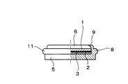
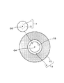
図6は電子マネー取引などに使用するトークンにコアピースを装着する前の状態を示す平面図、図7は装着後の平面図、図8は装着前のトークンの一部拡大断面図、図9は装着前のトークンの一部拡大平面図、図10は図7A−A線上の拡大断面図である。
【0026】
図1に示すように正方形をしたICチップ1の回路形成面側の表面にポリイミド樹脂などからなる絶縁層2を介してスパイラル状のアンテナコイル3が一体に形成されている。アンテナコイル3は電気鋳造メッキ法やフォトレジスト法などにより形成することができ、両端が絶縁層2に形成されたスルーホールを通して入出力端子4、4に接続されている。同図に示すように、ICチップ1の中心O1と、矩形スパイラル状のアンテナコイル3の巻回中心O2が一致するようにアンテナコイル3がICチップ1上に形成されている。
【0027】
コアピース本体5は略カップ状をしており、ポリカーボネート樹脂やエポキシ樹脂などの熱可塑性樹脂で成形され、図2と図3に示すように中央位置に円形で有底状の凹部6を有し、凹部6の開口部周辺に起立したかしめ代7が一体に形成されている。必要に応じてかしめ代7の周方向に1つまたは複数個のV字形あるいはU字形の切欠部を形成することもできる。コアピース本体5の外周面に、断面形状が半円形、三角形、台形などの環状リブ8が1条または複数条形成されている。
【0028】
凹部6の直径D(図2参照)は図1に示すICチップ1の対角線の長さLと略等しく設計され、ICチップ1を凹部6内に挿入することにより、アンテナコイル3の巻回中心O2とコアピース本体5の中心O3が一致するように、すなわちコアピース本体5内でアンテナコイル3(ICチップ1)が中心に自動的に位置決めされるようになっている。
【0029】
ICチップ1はアンテナコイル3側を下にして図5に示すように凹部6内に挿入され、コアピース本体5の上側から超音波溶着ホーン(図示せず)を押し付けてかしめ代7を内側に加熱軟化してかしめ、図4と図5に示すようにICチップ1の4つの角部1a〜1dを係止するかしめ部9を形成して、ICチップ1が凹部6内で固定される。
【0030】
前述のように切欠部を設けることにより、かしめ代7を内側に加熱軟化してかしめる際にしわなどを生じることなく、内側に長く延びたかしめ部9が形成され、外形の小さいICチップ1でもコアピース本体5内に確実に固定できる。またICチップ1はアンテナコイル3側を下にして凹部6内に設置することにより、アンテナコイル3が凹部6の底部12に密着して保護できるから、袋詰やパーツフィーダで供給するときにアンテナコイル3が傷つくことなく、保護効果はある。コアピース本体5を透明または半透明なプラスチックで成形すれば、ICチップ1の装着の有無などの確認ができて便利である。
【0031】
このようにICチップ1をコアピース本体5内に嵌合することにより、コアピース11が構成される。そしてICチップ1をコアピース本体5の凹部6内で担持することにより、アンテナコイル3が保護されるとともに、取り扱い易い大きさにできるから、これをコアピース11として量産し、本来ICチップ1を装着すべき部材にそれぞれ取り付けることができる。特にICチップ1の取扱い時や対象製品と嵌合した後の応力等によるチップ欠けが生じやすいICチップ角部1a〜1dをコアピース11により保護できる。
【0032】
電子マネー取引などに使用するトークン13は例えば直径が30mm、厚さが2.5mmの円板状(コイン状)をしており、内側に配置された非金属製のスペーサ部材14と、そのスペーサ部材14の外周を取り囲む金属製の重量付与部材15の2部材から構成されている。
【0033】
前記スペーサ部材14は、例えばアクリロニトリル−ブタジエン−スチレン樹脂(ABS樹脂)、ポリブチレンテレフタレート樹脂(PBT樹脂)、ポリフェニレンサルファイト樹脂(PPS樹脂)、ポリカーボネート樹脂(PC樹脂)、ポリアミド樹脂、ポリプロピレン樹脂などの合成樹脂の成形体からなる。
【0034】
一方、重量付与部材15を金属単体で構成する場合は、例えばタングステン(比重19.24)、鉛(比重11.34)、ニッケル(比重8.85)、鉄(比重7.86)、アルミニウム(比重2.70)、ステンレス鋼などが用いられる。また、重量付与部材15を金属と合成樹脂の組成物で構成する場合は、例えばタングステン、鉛、ニッケル、鉄、アルミニウム、ステンレス鋼などの金属(粉末状、細片状、繊維状など)と、例えばアクリロニトリル−ブタジエン−スチレン樹脂(ABS樹脂)、ポリブチレンテレフタレート樹脂(PBT樹脂)、ポリフェニレンサルファイト樹脂(PPS樹脂)、ポリカーボネート樹脂(PC樹脂)、ポリアミド樹脂、ポリプロピレン樹脂などの合成樹脂との組成物(混合物)で構成される。
【0035】
金属(粉末状、細片状、繊維状など)の含有率は、約20〜70重量%の範囲が適当である。例えばABS樹脂にタングステンの微粉粉を添加、分散して比重が約3.1の重量付与部材15を構成することができる。
【0036】
前記スペーサ部材14を構成するベース樹脂と重量付与部材15を構成するベース樹脂は、同じでも異なっていてもよい。スペーサ部材14と重量付与部材15のベース樹脂が同じであれば、スペーサ部材14と重量付与部材15の物理的性質が近似しているから、スペーサ部材14と重量付与部材15の接合が確実である。
【0037】
重量付与部材15の中央の透孔に前記スペーサ部材14を強嵌合することにより、重量付与部材15はスペーサ部材14を一体に保持する。
【0038】
このようにトークン13の大部分を金属製の重量付与部材15で構成することにより、トークン13に重量感を付与することができるとともに、落下衝撃などの外力に対してコアピース11とスペーサ部材14の機械的保護に役立つ。
【0039】
スペーサ部材14の中央部には有底状で円形の嵌合部16が設けられ、この嵌合部16の内周面に沿って環状溝部17が形成され、また嵌合部16の底部から上方開口部にかけて空気抜き溝18が1本あるいは複数本(本実施形態では図9に示すように対向するように2本)形成されている。
【0040】
コアピース11は、図6や図7に示すようにトークン13の嵌合部16に強嵌合される。この強嵌合の際に嵌合部16内の空気をある程度逃がさないと、圧縮した空気が嵌合部16内に残り、組み込みが完了したトークンを落下試験したときにコアピース11がトークン13から外れることがある。このようなことを回避するために、嵌合部16の内周面に空気抜き溝18が形成されている。
【0041】
また図10に示すように強嵌合が終了した時点で、コアピース本体5の環状リブ8が嵌合部16の環状溝部17に嵌合するとともに、コアピース本体5の外周面と嵌合部16の内周面とが面で密着する。このときスペーサ部材14がコアピース本体5よりも硬質の合成樹脂で成形しておれば、空気抜き溝18の開口エッジ部10(図9参照)がコアピース本体5の環状リブ8に食い込み、コアピース本体5とトークン13(スペーサ部材14)の結合がより強固になる。
【0042】
図10に示すようにコアピース本体5の底部12が表側になるように、すなわちアンテナコイル3ができるだけ表に近づくように装着され、底部12の表面がトークン13の表面から突出しないように固定される。またこのアンテナコイル3は合成樹脂製のスペーサ部材14を介して金属製重量付与部材15と所定の距離離間している。
【0043】
前述のようにトークン13の中央位置には嵌合部16が形成されているから、結局、ICチップ1の向きは任意であってトークン13の中心O4とICチップ1の中心O2が一致することになる(図6,図7参照)。
【0044】
図11ないし図13は本発明の第2の実施形態に係る非接触通信式情報担体を説明するための図で、図11は重量付与部材の中央部の一部断面図、図12はその重量付与部材にスペーサ部材を強嵌合した状態を示す断面図、図13はそのスペーサ部材の内側にコアピースを強嵌合した状態を示す断面図である。
【0045】
この実施形態で前記第1の実施形態と相違する点は、重量付与部材15の中央部に形成されている透孔19の内周面に沿って断面形状が半円状、三角形状あるいは台形状などの係止リブ20が1条あるいは複数条(本実施形態では断面形状が半円状で1条)の形成されている点である。このように係止リブ20を設けることにより、重量付与部材15にスペーサ部材14を強嵌合した際、図13に示すように係止リブ20が合成樹脂製スペーサ部材14の外周部に食い込み、スペーサ部材14と重量付与部材15の結合がより緊密になる。
【0046】
前記第1の実施形態と第2の実施形態では、重量付与部材15にスペーサ部材14を強嵌合した後に、スペーサ部材14にコアピース11を強嵌合したが、予めスペーサ部材14にコアピース11を強嵌合した後に、そのスペーサ部材14を重量付与部材15に強嵌合しても構わない。
【0047】
図14と図15は本発明の第3の実施形態に係る非接触通信式情報担体を説明するための図で、図14はトークンの中央部の一部断面図、図15はそのトークンの内側にコアピースを嵌合した状態を示す断面図である。
【0048】
この実施形態で前記第1の実施形態と相違する主な点は、スペーサ部材14と重量付与部材15が例えばエポキシ系接着剤やポリアミド系接着剤などの接着剤21で一体化されている点である。本実施形態の場合、スペーサ部材14の外周部に環状溝などの接着剤溜めを設けることもできる。
【0049】
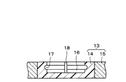
図16ないし図18は本発明の第4の実施形態に係る非接触通信式情報担体を説明するための図で、図16は重量付与部材の中央部の一部断面図、図17はその重量付与部材にスペーサ部材をインサートモールドした状態を示す断面図、図18はそのスペーサ部材の内側にコアピースを強嵌合した状態を示す断面図である。
【0050】
この実施形態で前記第1の実施形態と相違する第1の点は、所定の形状に形成された金属製の重量付与部材15を成形金型に装着して、重量付与部材15の中央部に設けられた透孔19(図16参照)内に合成樹脂製のスペーサ部材14をインサート成形した点である(図17参照)。
【0051】
第2の相違点は、コアピース11の外周面には環状リブ8は設けられておらず、コアピース11の外周面がスペーサ部材14の内周面に密着するか、あるいは接着剤で一体化している点である。
【0052】
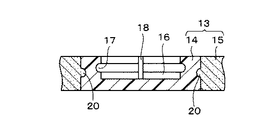
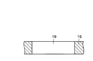
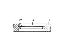
図19ないし図21は本発明の第5の実施形態に係る非接触通信式情報担体を説明するための図で、図19は重量付与部材の中央部の一部断面図、図20はその重量付与部材にスペーサ部材をインサートモールドした状態を示す断面図、図21はそのスペーサ部材の内側にコアピースを強嵌合した状態を示す断面図である。
【0053】
この実施形態で前記第4の実施形態と相違する点は、重量付与部材15の透孔19の内周面に沿って断面形状が凸状、半円状、三角形状あるいは台形状などの係止リブ20が1条あるいは複数条(本実施形態では断面形状が凸状で1条)形成されている点である。このように係止リブ20を設けることにより、重量付与部材15にスペーサ部材14をインサートモールドした際、図20に示すように係止リブ20が合成樹脂製スペーサ部材14の外周部に食い込んだ形になり、スペーサ部材14と重量付与部材15の結合がより緊密になる。
【0054】
図22は本発明の第6の実施形態に係る非接触通信式情報担体を説明するための断面図で、スペーサ部材にコアピースを強嵌合する前の状態を示している。
【0055】
この実施形態の場合も重量付与部材15の透孔19内にスペーサ部材14をインサート成形するが、コアピース11が挿入される側と反対側の透孔19の開口縁に、径方向内側に突出した抜け止めリブ22が周方向に連続的にあるいは断続的に設けられている点である。
【0056】
このように抜け止めリブ22を設けた重量付与部材15にスペーサ部材14をインサート成形しておけば、図22に示すようにスペーサ部材14の内側にコアピース11を瞬間的に強嵌合する際に、スペーサ部材14が重量付与部材15から抜けることが確実に防止できる。
【0057】
図23は本発明の第7の実施形態に係る非接触通信式情報担体を説明するための断面図で、スペーサ部材にコアピースを強嵌合する前の状態を示している。
【0058】
この実施形態で前記第6の実施形態と相違する点は、抜け止めリブ22の代わりに、コアピース11の挿入方向に沿って徐々に径小になったテーパ部23を設けた点である
このようにコアピース11の挿入方向に沿って徐々に径小になったテーパ部23を設けることにより、スペーサ部材14の抜け止めが図れるとともに、コアピース11の強嵌合時に押圧力を利用してスペーサ部材14の外周面が重量付与部材15のテーパ部23により密着することができる。
【0059】
図24は本発明に係る非接触通信式情報担体31とリーダライタ32とホストコンピュータ44の間におけるデータ伝送システムを示すブロック図である。情報担体31はアンテナコイル3、電源生成回路33、メモリ34、コントロール回路35などから構成されている。リーダライタ32は情報担体31側のアンテナコイル3と対応するアンテナコイル36、トランシーバ/レシーバ37、コントローラ38などを備えている。各部の接続は図に示すような関係になっている。
【0060】
図25は情報担体31のアンテナコイル3とリーダライタ32のアンテナコイル36の対応関係を示す図である。アンテナコイル36は、アンテナコイル3の外形と略同じ程度の下面を有する円柱状のフェライトコア39の周面に巻回されている。そしてアンテナコイル3の平面に対してフェライトコア39の軸方向が垂直に配置され、フェライトコア39の下面がアンテナコイル3に近接する。
【0061】
リーダライタ32に装着されるトークン13は、ガイド手段(図示せず)によりトークン13の中心(アンテナコイル3の中心)がフェライトコア39の下面の中心と一致するように位置決めされるから、トークン13(アンテナコイル3)がその平面上においてどのような向きになっても、アンテナコイル3とアンテナコイル36の間で電磁的に結合され、データの授受がなされる。
【0062】
前記実施形態ではスペーサ部材14の方をコアピース本体5よりも硬質にしたが、反対にコアピース本体5の材料に例えばポリフェニレンサルファイト樹脂(PPS樹脂)やポリエーテルイミロ樹脂(PEI樹脂)等のスーパーエンジニアニングプラスチックを使用し、スペーサ部材14の材料にABS樹脂を使用して、コアピース本体5の方をスペーサ部材14りも硬質にすることもできる。
【0063】
このようにすれば、スペーサ部材14の嵌合部16へコアピース11を嵌合する際、あるいは嵌合後の使用時においてコアピース本体5に応力が加わっても、ICチップ1を保護し、チップ割れやICチップの回路破壊を回避することが可能となる。
【0064】
前記実施形態ではコアピース本体5側に環状リブ8を設け、スペーサ部材14側に環状溝部17を形成したが、コアピース本体5側に環状溝部17を形成し、スペーサ部材14側に環状リブ8を設けることもできる。
【0065】
前記実施形態ではスペーサ部材14に有底状の凹部からなる嵌合部16を形成したが、スペーサ部材の上面から下面に貫通した透孔状の嵌合部を設けることもできる。
【0066】
前記実施形態ではスペーサ部材14側に空気抜き溝18を形成したが、コアピース本体5側に空気抜き溝を形成することもできる。
【0067】
本発明に係る非接触通信式情報担体は前記実施形態に記載したトークンの他にカード、DNAチップ,試験菅,検査片などの各種検査対象物を収納するケース、PCカード規格やコンパクトフラッシュ(登録商標)規格等の電子カードのコネクタ部,フレーム部,ケース部、ペン型ポインティングデバイスの先端部、LANケーブルや光ケーブルの接合コネクタ部、自動車等のキー、光ディスク,磁気ディスク,テープ媒体のケースや媒体自身等、今まで適用不可能な小さい領域への装着を実現することが可能となる。
【0068】
【発明の効果】
本発明は、アンテナコイルを一体に形成したICチップを樹脂部材内に装着することにより、コイル形成面の保護ができ、また重量付与部材により非接触通信式情報担体の重量感が増し、取扱性ならびに生産性が良好で安価な非接触通信式情報担体を提供することができる。
【図面の簡単な説明】
【図1】本発明の第1の実施形態に係る非接触通信式情報担体用ICチップの拡大斜視図である。
【図2】コアピース本体の平面図である。
【図3】コアピース本体の一部を切断した正面図である。
【図4】コアピースの平面図である。
【図5】コアピースの一部を切断した正面図である。
【図6】トークンにコアピースを装着する前の状態を示す平面図である。
【図7】トークンにコアピースを装着した後の平面図である。
【図8】装着前のトークンの一部拡大断面図である。
【図9】装着前のトークンの一部拡大平面図である。
【図10】図7A−A線上の拡大断面図である。
【図11】本発明の第2の実施形態に係る非接触通信式情報担体に用いる重量付与部材の中央部の一部断面図である。
【図12】その重量付与部材にスペーサ部材を強嵌合した状態を示す断面図である。
【図13】そのスペーサ部材の内側にコアピースを強嵌合した状態を示す断面図である。
【図14】本発明の第3の実施形態に係る非接触通信式情報担体に用いるトークンの中央部の一部断面図である。
【図15】そのトークンの内側にコアピースを強嵌合した状態を示す断面図である。
【図16】本発明の第4の実施形態に係る非接触通信式情報担体に用いる重量付与部材の中央部の一部断面図である。
【図17】その重量付与部材にスペーサ部材をインサートモールドした状態を示す断面図である。
【図18】そのスペーサ部材の内側にコアピースを強嵌合した状態を示す断面図である。
【図19】本発明の第5の実施形態に係る非接触通信式情報担体に用いる重量付与部材の中央部の一部断面図である。
【図20】その重量付与部材にスペーサ部材をインサートモールドした状態を示す断面図である。
【図21】そのスペーサ部材の内側にコアピースを強嵌合した状態を示す断面図である。
【図22】本発明の第6の実施形態に係る非接触通信式情報担体のスペーサ部材にコアピースを強嵌合する前の状態を示す断面図である。
【図23】本発明の第7の実施形態に係る非接触通信式情報担体のスペーサ部材にコアピースを強嵌合する前の状態を示す断面図である。
【図24】本発明に係る非接触通信式情報担体とリーダライタとホストコンピュータの間におけるデータ伝送システムを示すブロック図である。
【図25】非接触通信式情報担体のアンテナコイルとリーダライタのアンテナコイルの対応関係を示す図である。
【図26】従来提案されたコイン形ICタグを説明するための断面図である。
【符号の説明】
1 ICチップ
1a〜1d ICチップの角部
3 アンテナコイル
5 コアピース本体
6 凹部
7 かしめ代
8 環状リブ
9 かしめ部
10 開口エッジ部
11 コアピース
12 底部
13 トークン
14 スペーサ部材
15 重量付与部材
16 嵌合部
17 環状溝部
18 空気抜き溝
19 透孔
20 係止リブ
21 接着剤
22 抜け止めリブ
D コアピス本体の凹部の直径
L ICチップの対角線の長さ
O1 ICチップの中心
O2 アンテナコイルの巻回中心
O3 コアピス本体の中心
O4 トークンの中心[0001]
BACKGROUND OF THE INVENTION
The present invention relates to a non-contact communication type information carrier including a semiconductor device in which a non-contact communication antenna is integrally formed on an IC chip.
[0002]
[Prior art]
Conventionally, for example, for inventory management of parts and products, an antenna chip is used to attach an IC chip integrally formed with an antenna coil to parts or products, or to use for applications such as entrance / exit management and commuter passes. There has been proposed a personal identification card in which an IC chip integrally formed with a coil is embedded in a card body.
[0003]
[Problems to be solved by the invention]
However, the IC chip with the integrated antenna coil is hard, and if the IC chips come into contact with each other, the coil forming surface is easily damaged. Therefore, the IC chip cannot be packaged or supplied by a parts feeder, and it is necessary to rely on expensive material handling. Absent.
[0004]
In addition, an IC chip integrally formed with an antenna coil is extremely thin (thickness is about 0.2 mm to 0.6 mm) and has high brittleness, so that cracking or chipping due to stress occurs on the coil forming surface side (or the back surface side). It is easy and secondary processing is difficult.
[0005]
In addition, insert molding of chips using synthetic resin is possible, but because the difference in physical characteristics between the IC chip and the molded resin formed integrally with the antenna coil is large, the moldability is poor, and it is difficult to take many pieces. It has drawbacks such as high costs.
[0006]
In addition, when insert molding is performed, thermal expansion due to the embedded resin and stress strain generated during use directly affect the IC chip, and in the worst case, the IC chip is destroyed.
[0007]
Conventionally, a coin-type IC tag as described in, for example, JP-A-2002-7989 has been proposed. As shown in FIG. 26, this coin-shaped IC tag is formed by applying a
[0008]
On the other hand, the
[0009]
By using the two
[0010]
However, when the coin-shaped IC tag is integrated with the
[0011]
In addition, the
[0012]
An object of the present invention is to provide a non-contact communication type information carrier that eliminates such drawbacks of the prior art and has good handleability and productivity.
[0013]
[Means for Solving the Problems]
In order to achieve the above object, a first means of the present invention surrounds an IC chip in which an antenna coil for non-contact communication is formed on one surface, a non-metallic resin member that houses the IC chip, and the resin member. Thus, at least a part or all of the arrangement / connection is made of a weight imparting member made of metal .
[0014]
According to a second means of the present invention, in the first means, the weight imparting member is made of a composition of a metal and a synthetic resin .
[0015]
According to a third means of the present invention, in the first means, the non-contact communication type information carrier has a coin shape, and the IC chip is built in the center position of the non-contact communication type information carrier. It is what.
[0024]
DETAILED DESCRIPTION OF THE INVENTION
Hereinafter, embodiments of the present invention will be described with reference to the drawings. 1 to 10 are diagrams for explaining a non-contact communication type information carrier according to the first embodiment. FIG. 1 is an enlarged perspective view of an IC chip, FIG. 2 is a plan view of a core piece body, and FIG. 3 is a core piece. FIG. 4 is a plan view of the core piece, and FIG. 5 is a front view of the core piece cut away.
[0025]
6 is a plan view showing a state before a core piece is attached to a token used for electronic money transactions, etc., FIG. 7 is a plan view after attachment, FIG. 8 is a partially enlarged sectional view of the token before attachment, and FIG. FIG. 10 is a partially enlarged plan view of the token before being mounted, and FIG.
[0026]
As shown in FIG. 1, a
[0027]
The
[0028]
The diameter D (see FIG. 2) of the
[0029]
The
[0030]
By providing the notch portion as described above, the
[0031]
By fitting the
[0032]
The token 13 used for electronic money transactions or the like has a disk shape (coin shape) having a diameter of 30 mm and a thickness of 2.5 mm, for example, and a
[0033]
The
[0034]
On the other hand, when the
[0035]
The content of metal (powder, strip, fiber, etc.) is suitably in the range of about 20 to 70% by weight. For example, a
[0036]
The base resin constituting the
[0037]
By strongly fitting the
[0038]
As described above, most of the token 13 is configured by the metal
[0039]
A bottomed circular
[0040]
The
[0041]
Further, as shown in FIG. 10, when the strong fitting is finished, the
[0042]
As shown in FIG. 10, the
[0043]
Since the
[0044]
11 to 13 are views for explaining a non-contact communication type information carrier according to the second embodiment of the present invention. FIG. 11 is a partial cross-sectional view of the central portion of the weight applying member, and FIG. FIG. 13 is a cross-sectional view showing a state in which the spacer member is strongly fitted to the applying member, and FIG. 13 is a cross-sectional view showing a state in which the core piece is strongly fitted inside the spacer member.
[0045]
This embodiment is different from the first embodiment in that the cross-sectional shape is semicircular, triangular or trapezoidal along the inner peripheral surface of the through
[0046]
In the first embodiment and the second embodiment, after the
[0047]
14 and 15 are diagrams for explaining a non-contact communication type information carrier according to the third embodiment of the present invention. FIG. 14 is a partial sectional view of a central portion of the token, and FIG. 15 is an inner side of the token. It is sectional drawing which shows the state which fitted the core piece to.
[0048]
In this embodiment, the main difference from the first embodiment is that the
[0049]
16 to 18 are views for explaining a non-contact communication type information carrier according to the fourth embodiment of the present invention. FIG. 16 is a partial cross-sectional view of the central portion of the weight applying member, and FIG. FIG. 18 is a cross-sectional view showing a state where the spacer member is insert-molded to the applying member, and FIG. 18 is a cross-sectional view showing a state where the core piece is strongly fitted inside the spacer member.
[0050]
In this embodiment, the first point different from the first embodiment is that a metal
[0051]
The second difference is that the outer peripheral surface of the
[0052]
19 to 21 are views for explaining a non-contact communication type information carrier according to the fifth embodiment of the present invention. FIG. 19 is a partial cross-sectional view of the central portion of the weight imparting member, and FIG. FIG. 21 is a cross-sectional view showing a state where the spacer member is insert-molded on the applying member, and FIG. 21 is a cross-sectional view showing a state where the core piece is strongly fitted inside the spacer member.
[0053]
This embodiment differs from the fourth embodiment in that the cross-sectional shape is convex, semicircular, triangular or trapezoidal along the inner peripheral surface of the through
[0054]
FIG. 22 is a sectional view for explaining the non-contact communication type information carrier according to the sixth embodiment of the present invention, and shows a state before the core piece is strongly fitted to the spacer member.
[0055]
Also in this embodiment, the
[0056]
If the
[0057]
FIG. 23 is a cross-sectional view for explaining a non-contact communication type information carrier according to the seventh embodiment of the present invention, and shows a state before the core piece is strongly fitted to the spacer member.
[0058]
This embodiment is different from the sixth embodiment in that a tapered
[0059]
FIG. 24 is a block diagram showing a data transmission system among the non-contact communication
[0060]
FIG. 25 is a diagram showing a correspondence relationship between the
[0061]
The token 13 attached to the reader /
[0062]
In the above embodiment, the
[0063]
In this way, even when the
[0064]
In the embodiment, the
[0065]
In the above-described embodiment, the
[0066]
In the embodiment, the
[0067]
The non-contact communication type information carrier according to the present invention is a case for storing various test objects such as a card, a DNA chip, a test cage, and a test piece in addition to the token described in the above embodiment, a PC card standard and a compact flash (registered) Trademark) standard electronic card connector part, frame part, case part, tip part of pen-type pointing device, joint connector part of LAN cable or optical cable, key of automobile etc., optical disk, magnetic disk, tape medium case and medium It is possible to realize mounting on a small area that cannot be applied until now.
[0068]
【The invention's effect】
In the present invention , by mounting an IC chip integrally formed with an antenna coil in a resin member , the coil forming surface can be protected, and the weight imparting member increases the feeling of weight of the non-contact communication type information carrier , so that handling is easy. In addition, it is possible to provide an inexpensive non-contact communication type information carrier with good productivity.
[Brief description of the drawings]
FIG. 1 is an enlarged perspective view of an IC chip for non-contact communication type information carrier according to a first embodiment of the present invention.
FIG. 2 is a plan view of a core piece body.
FIG. 3 is a front view in which a part of the core piece body is cut.
FIG. 4 is a plan view of a core piece.
FIG. 5 is a front view in which a part of the core piece is cut.
FIG. 6 is a plan view showing a state before a core piece is attached to a token.
FIG. 7 is a plan view after the core piece is mounted on the token.
FIG. 8 is a partially enlarged cross-sectional view of the token before mounting.
FIG. 9 is a partially enlarged plan view of the token before mounting.
FIG. 10 is an enlarged cross-sectional view taken along line 7A-A in FIG.
FIG. 11 is a partial cross-sectional view of a central portion of a weight imparting member used for a non-contact communication type information carrier according to a second embodiment of the present invention.
FIG. 12 is a cross-sectional view showing a state in which a spacer member is strongly fitted to the weight imparting member.
FIG. 13 is a cross-sectional view showing a state in which a core piece is strongly fitted inside the spacer member.
FIG. 14 is a partial cross-sectional view of a central portion of a token used in a non-contact communication type information carrier according to a third embodiment of the present invention.
FIG. 15 is a cross-sectional view showing a state in which a core piece is strongly fitted inside the token.
FIG. 16 is a partial cross-sectional view of a central portion of a weight imparting member used for a non-contact communication type information carrier according to a fourth embodiment of the present invention.
FIG. 17 is a cross-sectional view showing a state in which a spacer member is insert-molded to the weight imparting member.
FIG. 18 is a cross-sectional view showing a state in which a core piece is strongly fitted inside the spacer member.
FIG. 19 is a partial cross-sectional view of a central portion of a weight imparting member used in a non-contact communication type information carrier according to a fifth embodiment of the present invention.
FIG. 20 is a cross-sectional view showing a state in which a spacer member is insert-molded to the weight imparting member.
FIG. 21 is a cross-sectional view showing a state in which a core piece is strongly fitted inside the spacer member.
FIG. 22 is a cross-sectional view showing a state before a core piece is strongly fitted to a spacer member of a non-contact communication type information carrier according to a sixth embodiment of the present invention.
FIG. 23 is a cross-sectional view showing a state before the core piece is strongly fitted to the spacer member of the non-contact communication type information carrier according to the seventh embodiment of the present invention.
FIG. 24 is a block diagram showing a data transmission system among a contactless communication type information carrier, a reader / writer, and a host computer according to the present invention.
FIG. 25 is a diagram showing a correspondence relationship between an antenna coil of a non-contact communication type information carrier and an antenna coil of a reader / writer.
FIG. 26 is a cross-sectional view for explaining a conventionally proposed coin-shaped IC tag.
[Explanation of symbols]
1
Claims (3)
前記ICチップを内装する非金属製の樹脂部材と、
前記樹脂部材を取り囲むように配置・連結された少なくとも一部または全部が金属からなる重量付与部材から構成されていることを特徴とする非接触通信式情報担体。An IC chip in which an antenna coil for non-contact communication is formed on one surface;
A non-metallic resin member that houses the IC chip;
A non-contact communication type information carrier characterized in that at least a part or all of the resin member is arranged and connected so as to surround the resin member, and is composed of a weight imparting member made of metal.
Priority Applications (5)
| Application Number | Priority Date | Filing Date | Title |
|---|---|---|---|
| JP2002176270A JP4143340B2 (en) | 2002-06-17 | 2002-06-17 | Non-contact communication type information carrier |
| CNB03813991XA CN100339866C (en) | 2002-06-17 | 2003-06-17 | Non-contact communication system information carrier |
| AU2003244144A AU2003244144A1 (en) | 2002-06-17 | 2003-06-17 | Non-contact communication system information carrier |
| PCT/JP2003/007678 WO2003107268A1 (en) | 2002-06-17 | 2003-06-17 | Non-contact communication system information carrier |
| US10/518,299 US7327266B2 (en) | 2002-06-17 | 2003-06-17 | Non-contact communication system information carrier |
Applications Claiming Priority (1)
| Application Number | Priority Date | Filing Date | Title |
|---|---|---|---|
| JP2002176270A JP4143340B2 (en) | 2002-06-17 | 2002-06-17 | Non-contact communication type information carrier |
Related Child Applications (1)
| Application Number | Title | Priority Date | Filing Date |
|---|---|---|---|
| JP2004147655A Division JP3591652B2 (en) | 2004-05-18 | 2004-05-18 | Non-contact communication information carrier |
Publications (3)
| Publication Number | Publication Date |
|---|---|
| JP2004021649A JP2004021649A (en) | 2004-01-22 |
| JP2004021649A5 JP2004021649A5 (en) | 2005-04-07 |
| JP4143340B2 true JP4143340B2 (en) | 2008-09-03 |
Family
ID=29728088
Family Applications (1)
| Application Number | Title | Priority Date | Filing Date |
|---|---|---|---|
| JP2002176270A Expired - Fee Related JP4143340B2 (en) | 2002-06-17 | 2002-06-17 | Non-contact communication type information carrier |
Country Status (5)
| Country | Link |
|---|---|
| US (1) | US7327266B2 (en) |
| JP (1) | JP4143340B2 (en) |
| CN (1) | CN100339866C (en) |
| AU (1) | AU2003244144A1 (en) |
| WO (1) | WO2003107268A1 (en) |
Families Citing this family (19)
| Publication number | Priority date | Publication date | Assignee | Title |
|---|---|---|---|---|
| WO2002075646A1 (en) * | 2001-03-19 | 2002-09-26 | Hitachi Maxell, Ltd. | Core piece and non-contact communication type information carrier using the core piece |
| JP4596844B2 (en) * | 2004-07-23 | 2010-12-15 | テルモ株式会社 | Medical article and ordering system for medical article |
| US20060276157A1 (en) * | 2005-06-03 | 2006-12-07 | Chen Zhi N | Apparatus and methods for packaging antennas with integrated circuit chips for millimeter wave applications |
| US8346382B2 (en) | 2005-08-25 | 2013-01-01 | Coldtrack, Llc | Hierarchical sample storage system |
| US7973664B1 (en) * | 2006-08-04 | 2011-07-05 | Rexam Healthcare Packaging Inc. | Closure having RFID and foil |
| US8996210B2 (en) * | 2008-01-17 | 2015-03-31 | Sea-Watch Technologies, Inc. | Integrated vessel monitoring and control system |
| US20090267767A1 (en) * | 2008-04-24 | 2009-10-29 | Chris Chen | Radio Frequency Identification Tag for a Mobile Phone |
| JP5304349B2 (en) * | 2009-03-12 | 2013-10-02 | 大日本印刷株式会社 | Method for manufacturing metal article with IC tag, metal article with IC tag |
| DE102009015579A1 (en) * | 2009-03-30 | 2010-10-07 | Soheil Hamedani | Coin with integrated RFID identification device and method for its production |
| US8164456B2 (en) * | 2009-04-06 | 2012-04-24 | Toyota Motor Engineering & Manufacturing North America, Inc. | Device for incrementally adjusting the position of an RFID tag |
| KR20110018777A (en) * | 2009-08-18 | 2011-02-24 | 삼성엘이디 주식회사 | Light emitting diode package |
| US8872627B2 (en) | 2010-02-12 | 2014-10-28 | Biotillion, Llc | Tracking biological and other samples using RFID tags |
| US9431692B2 (en) | 2011-04-07 | 2016-08-30 | Biotillion, Llc | Tracking biological and other samples using RFID tags |
| US9714730B2 (en) * | 2011-09-02 | 2017-07-25 | Vallourec Oil And Gas France | Identification tags and systems suitable for thin-walled components |
| CN103999287B (en) * | 2012-09-18 | 2016-11-16 | 松下知识产权经营株式会社 | Antenna, dispensing device, reception device, three dimensional integrated circuits and non-contact communication system |
| CN105048060A (en) * | 2015-07-23 | 2015-11-11 | 爱康普科技(大连)有限公司 | Anti-interference antenna for radio frequency identification (RFID) tag reader |
| JP6841135B2 (en) * | 2017-04-10 | 2021-03-10 | 凸版印刷株式会社 | Coin-shaped IC tag and its manufacturing method |
| RU2706655C1 (en) * | 2019-01-28 | 2019-11-19 | Акционерное общество "Гознак" (АО "Гознак") | Polymer-containing composite protected article |
| US12006126B2 (en) | 2019-09-03 | 2024-06-11 | Bio Tillion, Llc | Techniques for tracking physical parameters such as temperature of transported biological materials |
Family Cites Families (14)
| Publication number | Priority date | Publication date | Assignee | Title |
|---|---|---|---|---|
| DE2825962C2 (en) * | 1978-06-14 | 1987-04-16 | Akzo Gmbh, 5600 Wuppertal | Lubricants for the forming processing of thermoplastics |
| JPH0550790A (en) * | 1991-08-26 | 1993-03-02 | Matsushita Electric Ind Co Ltd | Information medium |
| EP0704092A1 (en) | 1994-04-18 | 1996-04-03 | Gay Frères Vente et Exportation S.A. | Electronic memory device |
| FR2723228B1 (en) * | 1994-07-26 | 1996-09-20 | Bourgogne Grasset | IMPROVED GAME TOKEN |
| WO1998039989A1 (en) | 1997-03-10 | 1998-09-17 | Etablissements Bourgogne Et Grasset | Token with electronic chip |
| EP0952542B1 (en) * | 1997-06-23 | 2003-10-29 | Rohm Co., Ltd. | Ic module and ic card |
| US5982284A (en) * | 1997-09-19 | 1999-11-09 | Avery Dennison Corporation | Tag or label with laminated thin, flat, flexible device |
| SG91249A1 (en) * | 1999-01-14 | 2002-09-17 | Lintec Corp | Process for producing non-contact data carrier |
| JP3534042B2 (en) * | 2000-06-21 | 2004-06-07 | オムロン株式会社 | Coin-shaped IC tag and method of manufacturing the same |
| JP3711026B2 (en) * | 2000-07-17 | 2005-10-26 | 株式会社ハネックス | RFID tag installation structure, RFID tag installation method, and RFID tag communication method |
| DE60135855D1 (en) * | 2000-07-19 | 2008-10-30 | Hanex Co Ltd | RFID LABEL CASE STRUCTURE, RFID LABEL INSTALLATION STRUCTURE AND RFID LABEL COMMUNICATION PROCEDURES |
| JP3481575B2 (en) * | 2000-09-28 | 2003-12-22 | 寛児 川上 | antenna |
| TW531976B (en) * | 2001-01-11 | 2003-05-11 | Hanex Co Ltd | Communication apparatus and installing structure, manufacturing method and communication method |
| JP3554295B2 (en) * | 2001-06-29 | 2004-08-18 | 株式会社マースエンジニアリング | Enhanced contactless data carrier and method of manufacturing the same |
-
2002
- 2002-06-17 JP JP2002176270A patent/JP4143340B2/en not_active Expired - Fee Related
-
2003
- 2003-06-17 WO PCT/JP2003/007678 patent/WO2003107268A1/en active Application Filing
- 2003-06-17 AU AU2003244144A patent/AU2003244144A1/en not_active Abandoned
- 2003-06-17 CN CNB03813991XA patent/CN100339866C/en not_active Expired - Fee Related
- 2003-06-17 US US10/518,299 patent/US7327266B2/en not_active Expired - Fee Related
Also Published As
| Publication number | Publication date |
|---|---|
| WO2003107268A1 (en) | 2003-12-24 |
| JP2004021649A (en) | 2004-01-22 |
| US20060016895A1 (en) | 2006-01-26 |
| AU2003244144A1 (en) | 2003-12-31 |
| CN1662927A (en) | 2005-08-31 |
| CN100339866C (en) | 2007-09-26 |
| US7327266B2 (en) | 2008-02-05 |
Similar Documents
| Publication | Publication Date | Title |
|---|---|---|
| JP4143340B2 (en) | Non-contact communication type information carrier | |
| US6687131B1 (en) | Transponder and injection-molded part and method for manufacturing same | |
| US7926725B2 (en) | Method of making a token with an electronic identifier | |
| US6851618B2 (en) | Contactless or hybrid contact-contactless smart card with reinforced connection of the electronic module | |
| US7942334B2 (en) | Token with an electronic identifier | |
| US20100320270A1 (en) | Combi card and communication system using thereof | |
| JPH0852968A (en) | Non-contact card and its production | |
| EP0488574A2 (en) | Personal data card construction | |
| EP0326822A2 (en) | Data device module | |
| JP4028763B2 (en) | Non-contact communication type information carrier | |
| JP3591652B2 (en) | Non-contact communication information carrier | |
| JP4028764B2 (en) | Non-contact communication type information carrier | |
| US7159785B2 (en) | Core piece and non-contact communication type information carrier using the core piece | |
| JP4680567B2 (en) | Coin type recording medium | |
| JPH11219418A (en) | Ic card to be used as both of contact type and non contact type | |
| JP2005222277A (en) | Information recording medium | |
| JP3876174B2 (en) | Non-contact communication type information carrier | |
| JP3464795B1 (en) | Core piece for non-contact communication type information carrier | |
| CN117063181A (en) | Chip card and method for producing a chip card | |
| GB2312089A (en) | Contactless data carrier | |
| JP4854885B2 (en) | Non-contact communication type information carrier and information processing system using the same | |
| JP4705726B2 (en) | Core piece for non-contact communication type information carrier | |
| JP2009110143A (en) | Coin-shaped rfid tag | |
| JP2001229360A (en) | Ic card | |
| JP4459670B2 (en) | UIM with plate frame |
Legal Events
| Date | Code | Title | Description |
|---|---|---|---|
| A521 | Written amendment |
Free format text: JAPANESE INTERMEDIATE CODE: A523 Effective date: 20040518 |
|
| A621 | Written request for application examination |
Free format text: JAPANESE INTERMEDIATE CODE: A621 Effective date: 20041117 |
|
| TRDD | Decision of grant or rejection written | ||
| A01 | Written decision to grant a patent or to grant a registration (utility model) |
Free format text: JAPANESE INTERMEDIATE CODE: A01 Effective date: 20080603 |
|
| A01 | Written decision to grant a patent or to grant a registration (utility model) |
Free format text: JAPANESE INTERMEDIATE CODE: A01 |
|
| A61 | First payment of annual fees (during grant procedure) |
Free format text: JAPANESE INTERMEDIATE CODE: A61 Effective date: 20080616 |
|
| FPAY | Renewal fee payment (event date is renewal date of database) |
Free format text: PAYMENT UNTIL: 20110620 Year of fee payment: 3 |
|
| R150 | Certificate of patent or registration of utility model |
Free format text: JAPANESE INTERMEDIATE CODE: R150 |
|
| FPAY | Renewal fee payment (event date is renewal date of database) |
Free format text: PAYMENT UNTIL: 20110620 Year of fee payment: 3 |
|
| FPAY | Renewal fee payment (event date is renewal date of database) |
Free format text: PAYMENT UNTIL: 20110620 Year of fee payment: 3 |
|
| FPAY | Renewal fee payment (event date is renewal date of database) |
Free format text: PAYMENT UNTIL: 20120620 Year of fee payment: 4 |
|
| FPAY | Renewal fee payment (event date is renewal date of database) |
Free format text: PAYMENT UNTIL: 20120620 Year of fee payment: 4 |
|
| FPAY | Renewal fee payment (event date is renewal date of database) |
Free format text: PAYMENT UNTIL: 20130620 Year of fee payment: 5 |
|
| FPAY | Renewal fee payment (event date is renewal date of database) |
Free format text: PAYMENT UNTIL: 20130620 Year of fee payment: 5 |
|
| FPAY | Renewal fee payment (event date is renewal date of database) |
Free format text: PAYMENT UNTIL: 20130620 Year of fee payment: 5 |
|
| R250 | Receipt of annual fees |
Free format text: JAPANESE INTERMEDIATE CODE: R250 |
|
| LAPS | Cancellation because of no payment of annual fees |