EP0948754B1 - Lichtmoduliertes konfokales optisches instrument - Google Patents
Lichtmoduliertes konfokales optisches instrument Download PDFInfo
- Publication number
- EP0948754B1 EP0948754B1 EP97952425.3A EP97952425A EP0948754B1 EP 0948754 B1 EP0948754 B1 EP 0948754B1 EP 97952425 A EP97952425 A EP 97952425A EP 0948754 B1 EP0948754 B1 EP 0948754B1
- Authority
- EP
- European Patent Office
- Prior art keywords
- light
- illumination
- pattern
- confocal
- specimen
- Prior art date
- Legal status (The legal status is an assumption and is not a legal conclusion. Google has not performed a legal analysis and makes no representation as to the accuracy of the status listed.)
- Expired - Lifetime
Links
- 230000003287 optical effect Effects 0.000 title claims description 60
- 238000005286 illumination Methods 0.000 claims description 79
- 238000003384 imaging method Methods 0.000 claims description 34
- 238000010226 confocal imaging Methods 0.000 claims description 13
- 238000012634 optical imaging Methods 0.000 claims description 10
- 230000008878 coupling Effects 0.000 claims description 8
- 238000010168 coupling process Methods 0.000 claims description 8
- 238000005859 coupling reaction Methods 0.000 claims description 8
- 230000005540 biological transmission Effects 0.000 claims description 6
- 230000004044 response Effects 0.000 claims description 5
- 239000000835 fiber Substances 0.000 claims description 2
- 239000004020 conductor Substances 0.000 claims 1
- 238000012360 testing method Methods 0.000 description 22
- 238000000034 method Methods 0.000 description 15
- 238000012545 processing Methods 0.000 description 11
- 238000001514 detection method Methods 0.000 description 10
- 230000005284 excitation Effects 0.000 description 10
- 238000010586 diagram Methods 0.000 description 9
- 238000011160 research Methods 0.000 description 8
- 230000004075 alteration Effects 0.000 description 7
- 230000009977 dual effect Effects 0.000 description 6
- 210000004027 cell Anatomy 0.000 description 5
- 150000001875 compounds Chemical class 0.000 description 5
- 230000001419 dependent effect Effects 0.000 description 5
- 239000003269 fluorescent indicator Substances 0.000 description 5
- 230000010287 polarization Effects 0.000 description 5
- OYPRJOBELJOOCE-UHFFFAOYSA-N Calcium Chemical compound [Ca] OYPRJOBELJOOCE-UHFFFAOYSA-N 0.000 description 4
- XUIMIQQOPSSXEZ-UHFFFAOYSA-N Silicon Chemical compound [Si] XUIMIQQOPSSXEZ-UHFFFAOYSA-N 0.000 description 4
- 238000003491 array Methods 0.000 description 4
- 239000011575 calcium Substances 0.000 description 4
- 229910052791 calcium Inorganic materials 0.000 description 4
- 238000001816 cooling Methods 0.000 description 4
- 238000000386 microscopy Methods 0.000 description 4
- 239000013307 optical fiber Substances 0.000 description 4
- 229910052710 silicon Inorganic materials 0.000 description 4
- 239000010703 silicon Substances 0.000 description 4
- 230000015572 biosynthetic process Effects 0.000 description 3
- 238000004624 confocal microscopy Methods 0.000 description 3
- 238000012937 correction Methods 0.000 description 3
- 210000001519 tissue Anatomy 0.000 description 3
- 210000000349 chromosome Anatomy 0.000 description 2
- 230000000295 complement effect Effects 0.000 description 2
- 238000009826 distribution Methods 0.000 description 2
- 238000005516 engineering process Methods 0.000 description 2
- YFHXZQPUBCBNIP-UHFFFAOYSA-N fura-2 Chemical compound CC1=CC=C(N(CC(O)=O)CC(O)=O)C(OCCOC=2C(=CC=3OC(=CC=3C=2)C=2OC(=CN=2)C(O)=O)N(CC(O)=O)CC(O)=O)=C1 YFHXZQPUBCBNIP-UHFFFAOYSA-N 0.000 description 2
- 230000017525 heat dissipation Effects 0.000 description 2
- 230000003834 intracellular effect Effects 0.000 description 2
- 239000003446 ligand Substances 0.000 description 2
- 230000000873 masking effect Effects 0.000 description 2
- 238000001000 micrograph Methods 0.000 description 2
- 238000006303 photolysis reaction Methods 0.000 description 2
- 230000015843 photosynthesis, light reaction Effects 0.000 description 2
- 238000000926 separation method Methods 0.000 description 2
- 230000002123 temporal effect Effects 0.000 description 2
- 206010021143 Hypoxia Diseases 0.000 description 1
- DGAQECJNVWCQMB-PUAWFVPOSA-M Ilexoside XXIX Chemical compound C[C@@H]1CC[C@@]2(CC[C@@]3(C(=CC[C@H]4[C@]3(CC[C@@H]5[C@@]4(CC[C@@H](C5(C)C)OS(=O)(=O)[O-])C)C)[C@@H]2[C@]1(C)O)C)C(=O)O[C@H]6[C@@H]([C@H]([C@@H]([C@H](O6)CO)O)O)O.[Na+] DGAQECJNVWCQMB-PUAWFVPOSA-M 0.000 description 1
- 206010034972 Photosensitivity reaction Diseases 0.000 description 1
- 238000002679 ablation Methods 0.000 description 1
- 238000010521 absorption reaction Methods 0.000 description 1
- 238000013459 approach Methods 0.000 description 1
- 238000003705 background correction Methods 0.000 description 1
- 210000004556 brain Anatomy 0.000 description 1
- 230000003139 buffering effect Effects 0.000 description 1
- 230000008859 change Effects 0.000 description 1
- 238000002983 circular dichroism Methods 0.000 description 1
- 230000001427 coherent effect Effects 0.000 description 1
- 239000003086 colorant Substances 0.000 description 1
- 230000001010 compromised effect Effects 0.000 description 1
- 238000005094 computer simulation Methods 0.000 description 1
- 239000012141 concentrate Substances 0.000 description 1
- 230000001268 conjugating effect Effects 0.000 description 1
- 230000007423 decrease Effects 0.000 description 1
- 230000007812 deficiency Effects 0.000 description 1
- 230000001627 detrimental effect Effects 0.000 description 1
- 239000003814 drug Substances 0.000 description 1
- 229940079593 drug Drugs 0.000 description 1
- 239000000975 dye Substances 0.000 description 1
- 230000000694 effects Effects 0.000 description 1
- 239000005262 ferroelectric liquid crystals (FLCs) Substances 0.000 description 1
- 238000001914 filtration Methods 0.000 description 1
- 238000000799 fluorescence microscopy Methods 0.000 description 1
- 238000002376 fluorescence recovery after photobleaching Methods 0.000 description 1
- 230000006870 function Effects 0.000 description 1
- 230000001146 hypoxic effect Effects 0.000 description 1
- PNDZEEPOYCVIIY-UHFFFAOYSA-N indo-1 Chemical compound CC1=CC=C(N(CC(O)=O)CC(O)=O)C(OCCOC=2C(=CC=C(C=2)C=2N=C3[CH]C(=CC=C3C=2)C(O)=O)N(CC(O)=O)CC(O)=O)=C1 PNDZEEPOYCVIIY-UHFFFAOYSA-N 0.000 description 1
- 238000007689 inspection Methods 0.000 description 1
- 230000003993 interaction Effects 0.000 description 1
- 238000004519 manufacturing process Methods 0.000 description 1
- 239000000463 material Substances 0.000 description 1
- KJLLKLRVCJAFRY-UHFFFAOYSA-N mebutizide Chemical compound ClC1=C(S(N)(=O)=O)C=C2S(=O)(=O)NC(C(C)C(C)CC)NC2=C1 KJLLKLRVCJAFRY-UHFFFAOYSA-N 0.000 description 1
- 230000001537 neural effect Effects 0.000 description 1
- 210000002569 neuron Anatomy 0.000 description 1
- 239000002858 neurotransmitter agent Substances 0.000 description 1
- 230000002186 photoactivation Effects 0.000 description 1
- 230000008832 photodamage Effects 0.000 description 1
- 208000007578 phototoxic dermatitis Diseases 0.000 description 1
- 231100000018 phototoxicity Toxicity 0.000 description 1
- 239000002243 precursor Substances 0.000 description 1
- 230000008569 process Effects 0.000 description 1
- 238000003908 quality control method Methods 0.000 description 1
- 238000004064 recycling Methods 0.000 description 1
- 238000005070 sampling Methods 0.000 description 1
- DYPYMMHZGRPOCK-UHFFFAOYSA-N seminaphtharhodafluor Chemical compound O1C(=O)C2=CC=CC=C2C21C(C=CC=1C3=CC=C(O)C=1)=C3OC1=CC(N)=CC=C21 DYPYMMHZGRPOCK-UHFFFAOYSA-N 0.000 description 1
- 238000012163 sequencing technique Methods 0.000 description 1
- XJKVPKYVPCWHFO-UHFFFAOYSA-N silicon;hydrate Chemical compound O.[Si] XJKVPKYVPCWHFO-UHFFFAOYSA-N 0.000 description 1
- 239000011734 sodium Substances 0.000 description 1
- 229910052708 sodium Inorganic materials 0.000 description 1
- 239000007787 solid Substances 0.000 description 1
- 125000006850 spacer group Chemical group 0.000 description 1
- 241000894007 species Species 0.000 description 1
- 238000010186 staining Methods 0.000 description 1
- 238000003860 storage Methods 0.000 description 1
- 238000001356 surgical procedure Methods 0.000 description 1
- 230000000946 synaptic effect Effects 0.000 description 1
- 238000012549 training Methods 0.000 description 1
- 238000013519 translation Methods 0.000 description 1
- 230000001960 triggered effect Effects 0.000 description 1
- 235000012431 wafers Nutrition 0.000 description 1
Images


Classifications
-
- G—PHYSICS
- G01—MEASURING; TESTING
- G01M—TESTING STATIC OR DYNAMIC BALANCE OF MACHINES OR STRUCTURES; TESTING OF STRUCTURES OR APPARATUS, NOT OTHERWISE PROVIDED FOR
- G01M11/00—Testing of optical apparatus; Testing structures by optical methods not otherwise provided for
- G01M11/02—Testing optical properties
- G01M11/0242—Testing optical properties by measuring geometrical properties or aberrations
- G01M11/0257—Testing optical properties by measuring geometrical properties or aberrations by analyzing the image formed by the object to be tested
- G01M11/0264—Testing optical properties by measuring geometrical properties or aberrations by analyzing the image formed by the object to be tested by using targets or reference patterns
-
- G—PHYSICS
- G02—OPTICS
- G02B—OPTICAL ELEMENTS, SYSTEMS OR APPARATUS
- G02B21/00—Microscopes
- G02B21/0004—Microscopes specially adapted for specific applications
- G02B21/002—Scanning microscopes
- G02B21/0024—Confocal scanning microscopes (CSOMs) or confocal "macroscopes"; Accessories which are not restricted to use with CSOMs, e.g. sample holders
- G02B21/0036—Scanning details, e.g. scanning stages
- G02B21/004—Scanning details, e.g. scanning stages fixed arrays, e.g. switchable aperture arrays
-
- G—PHYSICS
- G02—OPTICS
- G02B—OPTICAL ELEMENTS, SYSTEMS OR APPARATUS
- G02B21/00—Microscopes
- G02B21/0004—Microscopes specially adapted for specific applications
- G02B21/002—Scanning microscopes
- G02B21/0024—Confocal scanning microscopes (CSOMs) or confocal "macroscopes"; Accessories which are not restricted to use with CSOMs, e.g. sample holders
- G02B21/0036—Scanning details, e.g. scanning stages
- G02B21/0048—Scanning details, e.g. scanning stages scanning mirrors, e.g. rotating or galvanomirrors, MEMS mirrors
-
- G—PHYSICS
- G02—OPTICS
- G02B—OPTICAL ELEMENTS, SYSTEMS OR APPARATUS
- G02B21/00—Microscopes
- G02B21/0004—Microscopes specially adapted for specific applications
- G02B21/002—Scanning microscopes
- G02B21/0024—Confocal scanning microscopes (CSOMs) or confocal "macroscopes"; Accessories which are not restricted to use with CSOMs, e.g. sample holders
- G02B21/0052—Optical details of the image generation
- G02B21/0056—Optical details of the image generation based on optical coherence, e.g. phase-contrast arrangements, interference arrangements
-
- G—PHYSICS
- G02—OPTICS
- G02B—OPTICAL ELEMENTS, SYSTEMS OR APPARATUS
- G02B21/00—Microscopes
- G02B21/0004—Microscopes specially adapted for specific applications
- G02B21/002—Scanning microscopes
- G02B21/0024—Confocal scanning microscopes (CSOMs) or confocal "macroscopes"; Accessories which are not restricted to use with CSOMs, e.g. sample holders
- G02B21/0052—Optical details of the image generation
- G02B21/0068—Optical details of the image generation arrangements using polarisation
-
- G—PHYSICS
- G02—OPTICS
- G02B—OPTICAL ELEMENTS, SYSTEMS OR APPARATUS
- G02B21/00—Microscopes
- G02B21/0004—Microscopes specially adapted for specific applications
- G02B21/002—Scanning microscopes
- G02B21/0024—Confocal scanning microscopes (CSOMs) or confocal "macroscopes"; Accessories which are not restricted to use with CSOMs, e.g. sample holders
- G02B21/0052—Optical details of the image generation
- G02B21/0072—Optical details of the image generation details concerning resolution or correction, including general design of CSOM objectives
-
- G—PHYSICS
- G02—OPTICS
- G02B—OPTICAL ELEMENTS, SYSTEMS OR APPARATUS
- G02B21/00—Microscopes
- G02B21/0004—Microscopes specially adapted for specific applications
- G02B21/002—Scanning microscopes
- G02B21/0024—Confocal scanning microscopes (CSOMs) or confocal "macroscopes"; Accessories which are not restricted to use with CSOMs, e.g. sample holders
- G02B21/0052—Optical details of the image generation
- G02B21/0076—Optical details of the image generation arrangements using fluorescence or luminescence
-
- G—PHYSICS
- G02—OPTICS
- G02B—OPTICAL ELEMENTS, SYSTEMS OR APPARATUS
- G02B26/00—Optical devices or arrangements for the control of light using movable or deformable optical elements
- G02B26/02—Optical devices or arrangements for the control of light using movable or deformable optical elements for controlling the intensity of light
-
- G—PHYSICS
- G02—OPTICS
- G02B—OPTICAL ELEMENTS, SYSTEMS OR APPARATUS
- G02B26/00—Optical devices or arrangements for the control of light using movable or deformable optical elements
- G02B26/08—Optical devices or arrangements for the control of light using movable or deformable optical elements for controlling the direction of light
- G02B26/0816—Optical devices or arrangements for the control of light using movable or deformable optical elements for controlling the direction of light by means of one or more reflecting elements
- G02B26/0833—Optical devices or arrangements for the control of light using movable or deformable optical elements for controlling the direction of light by means of one or more reflecting elements the reflecting element being a micromechanical device, e.g. a MEMS mirror, DMD
- G02B26/0841—Optical devices or arrangements for the control of light using movable or deformable optical elements for controlling the direction of light by means of one or more reflecting elements the reflecting element being a micromechanical device, e.g. a MEMS mirror, DMD the reflecting element being moved or deformed by electrostatic means
Definitions
- This Invention relates generally to optical instrumentation and more particularly to spatially modulated light optical instruments and a method which employ multiple pattern illumination.
- confocal microscopes employ a sequential scanning technique which involves scanning each illumination and image conjugate aperture pair one at a time until the object (and image) has been covered sufficiently to produce an adequate confocal image.
- a basic form of the confocal microscope is disclosed in U.S. Patent No. 3,013,467 to Minsky .
- Scanning technologies which have been developed for known confocal microscopes include the mechanical translation of the specimen with fixed optics, but scanning has also been accomplished using a fixed specimen and scanning beams manipulated by special rotating aperture disks.
- the use of such rotating disks is disclosed in U.S. Patent Nos. 4,802,748 to McCarthy et al. , 5.067,805 to Corle et al. , 5,099,363 to Lichtman and 5,162,941 to Favro et al . Although these disks include a plurality of apertures, only one aperture at a time is used for scanning.
- Other known confocal scanning systems have included a laser beam rastered with rotating mirrors to scan a specimen, or a laser beam which scans a slit rather than a spot. Such slit scanning increases imaging speed but slightly degrades resolution.
- SNR Signal-to-noise ratio
- Laser scanning systems have become widely accepted because of their higher intensity and diffraction limited spot size which results in greater resolution in the confocal image. However, they are more expensive than white-light systems and do not offer the selection of illumination wavelengths needed for the growing varieties of fluorescence indicators now available. Furthermore, laser intensity often leads to problems with phototoxicity and rapid photobleaching.
- Confocal imaging as now known has several significant physical constraints. Because only a small portion (e.g. 1%) of light from a light source is actually used for imaging, light efficiency is challenged in multiple point source scanning confocal imaging. The requirement of a high power light source to compensate for the low light efficiency in confocal imaging results in the generation of heat necessitating the use of cooling fans in light modules which generate harmful vibration.
- Dual excitation indicators have proven to be problematic in ratio imaging microscopy because the two images acquired with different excitation wavelengths can never be obtained simultaneously.
- Reliable ratio imaging requires that the temporal separation of the two images be minimized relative to the rate of change of the ligand species which binds to the fluorescent indicator.
- Products for switching between two excitation sources include filter wheels and other mechanical devices (shutters, oscillating filters, etc.) and acousto-optics modulators or tunable filters. Mechanical devices are slow and may introduce vibrations which are detrimental to imaging. Although acousto-opticals are fast, solid state devices, they are extremely inefficient since they operate as diffraction gratings, only a small fraction of the incident light is available for excitation.
- the fundamental limitation for image acquisition speed is the number of fluorescent photons detected. Rapid switching between two excitation sources at speeds greater than that required to produce the number of fluorescence photons needed for a given signal to noise figure of merit is not useful. Many of the fluorescent indicators have different overall fluorescence efficiencies for the ligand bound and free indicator compound.
- US 5,587,832 A describes a confocal imaging system which Involves the imaging of a specimen under observation by projecting a light pattern of illumination spots simultaneously on the specimen. This is accomplished by a pattern array unit which transforms light from a light source into a desired pattern of illumination spots. Light detected from the specimen is confined to a pattern conforming to the pattern of the illumination spots by a detector masking unit which rejects light beyond the pattern. Image signals are created from the received light and stored, and the stored image signals are combined to form a complete image frame.
- a scanning microscope is disclosed in US 4,806,004 A .
- the microscope is configured to improve contrast and resolution of a predetermined response of an object to illumination, renders a two-dimensional array of light spots translatorily movable in a plane of the array, and scans the object by translatorily moving the two-dimensional array of light spots over the object.
- Sequential signals of light from the object which is scanned by translatorily moving the two-dimensional array of light spots may be viewed, or sequential responses of the object may be recorded or stored for subsequent reproduction and observation.
- Yet a further object of the present invention is to provide a novel and improved spatially light modulated confocal optical Instrument wherein defracted light not used for imaging from a pixel shutter array is recycled back to a system light source to enhance light source efficiency and reduce heat dissipation at the light source.
- a still further object of the present invention is to provide a novel and improved spatially light modulated optical Instrument using only a single digital micro-mirror device.
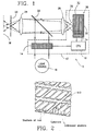
- the spatially light modulated confocal microscope of the background art indicated generally at 10 is schematically illustrated.
- the sequential spot scanning of conventional confocal microscopes is replaced by multiple pattern illumination (MPI), and the single channel detector, usually a photomultiplier tube, used with conventional sequential spot scanning is replaced by a two dimensional detector array masked by a conjugate aperture pattern which conforms with the multiple pattern illumination.
- Sequential complimentary patterns of illumination spots are imaged on an object.
- a confocal light modulation system 12 which forms the basic component of the spatially modulated confocal microscope 10, may be combined with the basic optics present in most conventional research microscopes to convert the research microscope to a confocal microscope.
- This confocal light modulation system includes a multiple pattern aperture array 14 which operates under the control of a central processor unit 16 to transform illuminated light from a light source 18 into sequential complimentary patterns of illumination spots which are imaged on a specimen 20 by means of a dichroic beam splitter 22 and a microscope objective lens 24.
- a conjugate array detector system 26 detects the light from the illuminated spots on the specimen which are transmitted via the beam splitter 22 and a lens or mirror 28.
- This array detector system includes a two-dimensional detector 30 which is masked by a conjugate aperture pattern unit 32 controlled by the central processor 16.
- the conjugate aperture pattern unit can be a separate unit or can constitute an addressed masking section of the detector 30.
- the conjugate aperture pattern unit masks the detector to define a conjugate aperture image corresponding to the pattern of the illuminated spots on the specimen onto the detector 30 in synchrony with the corresponding complimentary pattern formed by the multiple pattern aperture array 14.
- Both the conjugate aperture pattern unit and the multiple pattern aperture array and preferably high speed, pixelated arrays having a high pixel density which provide patterns of very small spots.
- the detector provides a video image output over lines 34 to the central processor unit which provides video image processing and display, or the detector could provide an output to a conventional video image processing and display system of known type.
- the multiple pattern aperture array 14 can take two forms; namely, interference patterns or patterned throughput from an aperture pattern. Interference patterns are complex and difficult to control, and interference pattern integrity will be compromised by the differences in refraction and birefringence across specimens of living tissue. Therefore, a multiple pattern aperture array 14 which provides direct aperture throughput is preferred for its simplicity, versatility and ease of implementation.
- Such a multiple pattern aperture array can be formed by an array of ferroelectric liquid crystal devices, by a digital mirror device, or by electrostatic microshutters of the type illustrated at 40 in Figure 2 . At rest, the microshutters block light from the light source 18, but when selected shutters are gated from the central processor 16, they open as illustrated at E in Figure 2 and pass light through to the specimen 20.
- Confocal imaging is possible by using two separate throughput aperture arrays operated in synchrony for the multiple pattern aperture array 14 and the conjugate aperture pattern unit 32.
- This requires extremely careful optical alignment and timing to implement.
- a simpler alternative is to employ an optical configuration that avoids use of two synchronously timed aperture arrays. This could be achieved by passing the image from the specimen back to the detector through the same aperture array used to form the multiple pattern aperture array 14, thus using this single array in place of the conjugate aperture pattern unit 32.
- the multiple pattern aperture array 14 would be positioned between the beam splitter 22 and the lens 24 in Figure 1 .
- this alternative requires precise optical alignment and would not provide a unit which could be easily attached to most conventional research microscopes.
- the conjugate aperture pattern unit 32 and detector 30 may be advantageously formed electronically by a CID camera or a charge-coupled device detector array (CCD) which uses computer aided image processing to enable the detector to disregard light returns from detector pixels which are not activated.
- a charge-coupled detector has the ability to acquire an entire image at once rather than by raster scanning.
- a complete bit map must be constructed of where active pixels are located on the CCD after calibration for each aperture pattern to be provided by the multiple pattern aperture array 14 under the control of the central processing unit 16. Calibration simply requires training the processing unit 16 which controls the CCD to disregard pixels which should not be read by placement of a mirror in the objective focal plane of the microscope so that each illumination pattern from the multiple pattern aperture array can be imaged directly on the CCD and stored by the central processing unit.
- Additional electronic and computer aided filtering after calibration may be required to clarify aperture boundaries and improve spatial resolution and sectioning capabilities, but once this is done, only light transmitted to the CCD for an associated pattern from the multiple pattern aperture array 14 is imaged, while light spillage to other areas of the CCD is ignored and effectively masked.
- This technique provides practical transmission confocal microscopy because the illumination subsystem does not use the same optical path as the imaging subsystem as is evident from Figure 1 .
- the detector pixel registers for the CCD device must be read rapidly in parallel for all lines. Therefore, special CCD pixel driver circuitry is required to optimize the detector for high speed applications.
- the need for the special driver circuitry required with a CCD detector to read lines in parallel can be eliminated by forming the detector 30 from an active pixel sensor (APS) rather than from a CCD.
- the active pixel sensor operates in a manner similar to that of a random access memory with each pixel containing its own selection and readout transistors. These transistors are monolithically integrated in the pixel for readout selection and amplifying or buffering the pixel output signal.
- An APS pixel pattern selected by the central processor 16 receives the light pattern from the specimen 20 and a photogenerated charge is integrated in each active pixel under a photogate. The selected pixels can be addressed simultaneously to provide output signals to an image processing system or to the central processing unit 16 for image processing.
- the multiple pattern aperture array 14 and, for some applications, the conjugate aperture pattern unit 32 may preferably be formed by a digital micro-mirror device of a type developed by Texas Instruments Inc. of Dallas, Texas, which includes a monolithic electrostatic, mirror-coated shutter array.
- These pixelated, micro-mechanical spatial light modulators are formed monolithically upon a silicon chip and include minor squares of highly reflective material suspended above the surface of silicon addressing circuitry by support pillar torsion bars.
- the addressing circuitry under each mirror pixel is a memory cell accessed by the central processor unit 16 which drives two electrodes under each mirror with complimentary signals. When a high logical level is applied to one of the electrodes, the mirror pixel rotates in a given direction with a total deflection of about 20° between two mirror states. 10° on either side of the perpendicular to the silicon water.
- FIG. 4 illustrates the basic structure of one pixel for a digital mirror device array.
- a mirror coated shutter 42 is mounted in contact with a conducting support layer 44 by torsion hinges 46.
- a spacer layer 48 separates the support layer 44 from a silicon chip 50.
- Each pixel of the digital mirror device array includes an address electrode 52 and a control or landing electrode 54 which, when activated, deflects the mirror coated shutter 42 around the torsion hinges 46.
- the mirror coated shutter 42 forms part of a multiple pattern aperture array mounted in the optical path of the illumination subsection 56 for a microscope, it may be positioned in a first position as shown in Figure 4 to direct a pixel of light along an optical path 58 to a specimen under observation.
- the mirror coated shutter 42 is deflected from the position of Figure 4 , the pixel of light is angled away from the specimen along an optical path 60.
- Software for the central processor unit 16 will enable a preprogrammed selection of any possible two dimensional pixel pattern within predetermined limits for confocal imaging. This technology provides the user with the flexibility to choose the pattern which offers the best combination of temporal and spacial resolution for a given application. The ability to custom make patterns can be geared for the correction of field distortion.
- the individual complementary images formed from each pixel pattern received by the detector 30 will be stored in the central processor unit 16 and subsequently overlaid to form one complete image frame for real-time imaging.
- the control software for the central processor 16 will be programmed to select stored aperture patterns designated by the user and, for some applications, to automatically select stored aperture patterns in response to sensed conditions such as the optical characteristics of a specimen.
- the processor software may also cause the processor to make a specimen-dependent background correction for each image frame. This is accomplished by sensing with the detector 30 a background image which may result with all illumination pixels of the multiple pattern aperture array 14 closed to block light from the light source 18, and then correcting in the processor the subsequent individual complimentary images formed from each pixel pattern by subtracting therefrom the effect created by the background image.
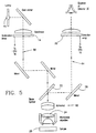
- Figure 5 illustrates one manner in which the confocal modulation system 12 may be incorporated into the structure of a conventional research microscope 62.
- the multiple pattern aperture array 14 is inserted into the optical path of the illumination subsystem 56 for the microscope while the conjugate aperture pattern unit 32 is inserted into the optical path of the microscope image subsection 64.
- the remaining optical components shown in Figure 5 are components of the research microscope 42.
- Specimens are usually non-luminous and must therefore be observed via light transmission, reflection, or fluorescence which requires the help of an auxiliary system consisting of an illumination source, condenser, and field aperture stops. Reflection or fluorescence observations usually employ epi-illumination where the microscope objective also functions as the condenser lens. Basic control of the illumination path and profile in any of these approaches usually employs one of two methods known as critical illumination and Köhler illumination.
- Critical illumination is achieved by placing the light source behind the field stop and imaging the source onto the object plane of the microscope objective.
- Köhler illumination an auxiliary lens, located behind the field stop, forms an image of the source in the back focal plane of the condenser.
- the object plane of the microscope objective is illuminated with superimposed collimated beams corresponding to each source point that tend to average out spatial irregularities in source brightness. For this reason.
- Köhler illumination is usually preferred over critical illumination. Nevertheless, Köhler illumination only approximates illumination uniformity and is not optimal for many applications.
- both reflective and transmissive confocal light modulated optical imaging systems have been developed wherein the conjugated illumination aperture and the detection aperture can be configured by double passing through a single digital micro-mirror device.
- Figure 6 illustrates a confocal light modulated optical imaging system indicated generally at 66 which uses all reflective components to perform 1:1 imaging. This system has no chromatic aberration and less spherical aberration.
- the system 66 includes a light source module 68 containing a light source 70 and any cooling fans required (not shown).
- the light source module is isolated from the remainder of the light modulated optical imaging system 66 and is connected thereto by a single mode optical fiber or optical fiber coupling bundles 72 which transmit light from the light source module while isolating the system from mechanical vibrations which may be present in the light source module.
- a coherent light source 70 a single mode optical fiber will be used for the coupling 72, while for an incoherent white light source, an optical fiber bundle will be used.
- Light from the coupling 72 is directed onto a parabolic mirror 74 and is reflected to a beam splitter 76. From the beam splitter, light is reflected to a first spherical mirror 78 and then to a second spherical mirror 80 which reflects it back to the first spherical mirror. The light is then reflected to mirrors 82 and 84 which direct light onto a computer controlled digital micro-mirror device 86 of the type previously described. Mirrors 82 and 84 are not always required for directing light to the digital mirror device 86. Without mirrors 82 and 84 light can also be directed to the digital mirror device 86 by rotating the angle of the optical system formed by the spherical mirrors 78 and 80.
- the device 86 can be an array of 864 x 756 mirrors that can be individually tilted ⁇ 10° dependent on the state of an associated binary memory cell. In one angle state a mirror will direct light down a light path 88 while in the second angle state the mirror will direct light to a parabolic mirror 90.
- the mirror 90 is provided to receive the deflected light and direct it into an optical cable or cable bundle 92 that returns this light to the coupling 72. This recycling of the unused difracted light both raises the light efficiency of the system while reducing heat dissipation in the area of the device 86 so that no cooling fan is required.
- the light pattern from the digital micro-mirror device 86 is directed along the light path 88 to a third spherical mirror 92 and is reflected thereby to a fourth spherical mirror 94.
- the pattern is then reflected from the spherical mirror 94 back to the spherical mirror 92 which reflects the pattern onto an image plane 96.
- the image plane 96 represents the image plane of a microscope objective which relays light to a specimen under observation.
- the image from the specimen is directed back to the image plane 96 and passes back along the same path followed by light from the light module 68. It is reflected back by the micro-mirror device 86 and when it reaches the beam splitter 76, it is directed onto the image plane 98 of a detector such as the detector 30.
- a detector such as the detector 30.
- Figure 7 illustrates a confocal light modulated optical imaging system 100 with a transmissive imaging means where components having a similar structure and operation to those shown in Figure 6 will be identified with like reference numerals.
- a combination of lenses and mirrors illuminate the digital micro-mirror device to generate the confocal scanning image.
- Light from the light module 68 and difracted light from the optical cable 92 is passed by the optical coupling 72 and the beam splitter 76 to a first lens 102 which transfers the light on a mirror 104.
- the mirror 104 then reflects the light onto the digital micro-mirror device 86, and the deflected light from the micro-mirror device is reflected by a mirror 106 through a lens 108 into the optical cable 92.
- the light pattern from the micro-mirror device is transmitted along the light path 88 and is transferred by a lens 110 on a mirror 112.
- the mirror 112 reflects the light pattern to a mirror 1 14 which in turn reflects the light pattern to a mirror 116.
- Mirror 116 reflects the light pattern onto a microscope image plane 118, which in the case of a transmissive confocal light modulated imaging system, is the image plane of the microscope illumination condenser on the side of the specimen which is opposite to the microscope objective.
- the light pattern from the specimen passes from the image plane 118 back over the same optical path taken by the light from the light module to the beam splitter 76.
- the beam splitter directs this light to a mirror 120 which then reflects the light pattern onto the image plane of a detector 122.
- any interaction between light and matter which alters a property of the incident light can be used to generate an optical image.
- wavelength, circular dichroism, and polarization are all properties of light that can be varied for image formation.
- Switching between left and right circularly polarized or linearly polarized light can be used to generate polarization difference images.
- the use of two fluorescent indicators, each operating in the single excitation mode, can be achieved by switching between two excitation wavelengths.
- variable dwell times the user can optimize the collection of data derived from two sources having different time scales. For example, a slowly changing pH signal could be monitored in the presence of a rapidly changing calcium signal using SNARF and Indo-1 in hypoxic brain slices.
- a spatially localized illumination system which is not part of the invention has been developed for operation in a dual wavelength mode.
- fluorescence ratio imaging will be implemented with acquisition rates independent of the illumination switching time between two system light sources.
- the system provides for controlled photolysis and pattern generation, rapid switching between two light sources and controlled field illumination.
- the system further offers the ability to maximize the signal to noise properties of ratio imaging by providing variable dwell time for the bound and free indicator compound. With this device, the total number of photons needed for a given signal to noise figure of merit can be achieved with both images used to form the ratio by compensation for differing fluorescence efficiencies with variable excitation exposure times.
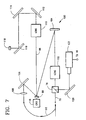
- MIMS 124 is designed to operate in a critical illumination mode and in an alternating dual source illumination mode.
- MIMS will provide computer-controlled and spatially localized illumination of an object plane over pixels approaching the diffraction limit.
- control paradigms for spatial photolysis of "caged" compounds, pattern generation for fluorescence recovery after photobleaching and photoactivation of fluorescence can be provided.
- MIMS provides submillisecond switching between two light sources.
- MIMS is a multipurpose illumination attachment that can be used in either the epi-illumination or condenser port of an optical microscope such as that shown in Figure 5 . It is also intended to be used as a light source for the confocal modulation systems shown in Figures 1 , 4 , 6 and 7 .
- the microscope illumination modulation system 124 includes first and second light sources 126 and 128 which provide light beams that are transferred respectively by lenses 130 and 132 and mirrors 134 and 136 onto a digital micro-mirror device 140 which is controlled by a processor 138 or other sequencing control unit.
- Figure 9 illustrates the basic optical diagram for one digital micro-mirror pixel 142.
- sequence A the mirror pixel 142 is inclined ten degrees to the right to direct a light beam from the light source 126 down an optical path 144 while diverting the light beam from the light source 128 away from the optical path.
- This diverted beam can be picked up by a light trap 146.
- a light trap 146 such as the parabolic mirror 90, which feeds light through a fiber optic cable back to the source.
- the mirror pixel 112 is inclined ten degrees to the left to direct a light beam from the light source 128 down the optical path 144 while diverting the light beam from the light source 126 away from the optical path.
- the lens and mirror combinations 130 and 134 and 132 and 136 are positioned and designed to direct the light beams from the light sources 126 and 128 at angles to the digital micro-mirror device 140 which enable the selected mirror pixels of the digital micro-mirror device to operate in the manner illustrated in Figure 9 .
- the digital micro-mirror device has an array of 864 x 756 mirror pixels that can be tilted plus or minus ten degrees dependent upon the zero or one state of an associated binary memory cell. The mirrors can switch between these two angle states in only 30 microseconds.
- the microscope illumination modulation system 124 When the microscope illumination modulation system 124 is used in the critical illumination mode, an image of the digital micro-mirror device will be generated in the object plane of the microscope. Using a standard computer interface, (mouse, touchpad, pen, etc.) the operator will be able to outline an area or areas on the computer display for subsequent illumination by one or more illumination sources coupled to the MIMS 124. When the external light sources are triggered, only the defined area will be illuminated. Neurotransmitters could be released from caged precursors in dendritic regions. Specific chromosomes could be targeted for ablation in chromosome surgery.
- the digital micro-mirror device In the alternating dual-source illumination mode of the MIMS 124, the digital micro-mirror device will be used to switch between the two external light sources.
- the operator can use either the processor 138 to control the switching rate and duty cycle or some other external synchronization source. This control will allow optimal illumination of dual-excitation single-emission fluorescent compounds such as the calcium indicator Fura-2.
- Köhler illumination will be used to illuminate the surface of the digital micro-mirror device.
- Köhler illumination is a method of adjusting the illumination system of a microscope which offers several advantages including maximizing contrast, and lateral and axial resolution. Maximum performance is achieved by illuminating the specimens with a converging set of plane wave fronts, each arising from an image of the source in the condenser aperture and conjugate with the back focal plane of the objective. Optimum performance is only achieved when the condenser aperture is uniformly illuminated. This is difficult to achieve with concentrated arc-lamps which are highly nonuniform. Often, luminous density is sacrificed by over-filling the aperture in order to approximate uniform illumination.
- MIMS 124 has the ability to control the illumination of the condenser aperture using the digital micro-mirror device to create a time-varying mask. This feature will enhance the use of the microscope in any of the modes of microscopy which rely on uniform illumination to generate image contrast. These modes include phase contrast, interference contrast, differential interference contrast, modulation contrast, darkfield, absorption, reflection, polarization and fluorescence.
- the mirrors 134 and 136 would direct light from a respective light source on an area of the micro-mirror device 140 which does not receive light from the remaining light source and the pixels in each area would be separately controlled by the processor 138.
- the light sources 126 and 128 would provide light of different colors. Other differing light characteristics could be separately provided by these two light sources and simultaneously projected.
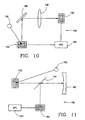
- FIG 10 illustrates a spatially light modulated optical lens testing instrument and method for real time lens aberration testing.
- the lens testing instrument indicated generally at 148 includes a light source 150 which projects light on a digital micro-mirror device 152 that is controlled by a processor 154.
- An optical system indicated for illustrative purposes as a mirror 156, directs light from the digital micro-mirror device 152 along an optical path through a lens 158 under test.
- Each pixel mirror of the digital micro-mirror device can constitute a separate beam source under the control of the processor 154, although for illustrative purposes, only two of such beams are shown in Figure 10 .
- Each beam passes through the test lens and contacts an optical detector 160 at a definite location.
- each pixel beam on the detector is indicative of the condition of the test lens 158, for with a properly configured lens, each beam will contact the detector at a defined contact point programmed in the processor 154. Deviation of the beam from this defined contact point indicated aberration in the lens in the area through which the beam passes, and detector position data indicative of this deviation is fed to the processor 154 where it is compared with the stored position data to obtain deviation data values.
- These deviation data values can be used in a printout or display to indicate where and to what degree lens correction is required or can be directed as control data for a lens grinder or other lens formation device to directly control correction of the test lens 158.
- the-lens testing instrument can include optical components in addition to those shown diagrammatically in Figure 10 .
- a reflective lens test system can employ the complete confocal light modulated optical system 66 of Figure 6 with the exception that the lens 158 under test would be placed in the position of the image plane 96 and a mirror 162, shown in broken lines in Figure 6 would be placed behind the lens 158 to reflect the pixel beams back to the spherical mirror 92 and back along the light path to the image plane 98 of the detector 160.
- optical components other than lenses can be tested using a testing instrument similar to that of Figure 10 .
- the testing instrument 148 is used to test a mirror 162 rather than a lens, and employs a beam splitter 164 to direct light reflected from the test mirror to the optical detector 160.
- the optical component test system 148 uses each pixel in a spatial light modulator (e.g., micro-mirror device 152) to generate a real-time ray tracing.
- the ray tracings pass through a test lens or are reflected by a test mirror and finally reach a two-dimensional detector 160 (e.g., CID or CCD) which is conjugated to the spatial light modulator plane in object-image relation.
- a spatial light modulator e.g., micro-mirror device 152
- the ray tracings pass through a test lens or are reflected by a test mirror and finally reach a two-dimensional detector 160 (e.g., CID or CCD) which is conjugated to the spatial light
- the position and the distribution of the ray tracings on the detector plane indicate the aberration situation of the test optical component.
- the signal processing means implemented in central processor unit (CPU) 154 retrieves the structural information of the test optical component after it collects the position and the distribution of the ray tracings on the detector plane.
- a way to improve the SNR of a confocal image can comprise the following steps.
- In the first step use a large illumination aperture and a large detection aperture to get a confocal image which has a high SNR and low axial resolution.
- In the second step use another different large illumination aperture and a large detection aperture to get another confocal image which has a high SNR and low axial resolution.
- In the third step use the difference of said confocal images to get the final confocal image which has both high SNR and high axial resolution
- imaging modes e.g., confocal scanning imaging mode, wide-field fluorescence imaging mode, bright field imaging mode, dark field imaging mode, contrast (phase contrast, modulation contrast, interference contrast, and polarization contrast) imaging modes, will get different information.
- contrast phase contrast, modulation contrast, interference contrast, and polarization contrast
- the system comprises the following elements and relationships; namely, a group of discrete, analog or digital detection elements sampling the detection plane, an object plane, which samples a slice of sample, substantially conjugating with both said illumination plane and said detection plane in object-image relationships, a set of complimentary confocal patterns formed by said illumination elements and said detection elements generating a confocal imaging mode.
- a group of discrete, analog or digital detection elements sampling the detection plane
- an object plane which samples a slice of sample, substantially conjugating with both said illumination plane and said detection plane in object-image relationships
- a set of complimentary confocal patterns formed by said illumination elements and said detection elements generating a confocal imaging mode.
- the spatially light modulated confocal optical instruments and method provide conjugate aperture image formation to counter the deficiencies of known devices such as scanning confocal microscopes.
- the confocal light modulation system may be used to convert a conventional research microscope into a confocal microscope having enhanced capabilities. Since the unit has no moving parts and is vibration free, it is suitable for sensitive micro-manipulation and intracellular recording techniques common in neurophysiological studies.
- the high speed imaging capability of the unit renders it suitable for use to follow dendritic and synaptic changes in neurons on the millisecond scale or to measure kinetics in response to drugs or fluorescent indicators for intracellular pH, calcium, sodium, etc.
- the spatially light modulated confocal optical instrument is particularly well adapted for use in the high speed inspection of silicon wafers for quality control purposes in integrated circuit production, and for testing high quality lenses.
Landscapes
- Physics & Mathematics (AREA)
- General Physics & Mathematics (AREA)
- Optics & Photonics (AREA)
- Chemical & Material Sciences (AREA)
- Analytical Chemistry (AREA)
- Geometry (AREA)
- Microscoopes, Condenser (AREA)
Claims (4)
- Konfokales optisches Abbildungssystem (66; 100) zum Abbilden einer Probe, aufweisend:eine Lichtquelle (70), um Licht der Probe zuzuführen,optisches Kopplermittel (72), um Licht von der Lichtquelle entlang einem Beleuchtungspfad auf die Probe zu richten,Musterarraymittel (86), die in dem Beleuchtungspfad zwischen der Lichtquelle und der Probe angeordnet sind, wobei das Musterarraymittel betriebsmäßig Licht von der Lichtquelle in eine Vielzahl von simultan gebildeten Beleuchtungspunkten, die zu einem Muster angeordnet sind, umwandelt und Licht außerhalb des Musters ablenkt,optisches Abbildungsmittel (92, 94; 110) zum simultanen Abbilden des Musters aus Beleuchtungspunkten auf die Probe,Lichtempfangsmittel (90, 108), das derart befestigt ist, dass es durch das Musterarraymittel abgelenktes Licht empfängt, und Lichtübertragungsmittel (92), um Licht von dem Lichtempfangsmittel zu dem optischen Kopplermittel zu übertragen, um so ebenfalls Licht von dem Lichtübertragungsmittel entlang dem Beleuchtungspfad auf die Probe zu richten.
- Konfokales Abbildungssystem nach Anspruch 1, wobei das Lichtübertragungsmittel eine flexible Lichtleitfaser umfasst zum Leiten von Licht von dem Lichtempfangsmittel zu dem optischen Kopplermittel.
- Konfokales optisches Abbildungssystem nach Anspruch 2, wobei das Musterarraymittel in Antwort auf Steuersignale betriebsfähig ist, um sequentielle Muster aus Beleuchtungspunkten vorzusehen, und wobei ein Steuermittel (16) vorgesehen ist, das mit dem Musterarraymittel verbunden ist, und wobei das Steuermittel betriebsmäßig Steuersignale dem Musterarraymittel liefert, um zu bewirken, dass das Musterarraymittel sequentielle komplimentäre Muster aus Beleuchtungspunkten vorsieht.
- Konfokales optisches Abbildungssystem nach Anspruch 2, wobei das Musterarraymittel eine digitale Spiegelvorrichtung umfasst, die ein spiegelbeschichtetes Verschlussarray besitzt.
Applications Claiming Priority (3)
| Application Number | Priority Date | Filing Date | Title |
|---|---|---|---|
| US770423 | 1985-08-29 | ||
| US08/770,423 US5923466A (en) | 1993-10-20 | 1996-12-20 | Light modulated confocal optical instruments and method |
| PCT/US1997/022969 WO1998028655A2 (en) | 1996-12-20 | 1997-12-19 | Light modulated confocal optical instruments and method |
Publications (3)
| Publication Number | Publication Date |
|---|---|
| EP0948754A2 EP0948754A2 (de) | 1999-10-13 |
| EP0948754A4 EP0948754A4 (de) | 2000-08-09 |
| EP0948754B1 true EP0948754B1 (de) | 2014-06-04 |
Family
ID=25088485
Family Applications (1)
| Application Number | Title | Priority Date | Filing Date |
|---|---|---|---|
| EP97952425.3A Expired - Lifetime EP0948754B1 (de) | 1996-12-20 | 1997-12-19 | Lichtmoduliertes konfokales optisches instrument |
Country Status (4)
| Country | Link |
|---|---|
| US (1) | US5923466A (de) |
| EP (1) | EP0948754B1 (de) |
| AU (1) | AU5603198A (de) |
| WO (1) | WO1998028655A2 (de) |
Cited By (3)
| Publication number | Priority date | Publication date | Assignee | Title |
|---|---|---|---|---|
| WO2018205357A1 (zh) * | 2017-05-12 | 2018-11-15 | 中国科学院苏州生物医学工程技术研究所 | 结构光照明显微成像系统 |
| CN110275288A (zh) * | 2019-06-21 | 2019-09-24 | 无锡迅杰光远科技有限公司 | 一种多向mems扫描装置 |
| DE102022117536A1 (de) | 2022-07-13 | 2024-01-18 | Precitec Optronik Gmbh | Vorrichtung zur chromatisch konfokalen Messung von Abständen |
Families Citing this family (72)
| Publication number | Priority date | Publication date | Assignee | Title |
|---|---|---|---|---|
| US6483641B1 (en) * | 1997-10-29 | 2002-11-19 | Digital Optical Imaging Corporation | Apparatus and methods relating to spatially light modulated microscopy |
| US6388809B1 (en) | 1997-10-29 | 2002-05-14 | Digital Optical Imaging Corporation | Methods and apparatus for improved depth resolution use of out-of-focus information in microscopy |
| DE19824460A1 (de) | 1998-05-30 | 1999-12-02 | Zeiss Carl Jena Gmbh | Anordnung und Verfahren zur mikroskopischen Erzeugung von Objektbildern |
| DE19853407C2 (de) * | 1998-11-19 | 2003-09-11 | Leica Microsystems | Verfahren zur Einstellung der Systemparameter eines konfokalen Laserscanmikroskops |
| US6426835B1 (en) | 1999-03-23 | 2002-07-30 | Olympus Optical Co., Ltd. | Confocal microscope |
| AU4500100A (en) * | 1999-04-30 | 2000-11-17 | Digital Optical Imaging Corporation | Methods and apparatus for improved depth resolution using out-of-focus information in microscopy |
| US6268908B1 (en) * | 1999-08-30 | 2001-07-31 | International Business Machines Corporation | Micro adjustable illumination aperture |
| US20030139667A1 (en) * | 2000-04-13 | 2003-07-24 | Hewko Mark D. | Tissue viability/health monitor utilizing near infrared spectroscopy |
| US6747795B2 (en) * | 2000-06-30 | 2004-06-08 | The General Hospital Corporation | Fiber-coupled multiplexed confocal microscope |
| US6545758B1 (en) * | 2000-08-17 | 2003-04-08 | Perry Sandstrom | Microarray detector and synthesizer |
| WO2002014811A1 (de) * | 2000-08-17 | 2002-02-21 | Mg Microscope Gmbh | Lichterfassungseinheit und verfahren zum erfassen von lumineszenzlicht sowie konfokales mikroskop für die lumineszenzmikroskopie |
| US6567163B1 (en) | 2000-08-17 | 2003-05-20 | Able Signal Company Llc | Microarray detector and synthesizer |
| DE10116723C1 (de) * | 2001-04-04 | 2002-10-31 | Bosch Gmbh Robert | Vorrichtung zur Ablenkung von optischen Strahlen |
| WO2003025656A1 (en) * | 2001-09-03 | 2003-03-27 | Kabushiki Kaisha Hayashi Soken | Digital control scanning method and apparatus |
| JP5048899B2 (ja) * | 2001-09-28 | 2012-10-17 | オリンパス株式会社 | 顕微鏡 |
| US6658315B2 (en) * | 2001-10-31 | 2003-12-02 | Ball Semiconductor, Inc. | Non-synchronous control of pulsed light |
| US6885492B2 (en) * | 2001-11-08 | 2005-04-26 | Imaginative Optics, Inc. | Spatial light modulator apparatus |
| DE10155142C2 (de) * | 2001-11-12 | 2003-09-04 | Friz Biochem Gmbh | Dunkelfeld-Abbildungsvorrichtung zur ortsaufgelösten Dunkelfeldabbildung einer flächigen Probe |
| US7756305B2 (en) * | 2002-01-23 | 2010-07-13 | The Regents Of The University Of California | Fast 3D cytometry for information in tissue engineering |
| US6987259B2 (en) * | 2002-05-30 | 2006-01-17 | Dmetrix, Inc. | Imaging system with an integrated source and detector array |
| US7049570B2 (en) * | 2002-09-16 | 2006-05-23 | Avago Technologies, Ltd. | Optical chip coupling system utilizing micromachine adjustable optical elements and a feedback circuit providing the micromachine with a feedback signal correlated to an optical signal parameter |
| US20040120577A1 (en) * | 2002-10-06 | 2004-06-24 | Igor Touzov | Digital video based array detector for parallel process control and radiation driver for micro-scale devices |
| DE10258945A1 (de) * | 2002-12-17 | 2004-07-01 | Olympus Biosystems Gmbh | Fluoreszenzbasierte optische Objektuntersuchungseinrichtung, insbesondere für die TIRF-Mikroskopie |
| US7141801B2 (en) * | 2002-12-26 | 2006-11-28 | Applied Precision, Llc | System and method of illuminating living cells for imaging |
| DE602004024464D1 (de) * | 2003-07-04 | 2010-01-14 | Vincent Lauer | Bildgebungsvorrichtung für konfokale Mikroskopie mit Bildsubstraktion |
| DE10347326B4 (de) | 2003-10-11 | 2022-08-04 | Leica Microsystems Cms Gmbh | Anordnung mit einem Mikroskop und einem Modul |
| US20050157299A1 (en) * | 2004-01-15 | 2005-07-21 | Heffelfinger David M. | Optical analysis systems |
| US20050269523A1 (en) * | 2004-03-24 | 2005-12-08 | Macaulay Calum E | Light modulated microarray reader and methods relating thereto |
| US20050283498A1 (en) * | 2004-06-22 | 2005-12-22 | Taiwan Semiconductor Manufacturing Company, Ltd. | System and method to build, retrieve and track information in a knowledge database for trouble shooting purposes |
| US20060066842A1 (en) * | 2004-09-30 | 2006-03-30 | Saunders Winston A | Wafer inspection with a customized reflective optical channel component |
| US20060275672A1 (en) * | 2005-06-06 | 2006-12-07 | Wintek Corporation | Photomask with controllable patterns |
| US7460248B2 (en) * | 2006-05-15 | 2008-12-02 | Carestream Health, Inc. | Tissue imaging system |
| DE102006027836B4 (de) * | 2006-06-16 | 2020-02-20 | Carl Zeiss Microscopy Gmbh | Mikroskop mit Autofokuseinrichtung |
| DE102006045692A1 (de) * | 2006-09-27 | 2008-04-03 | Osram Opto Semiconductors Gmbh | Optisches Projektionsgerät |
| US8300207B2 (en) | 2007-05-17 | 2012-10-30 | Nikon Corporation | Exposure apparatus, immersion system, exposing method, and device fabricating method |
| DE102008034137A1 (de) | 2007-09-28 | 2009-04-02 | Carl Zeiss Microlmaging Gmbh | Mikroskop und Verfahren zum Betreiben eines Mikroskops |
| US20090112482A1 (en) * | 2007-10-26 | 2009-04-30 | Sandstrom Perry L | Microarray detector and synthesizer |
| WO2009066672A1 (ja) * | 2007-11-19 | 2009-05-28 | Nikon Corporation | 干渉計 |
| US8077294B1 (en) | 2008-01-17 | 2011-12-13 | Ball Aerospace & Technologies Corp. | Optical autocovariance lidar |
| US8119971B2 (en) | 2008-01-17 | 2012-02-21 | Ball Corporation | Pulse data recorder in which a value held by a bit of a memory is determined by a state of a switch |
| US8725477B2 (en) * | 2008-04-10 | 2014-05-13 | Schlumberger Technology Corporation | Method to generate numerical pseudocores using borehole images, digital rock samples, and multi-point statistics |
| US9581723B2 (en) | 2008-04-10 | 2017-02-28 | Schlumberger Technology Corporation | Method for characterizing a geological formation traversed by a borehole |
| US7961301B2 (en) | 2008-05-09 | 2011-06-14 | Ball Aerospace & Technologies Corp. | Flash LADAR system |
| US9041915B2 (en) | 2008-05-09 | 2015-05-26 | Ball Aerospace & Technologies Corp. | Systems and methods of scene and action capture using imaging system incorporating 3D LIDAR |
| US7929215B1 (en) | 2009-02-20 | 2011-04-19 | Ball Aerospace & Technologies Corp. | Field widening lens |
| WO2010099328A2 (en) | 2009-02-25 | 2010-09-02 | The University Of Memphis Research Foundation | Spatially-selective reflector structures, reflector disks, and systems and methods for use thereof |
| US20110004447A1 (en) * | 2009-07-01 | 2011-01-06 | Schlumberger Technology Corporation | Method to build 3D digital models of porous media using transmitted laser scanning confocal mircoscopy and multi-point statistics |
| US8311788B2 (en) | 2009-07-01 | 2012-11-13 | Schlumberger Technology Corporation | Method to quantify discrete pore shapes, volumes, and surface areas using confocal profilometry |
| JP5591007B2 (ja) * | 2009-11-20 | 2014-09-17 | オリンパス株式会社 | 顕微鏡装置 |
| US8306273B1 (en) | 2009-12-28 | 2012-11-06 | Ball Aerospace & Technologies Corp. | Method and apparatus for LIDAR target identification and pose estimation |
| JP5665369B2 (ja) * | 2010-05-27 | 2015-02-04 | キヤノン株式会社 | 撮像装置 |
| US8736818B2 (en) | 2010-08-16 | 2014-05-27 | Ball Aerospace & Technologies Corp. | Electronically steered flash LIDAR |
| GB201019181D0 (en) | 2010-11-12 | 2010-12-29 | Univ Leicester | Improved optical arrangement |
| US8780345B2 (en) | 2011-04-22 | 2014-07-15 | The University Of Memphis Research Foundation | Spatially-selective disks, submillimeter imaging devices, methods of submillimeter imaging, profiling scanners, spectrometry devices, and methods of spectrometry |
| US8237835B1 (en) | 2011-05-19 | 2012-08-07 | Aeon Imaging, LLC | Confocal imaging device using spatially modulated illumination with electronic rolling shutter detection |
| JP5864177B2 (ja) * | 2011-09-15 | 2016-02-17 | 船井電機株式会社 | プロジェクタおよびプロジェクタシステム |
| US9137433B2 (en) * | 2011-09-19 | 2015-09-15 | Michael Mojaver | Super resolution binary imaging and tracking system |
| US20130070091A1 (en) | 2011-09-19 | 2013-03-21 | Michael Mojaver | Super resolution imaging and tracking system |
| US10924668B2 (en) | 2011-09-19 | 2021-02-16 | Epilog Imaging Systems | Method and apparatus for obtaining enhanced resolution images |
| JPWO2013089258A1 (ja) * | 2011-12-15 | 2015-04-27 | 株式会社ニコン | 顕微鏡及び刺激装置 |
| WO2013095481A1 (en) * | 2011-12-22 | 2013-06-27 | Draeger Medical System, Inc. | Dynamic light filtering device and method for enhanced patient parameter monitoring |
| US8744126B1 (en) | 2012-03-07 | 2014-06-03 | Ball Aerospace & Technologies Corp. | Morphology based hazard detection |
| WO2014155262A1 (en) * | 2013-03-25 | 2014-10-02 | Gandolfi Daniela | An image forming method of a fluorescent sample |
| US9347852B1 (en) | 2013-05-08 | 2016-05-24 | Thomas DiMatteo | Microscope illumination diagnostic cube |
| JP6513980B2 (ja) * | 2015-03-16 | 2019-05-15 | 株式会社東芝 | 撮像装置及び撮像方法 |
| DE102015111282A1 (de) * | 2015-07-13 | 2017-01-19 | Stiftung Caesar Center Of Advanced European Studies And Research | Verfahren zum Beobachten eines chemischen und/oder biologischen Vorgangs |
| EP3130842B1 (de) * | 2015-07-15 | 2019-09-25 | CoeLux S.r.l. | Lichtkuppelbeleuchtungssystem |
| WO2017058901A1 (en) | 2015-09-28 | 2017-04-06 | Ball Aerospace & Technologies Corp. | Differential absorption lidar |
| US10921245B2 (en) | 2018-06-08 | 2021-02-16 | Ball Aerospace & Technologies Corp. | Method and systems for remote emission detection and rate determination |
| CN112859315A (zh) * | 2021-01-11 | 2021-05-28 | 北京大学 | 一种多色双模式结构光照明显微成像系统及其成像方法 |
| US20240230316A1 (en) * | 2021-06-22 | 2024-07-11 | The General Hospital Corporation | Apparatus and methods to enhance signal to noise ratio imaging performance in optical coherence tomography |
| EP4550021B1 (de) | 2023-11-06 | 2025-12-31 | Valstybinis Moksliniu Tyrimu Institutas Fiziniu Ir Technologijos Mokslu Centras | Konfokale mikroskopie mit schneller und programmierbarer reflexion mit digitaler mikrospiegelvorrichtung |
Family Cites Families (32)
| Publication number | Priority date | Publication date | Assignee | Title |
|---|---|---|---|---|
| US3013467A (en) * | 1957-11-07 | 1961-12-19 | Minsky Marvin | Microscopy apparatus |
| US3877788A (en) * | 1973-03-30 | 1975-04-15 | Itek Corp | Method and apparatus for testing lenses |
| US3926500A (en) * | 1974-12-02 | 1975-12-16 | Ibm | Method of increasing the depth of focus and or the resolution of light microscopes by illuminating and imaging through a diaphragm with pinhole apertures |
| GB1595422A (en) * | 1977-04-28 | 1981-08-12 | Nat Res Dev | Scaning microscopes |
| US4561731A (en) * | 1980-03-10 | 1985-12-31 | Kley Victor B | Electronic illumination control |
| US4634880A (en) * | 1982-04-19 | 1987-01-06 | Siscan Systems, Inc. | Confocal optical imaging system with improved signal-to-noise ratio |
| US4601537A (en) * | 1984-01-06 | 1986-07-22 | Ohio State University Research Foundation | Apparatus and methods for forming images and for optical demultiplexing |
| US4699498A (en) * | 1985-09-06 | 1987-10-13 | Nec Corporation | Image projector with liquid crystal light shutter |
| NL8700612A (nl) * | 1987-03-13 | 1988-10-03 | Tno | Confocale laserscanning microscoop. |
| US4806004A (en) * | 1987-07-10 | 1989-02-21 | California Institute Of Technology | Scanning microscopy |
| US5099363A (en) * | 1987-09-24 | 1992-03-24 | Washington University | Method and apparatus for slow aperture scanning in a single aperture confocal scanning EPI-illumination microscope |
| US4802748A (en) * | 1987-12-14 | 1989-02-07 | Tracor Northern, Inc. | Confocal tandem scanning reflected light microscope |
| US5144477A (en) * | 1988-04-11 | 1992-09-01 | Medical Research Council | Method of operating a scanning confocal imaging system |
| US5032720A (en) * | 1988-04-21 | 1991-07-16 | White John G | Confocal imaging system |
| JPH0378720A (ja) * | 1989-08-22 | 1991-04-03 | Nikon Corp | 共焦点型レーザ走査顕微鏡 |
| US5065008A (en) * | 1989-10-18 | 1991-11-12 | Fuji Photo Film Co., Ltd. | Scanning microscope and scanning mechanism for the same |
| JP2561160B2 (ja) * | 1989-11-06 | 1996-12-04 | 富士写真フイルム株式会社 | 走査型顕微鏡 |
| US5067805A (en) * | 1990-02-27 | 1991-11-26 | Prometrix Corporation | Confocal scanning optical microscope |
| JP2613118B2 (ja) * | 1990-04-10 | 1997-05-21 | 富士写真フイルム株式会社 | 共焦点走査型顕微鏡 |
| US5035476A (en) * | 1990-06-15 | 1991-07-30 | Hamamatsu Photonics K.K. | Confocal laser scanning transmission microscope |
| GB9016632D0 (en) * | 1990-07-28 | 1990-09-12 | Medical Res Council | Confocal imaging system for microscopy |
| US5239178A (en) * | 1990-11-10 | 1993-08-24 | Carl Zeiss | Optical device with an illuminating grid and detector grid arranged confocally to an object |
| US5138459A (en) * | 1990-11-20 | 1992-08-11 | Personal Computer Cameras, Inc. | Electronic still video camera with direct personal computer (pc) compatible digital format output |
| JP3066157B2 (ja) * | 1990-12-31 | 2000-07-17 | テキサス インスツルメンツ インコーポレイテツド | タングステン光の照明の均一性のための装置と方法 |
| US5162941A (en) * | 1991-07-23 | 1992-11-10 | The Board Of Governors Of Wayne State University | Confocal microscope |
| US5187539A (en) * | 1991-09-23 | 1993-02-16 | Rockwell International Corporation | Mirror surface characteristic testing |
| US5260826A (en) * | 1992-01-21 | 1993-11-09 | Physical Optics Corporation | Nonscanning sectioning microscope |
| US5295017A (en) * | 1992-08-27 | 1994-03-15 | Bio-Rad Laboratories, Inc. | Sample masking using wavelength-selective material |
| US5386250A (en) * | 1993-08-09 | 1995-01-31 | Philips Electronics North America Corp. | Two-source illumination system |
| KR950704670A (ko) * | 1993-09-30 | 1995-11-20 | 가따다 데쯔야 | 공초점광학장치 |
| US5587832A (en) * | 1993-10-20 | 1996-12-24 | Biophysica Technologies, Inc. | Spatially light modulated confocal microscope and method |
| DE4416314C2 (de) * | 1994-05-09 | 1997-06-12 | Agfa Gevaert Ag | Verfahren und Vorrichtung zur Aufnahme einer Bildszene und Verwendung der Vorrichtung in einem Kopiergerät |
-
1996
- 1996-12-20 US US08/770,423 patent/US5923466A/en not_active Expired - Lifetime
-
1997
- 1997-12-19 AU AU56031/98A patent/AU5603198A/en not_active Abandoned
- 1997-12-19 EP EP97952425.3A patent/EP0948754B1/de not_active Expired - Lifetime
- 1997-12-19 WO PCT/US1997/022969 patent/WO1998028655A2/en not_active Ceased
Cited By (5)
| Publication number | Priority date | Publication date | Assignee | Title |
|---|---|---|---|---|
| WO2018205357A1 (zh) * | 2017-05-12 | 2018-11-15 | 中国科学院苏州生物医学工程技术研究所 | 结构光照明显微成像系统 |
| US11681135B2 (en) | 2017-05-12 | 2023-06-20 | Suzhou Institute Of Biomedical Engineering And Technology, Chinese Academy Of Sciences | Structured illumination microscopic imaging system |
| CN110275288A (zh) * | 2019-06-21 | 2019-09-24 | 无锡迅杰光远科技有限公司 | 一种多向mems扫描装置 |
| CN110275288B (zh) * | 2019-06-21 | 2021-06-22 | 无锡迅杰光远科技有限公司 | 一种多向mems扫描装置 |
| DE102022117536A1 (de) | 2022-07-13 | 2024-01-18 | Precitec Optronik Gmbh | Vorrichtung zur chromatisch konfokalen Messung von Abständen |
Also Published As
| Publication number | Publication date |
|---|---|
| EP0948754A2 (de) | 1999-10-13 |
| AU5603198A (en) | 1998-07-17 |
| WO1998028655A3 (en) | 1998-10-08 |
| US5923466A (en) | 1999-07-13 |
| EP0948754A4 (de) | 2000-08-09 |
| WO1998028655A2 (en) | 1998-07-02 |
Similar Documents
| Publication | Publication Date | Title |
|---|---|---|
| EP0948754B1 (de) | Lichtmoduliertes konfokales optisches instrument | |
| US5587832A (en) | Spatially light modulated confocal microscope and method | |
| US10527834B2 (en) | Functionally integrated laser scanning microscope | |
| Matsumoto | Cell biological applications of confocal microscopy | |
| EP1580586B1 (de) | Scannendes konfokales Mikroskop | |
| JP6996048B2 (ja) | 広視野高分解能顕微鏡 | |
| US7212338B2 (en) | Arrangement for illumination and/or detection in a microscope | |
| US20210231936A1 (en) | Single plane illumination microscope | |
| US8970950B2 (en) | Single plane illumination microscope | |
| US7706584B2 (en) | Random access high-speed confocal microscope | |
| US20090046360A1 (en) | Raster scanning light microscope with line pattern scanning and applications | |
| US20080285123A1 (en) | Raster scanning light microscope | |
| US20090218527A1 (en) | Confocal Microscopy with a Two-Dimensional Array of Light Emitting Diodes | |
| CN111095073B (zh) | 在激光扫描显微镜中扫描激发辐射和/或操纵辐射的光学组件以及激光扫描显微镜 | |
| WO2023221400A1 (zh) | 超分辨单物镜光片显微成像光学系统及其成像系统 | |
| US11314072B2 (en) | Microscope system with light sheet microscopy functional unit | |
| EP1265092B1 (de) | Vorrichtung und Verfahren für ROI-Abtastung mit hoher zeitlicher Auflösung | |
| US20060012874A1 (en) | Raster scanning light microscope with punctiform light source distribution and applications | |
| US20050146784A1 (en) | Confocal microscope having multiple independent excitation paths | |
| Kawamura et al. | Confocal laser microscope scanner and CCD camera |
Legal Events
| Date | Code | Title | Description |
|---|---|---|---|
| PUAI | Public reference made under article 153(3) epc to a published international application that has entered the european phase |
Free format text: ORIGINAL CODE: 0009012 |
|
| 17P | Request for examination filed |
Effective date: 19990715 |
|
| AK | Designated contracting states |
Kind code of ref document: A2 Designated state(s): AT BE CH DE DK ES FI FR GB GR IE IT LI LU MC NL PT SE |
|
| RIC1 | Information provided on ipc code assigned before grant |
Free format text: 7G 02F 1/00 A, 7G 02B 21/00 B |
|
| A4 | Supplementary search report drawn up and despatched |
Effective date: 20000623 |
|
| AK | Designated contracting states |
Kind code of ref document: A4 Designated state(s): AT BE CH DE DK ES FI FR GB GR IE IT LI LU MC NL PT SE |
|
| 17Q | First examination report despatched |
Effective date: 20040511 |
|
| RAP1 | Party data changed (applicant data changed or rights of an application transferred) |
Owner name: OLYMPUS CORPORATION |
|
| GRAP | Despatch of communication of intention to grant a patent |
Free format text: ORIGINAL CODE: EPIDOSNIGR1 |
|
| GRAP | Despatch of communication of intention to grant a patent |
Free format text: ORIGINAL CODE: EPIDOSNIGR1 |
|
| INTG | Intention to grant announced |
Effective date: 20131114 |
|
| GRAS | Grant fee paid |
Free format text: ORIGINAL CODE: EPIDOSNIGR3 |
|
| GRAA | (expected) grant |
Free format text: ORIGINAL CODE: 0009210 |
|
| AK | Designated contracting states |
Kind code of ref document: B1 Designated state(s): AT BE CH DE DK ES FI FR GB GR IE IT LI LU MC NL PT SE |
|
| REG | Reference to a national code |
Ref country code: GB Ref legal event code: FG4D |
|
| REG | Reference to a national code |
Ref country code: CH Ref legal event code: EP |
|
| REG | Reference to a national code |
Ref country code: AT Ref legal event code: REF Ref document number: 671387 Country of ref document: AT Kind code of ref document: T Effective date: 20140615 |
|
| REG | Reference to a national code |
Ref country code: IE Ref legal event code: FG4D |
|
| REG | Reference to a national code |
Ref country code: DE Ref legal event code: R096 Ref document number: 69740715 Country of ref document: DE Effective date: 20140717 |
|
| REG | Reference to a national code |
Ref country code: AT Ref legal event code: MK05 Ref document number: 671387 Country of ref document: AT Kind code of ref document: T Effective date: 20140604 |
|
| REG | Reference to a national code |
Ref country code: NL Ref legal event code: VDEP Effective date: 20140604 |
|
| PG25 | Lapsed in a contracting state [announced via postgrant information from national office to epo] |
Ref country code: GR Free format text: LAPSE BECAUSE OF FAILURE TO SUBMIT A TRANSLATION OF THE DESCRIPTION OR TO PAY THE FEE WITHIN THE PRESCRIBED TIME-LIMIT Effective date: 20140905 Ref country code: FI Free format text: LAPSE BECAUSE OF FAILURE TO SUBMIT A TRANSLATION OF THE DESCRIPTION OR TO PAY THE FEE WITHIN THE PRESCRIBED TIME-LIMIT Effective date: 20140604 |
|
| PG25 | Lapsed in a contracting state [announced via postgrant information from national office to epo] |
Ref country code: SE Free format text: LAPSE BECAUSE OF FAILURE TO SUBMIT A TRANSLATION OF THE DESCRIPTION OR TO PAY THE FEE WITHIN THE PRESCRIBED TIME-LIMIT Effective date: 20140604 Ref country code: AT Free format text: LAPSE BECAUSE OF FAILURE TO SUBMIT A TRANSLATION OF THE DESCRIPTION OR TO PAY THE FEE WITHIN THE PRESCRIBED TIME-LIMIT Effective date: 20140604 |
|
| PG25 | Lapsed in a contracting state [announced via postgrant information from national office to epo] |
Ref country code: PT Free format text: LAPSE BECAUSE OF FAILURE TO SUBMIT A TRANSLATION OF THE DESCRIPTION OR TO PAY THE FEE WITHIN THE PRESCRIBED TIME-LIMIT Effective date: 20141006 Ref country code: ES Free format text: LAPSE BECAUSE OF FAILURE TO SUBMIT A TRANSLATION OF THE DESCRIPTION OR TO PAY THE FEE WITHIN THE PRESCRIBED TIME-LIMIT Effective date: 20140604 |
|
| PGFP | Annual fee paid to national office [announced via postgrant information from national office to epo] |
Ref country code: DE Payment date: 20141216 Year of fee payment: 18 |
|
| PG25 | Lapsed in a contracting state [announced via postgrant information from national office to epo] |
Ref country code: NL Free format text: LAPSE BECAUSE OF FAILURE TO SUBMIT A TRANSLATION OF THE DESCRIPTION OR TO PAY THE FEE WITHIN THE PRESCRIBED TIME-LIMIT Effective date: 20140604 |
|
| REG | Reference to a national code |
Ref country code: DE Ref legal event code: R097 Ref document number: 69740715 Country of ref document: DE |
|
| PLBE | No opposition filed within time limit |
Free format text: ORIGINAL CODE: 0009261 |
|
| STAA | Information on the status of an ep patent application or granted ep patent |
Free format text: STATUS: NO OPPOSITION FILED WITHIN TIME LIMIT |
|
| PG25 | Lapsed in a contracting state [announced via postgrant information from national office to epo] |
Ref country code: DK Free format text: LAPSE BECAUSE OF FAILURE TO SUBMIT A TRANSLATION OF THE DESCRIPTION OR TO PAY THE FEE WITHIN THE PRESCRIBED TIME-LIMIT Effective date: 20140604 Ref country code: IT Free format text: LAPSE BECAUSE OF FAILURE TO SUBMIT A TRANSLATION OF THE DESCRIPTION OR TO PAY THE FEE WITHIN THE PRESCRIBED TIME-LIMIT Effective date: 20140604 |
|
| 26N | No opposition filed |
Effective date: 20150305 |
|
| REG | Reference to a national code |
Ref country code: DE Ref legal event code: R097 Ref document number: 69740715 Country of ref document: DE Effective date: 20150305 |
|
| PG25 | Lapsed in a contracting state [announced via postgrant information from national office to epo] |
Ref country code: BE Free format text: LAPSE BECAUSE OF FAILURE TO SUBMIT A TRANSLATION OF THE DESCRIPTION OR TO PAY THE FEE WITHIN THE PRESCRIBED TIME-LIMIT Effective date: 20140604 |
|
| PG25 | Lapsed in a contracting state [announced via postgrant information from national office to epo] |
Ref country code: LU Free format text: LAPSE BECAUSE OF FAILURE TO SUBMIT A TRANSLATION OF THE DESCRIPTION OR TO PAY THE FEE WITHIN THE PRESCRIBED TIME-LIMIT Effective date: 20141219 |
|
| REG | Reference to a national code |
Ref country code: CH Ref legal event code: PL |
|
| GBPC | Gb: european patent ceased through non-payment of renewal fee |
Effective date: 20141219 |
|
| REG | Reference to a national code |
Ref country code: IE Ref legal event code: MM4A |
|
| REG | Reference to a national code |
Ref country code: FR Ref legal event code: ST Effective date: 20150831 |
|
| PG25 | Lapsed in a contracting state [announced via postgrant information from national office to epo] |
Ref country code: CH Free format text: LAPSE BECAUSE OF NON-PAYMENT OF DUE FEES Effective date: 20141231 Ref country code: IE Free format text: LAPSE BECAUSE OF NON-PAYMENT OF DUE FEES Effective date: 20141219 Ref country code: LI Free format text: LAPSE BECAUSE OF NON-PAYMENT OF DUE FEES Effective date: 20141231 Ref country code: GB Free format text: LAPSE BECAUSE OF NON-PAYMENT OF DUE FEES Effective date: 20141219 |
|
| PG25 | Lapsed in a contracting state [announced via postgrant information from national office to epo] |
Ref country code: FR Free format text: LAPSE BECAUSE OF NON-PAYMENT OF DUE FEES Effective date: 20141231 |
|
| PG25 | Lapsed in a contracting state [announced via postgrant information from national office to epo] |
Ref country code: MC Free format text: LAPSE BECAUSE OF FAILURE TO SUBMIT A TRANSLATION OF THE DESCRIPTION OR TO PAY THE FEE WITHIN THE PRESCRIBED TIME-LIMIT Effective date: 20140604 |
|
| REG | Reference to a national code |
Ref country code: DE Ref legal event code: R119 Ref document number: 69740715 Country of ref document: DE |
|
| PG25 | Lapsed in a contracting state [announced via postgrant information from national office to epo] |
Ref country code: DE Free format text: LAPSE BECAUSE OF NON-PAYMENT OF DUE FEES Effective date: 20160701 |