EP0948049A1 - Gehäuse für integrierte Mikrowellen- oder Millimeterwellen-Schaltung im Zweifachmodus - Google Patents
Gehäuse für integrierte Mikrowellen- oder Millimeterwellen-Schaltung im Zweifachmodus Download PDFInfo
- Publication number
- EP0948049A1 EP0948049A1 EP98103731A EP98103731A EP0948049A1 EP 0948049 A1 EP0948049 A1 EP 0948049A1 EP 98103731 A EP98103731 A EP 98103731A EP 98103731 A EP98103731 A EP 98103731A EP 0948049 A1 EP0948049 A1 EP 0948049A1
- Authority
- EP
- European Patent Office
- Prior art keywords
- metal strip
- chip
- metal
- strip
- top surface
- Prior art date
- Legal status (The legal status is an assumption and is not a legal conclusion. Google has not performed a legal analysis and makes no representation as to the accuracy of the status listed.)
- Withdrawn
Links
Images


Classifications
-
- H—ELECTRICITY
- H01—ELECTRIC ELEMENTS
- H01L—SEMICONDUCTOR DEVICES NOT COVERED BY CLASS H10
- H01L23/00—Details of semiconductor or other solid state devices
- H01L23/58—Structural electrical arrangements for semiconductor devices not otherwise provided for, e.g. in combination with batteries
- H01L23/64—Impedance arrangements
- H01L23/66—High-frequency adaptations
-
- H—ELECTRICITY
- H01—ELECTRIC ELEMENTS
- H01L—SEMICONDUCTOR DEVICES NOT COVERED BY CLASS H10
- H01L23/00—Details of semiconductor or other solid state devices
- H01L23/28—Encapsulations, e.g. encapsulating layers, coatings, e.g. for protection
- H01L23/31—Encapsulations, e.g. encapsulating layers, coatings, e.g. for protection characterised by the arrangement or shape
- H01L23/3107—Encapsulations, e.g. encapsulating layers, coatings, e.g. for protection characterised by the arrangement or shape the device being completely enclosed
- H01L23/3135—Double encapsulation or coating and encapsulation
-
- H—ELECTRICITY
- H01—ELECTRIC ELEMENTS
- H01L—SEMICONDUCTOR DEVICES NOT COVERED BY CLASS H10
- H01L24/00—Arrangements for connecting or disconnecting semiconductor or solid-state bodies; Methods or apparatus related thereto
- H01L24/01—Means for bonding being attached to, or being formed on, the surface to be connected, e.g. chip-to-package, die-attach, "first-level" interconnects; Manufacturing methods related thereto
- H01L24/42—Wire connectors; Manufacturing methods related thereto
- H01L24/47—Structure, shape, material or disposition of the wire connectors after the connecting process
- H01L24/49—Structure, shape, material or disposition of the wire connectors after the connecting process of a plurality of wire connectors
-
- H—ELECTRICITY
- H01—ELECTRIC ELEMENTS
- H01L—SEMICONDUCTOR DEVICES NOT COVERED BY CLASS H10
- H01L2223/00—Details relating to semiconductor or other solid state devices covered by the group H01L23/00
- H01L2223/58—Structural electrical arrangements for semiconductor devices not otherwise provided for
- H01L2223/64—Impedance arrangements
- H01L2223/66—High-frequency adaptations
- H01L2223/6605—High-frequency electrical connections
- H01L2223/6627—Waveguides, e.g. microstrip line, strip line, coplanar line
-
- H—ELECTRICITY
- H01—ELECTRIC ELEMENTS
- H01L—SEMICONDUCTOR DEVICES NOT COVERED BY CLASS H10
- H01L2224/00—Indexing scheme for arrangements for connecting or disconnecting semiconductor or solid-state bodies and methods related thereto as covered by H01L24/00
- H01L2224/01—Means for bonding being attached to, or being formed on, the surface to be connected, e.g. chip-to-package, die-attach, "first-level" interconnects; Manufacturing methods related thereto
- H01L2224/42—Wire connectors; Manufacturing methods related thereto
- H01L2224/47—Structure, shape, material or disposition of the wire connectors after the connecting process
- H01L2224/48—Structure, shape, material or disposition of the wire connectors after the connecting process of an individual wire connector
- H01L2224/4805—Shape
- H01L2224/4809—Loop shape
- H01L2224/48091—Arched
-
- H—ELECTRICITY
- H01—ELECTRIC ELEMENTS
- H01L—SEMICONDUCTOR DEVICES NOT COVERED BY CLASS H10
- H01L2224/00—Indexing scheme for arrangements for connecting or disconnecting semiconductor or solid-state bodies and methods related thereto as covered by H01L24/00
- H01L2224/01—Means for bonding being attached to, or being formed on, the surface to be connected, e.g. chip-to-package, die-attach, "first-level" interconnects; Manufacturing methods related thereto
- H01L2224/42—Wire connectors; Manufacturing methods related thereto
- H01L2224/47—Structure, shape, material or disposition of the wire connectors after the connecting process
- H01L2224/48—Structure, shape, material or disposition of the wire connectors after the connecting process of an individual wire connector
- H01L2224/481—Disposition
- H01L2224/48151—Connecting between a semiconductor or solid-state body and an item not being a semiconductor or solid-state body, e.g. chip-to-substrate, chip-to-passive
- H01L2224/48221—Connecting between a semiconductor or solid-state body and an item not being a semiconductor or solid-state body, e.g. chip-to-substrate, chip-to-passive the body and the item being stacked
- H01L2224/48245—Connecting between a semiconductor or solid-state body and an item not being a semiconductor or solid-state body, e.g. chip-to-substrate, chip-to-passive the body and the item being stacked the item being metallic
- H01L2224/48247—Connecting between a semiconductor or solid-state body and an item not being a semiconductor or solid-state body, e.g. chip-to-substrate, chip-to-passive the body and the item being stacked the item being metallic connecting the wire to a bond pad of the item
-
- H—ELECTRICITY
- H01—ELECTRIC ELEMENTS
- H01L—SEMICONDUCTOR DEVICES NOT COVERED BY CLASS H10
- H01L2224/00—Indexing scheme for arrangements for connecting or disconnecting semiconductor or solid-state bodies and methods related thereto as covered by H01L24/00
- H01L2224/01—Means for bonding being attached to, or being formed on, the surface to be connected, e.g. chip-to-package, die-attach, "first-level" interconnects; Manufacturing methods related thereto
- H01L2224/42—Wire connectors; Manufacturing methods related thereto
- H01L2224/47—Structure, shape, material or disposition of the wire connectors after the connecting process
- H01L2224/48—Structure, shape, material or disposition of the wire connectors after the connecting process of an individual wire connector
- H01L2224/481—Disposition
- H01L2224/48151—Connecting between a semiconductor or solid-state body and an item not being a semiconductor or solid-state body, e.g. chip-to-substrate, chip-to-passive
- H01L2224/48221—Connecting between a semiconductor or solid-state body and an item not being a semiconductor or solid-state body, e.g. chip-to-substrate, chip-to-passive the body and the item being stacked
- H01L2224/48245—Connecting between a semiconductor or solid-state body and an item not being a semiconductor or solid-state body, e.g. chip-to-substrate, chip-to-passive the body and the item being stacked the item being metallic
- H01L2224/48257—Connecting between a semiconductor or solid-state body and an item not being a semiconductor or solid-state body, e.g. chip-to-substrate, chip-to-passive the body and the item being stacked the item being metallic connecting the wire to a die pad of the item
-
- H—ELECTRICITY
- H01—ELECTRIC ELEMENTS
- H01L—SEMICONDUCTOR DEVICES NOT COVERED BY CLASS H10
- H01L2224/00—Indexing scheme for arrangements for connecting or disconnecting semiconductor or solid-state bodies and methods related thereto as covered by H01L24/00
- H01L2224/01—Means for bonding being attached to, or being formed on, the surface to be connected, e.g. chip-to-package, die-attach, "first-level" interconnects; Manufacturing methods related thereto
- H01L2224/42—Wire connectors; Manufacturing methods related thereto
- H01L2224/47—Structure, shape, material or disposition of the wire connectors after the connecting process
- H01L2224/48—Structure, shape, material or disposition of the wire connectors after the connecting process of an individual wire connector
- H01L2224/484—Connecting portions
- H01L2224/48463—Connecting portions the connecting portion on the bonding area of the semiconductor or solid-state body being a ball bond
- H01L2224/48464—Connecting portions the connecting portion on the bonding area of the semiconductor or solid-state body being a ball bond the other connecting portion not on the bonding area also being a ball bond, i.e. ball-to-ball
-
- H—ELECTRICITY
- H01—ELECTRIC ELEMENTS
- H01L—SEMICONDUCTOR DEVICES NOT COVERED BY CLASS H10
- H01L2224/00—Indexing scheme for arrangements for connecting or disconnecting semiconductor or solid-state bodies and methods related thereto as covered by H01L24/00
- H01L2224/01—Means for bonding being attached to, or being formed on, the surface to be connected, e.g. chip-to-package, die-attach, "first-level" interconnects; Manufacturing methods related thereto
- H01L2224/42—Wire connectors; Manufacturing methods related thereto
- H01L2224/47—Structure, shape, material or disposition of the wire connectors after the connecting process
- H01L2224/49—Structure, shape, material or disposition of the wire connectors after the connecting process of a plurality of wire connectors
- H01L2224/491—Disposition
- H01L2224/4912—Layout
- H01L2224/49171—Fan-out arrangements
-
- H—ELECTRICITY
- H01—ELECTRIC ELEMENTS
- H01L—SEMICONDUCTOR DEVICES NOT COVERED BY CLASS H10
- H01L2224/00—Indexing scheme for arrangements for connecting or disconnecting semiconductor or solid-state bodies and methods related thereto as covered by H01L24/00
- H01L2224/01—Means for bonding being attached to, or being formed on, the surface to be connected, e.g. chip-to-package, die-attach, "first-level" interconnects; Manufacturing methods related thereto
- H01L2224/42—Wire connectors; Manufacturing methods related thereto
- H01L2224/47—Structure, shape, material or disposition of the wire connectors after the connecting process
- H01L2224/49—Structure, shape, material or disposition of the wire connectors after the connecting process of a plurality of wire connectors
- H01L2224/494—Connecting portions
- H01L2224/4943—Connecting portions the connecting portions being staggered
- H01L2224/49433—Connecting portions the connecting portions being staggered outside the semiconductor or solid-state body
-
- H—ELECTRICITY
- H01—ELECTRIC ELEMENTS
- H01L—SEMICONDUCTOR DEVICES NOT COVERED BY CLASS H10
- H01L24/00—Arrangements for connecting or disconnecting semiconductor or solid-state bodies; Methods or apparatus related thereto
- H01L24/01—Means for bonding being attached to, or being formed on, the surface to be connected, e.g. chip-to-package, die-attach, "first-level" interconnects; Manufacturing methods related thereto
- H01L24/42—Wire connectors; Manufacturing methods related thereto
- H01L24/47—Structure, shape, material or disposition of the wire connectors after the connecting process
- H01L24/48—Structure, shape, material or disposition of the wire connectors after the connecting process of an individual wire connector
-
- H—ELECTRICITY
- H01—ELECTRIC ELEMENTS
- H01L—SEMICONDUCTOR DEVICES NOT COVERED BY CLASS H10
- H01L2924/00—Indexing scheme for arrangements or methods for connecting or disconnecting semiconductor or solid-state bodies as covered by H01L24/00
- H01L2924/0001—Technical content checked by a classifier
- H01L2924/00014—Technical content checked by a classifier the subject-matter covered by the group, the symbol of which is combined with the symbol of this group, being disclosed without further technical details
-
- H—ELECTRICITY
- H01—ELECTRIC ELEMENTS
- H01L—SEMICONDUCTOR DEVICES NOT COVERED BY CLASS H10
- H01L2924/00—Indexing scheme for arrangements or methods for connecting or disconnecting semiconductor or solid-state bodies as covered by H01L24/00
- H01L2924/01—Chemical elements
- H01L2924/01033—Arsenic [As]
-
- H—ELECTRICITY
- H01—ELECTRIC ELEMENTS
- H01L—SEMICONDUCTOR DEVICES NOT COVERED BY CLASS H10
- H01L2924/00—Indexing scheme for arrangements or methods for connecting or disconnecting semiconductor or solid-state bodies as covered by H01L24/00
- H01L2924/01—Chemical elements
- H01L2924/01082—Lead [Pb]
-
- H—ELECTRICITY
- H01—ELECTRIC ELEMENTS
- H01L—SEMICONDUCTOR DEVICES NOT COVERED BY CLASS H10
- H01L2924/00—Indexing scheme for arrangements or methods for connecting or disconnecting semiconductor or solid-state bodies as covered by H01L24/00
- H01L2924/013—Alloys
- H01L2924/014—Solder alloys
-
- H—ELECTRICITY
- H01—ELECTRIC ELEMENTS
- H01L—SEMICONDUCTOR DEVICES NOT COVERED BY CLASS H10
- H01L2924/00—Indexing scheme for arrangements or methods for connecting or disconnecting semiconductor or solid-state bodies as covered by H01L24/00
- H01L2924/10—Details of semiconductor or other solid state devices to be connected
- H01L2924/102—Material of the semiconductor or solid state bodies
- H01L2924/1025—Semiconducting materials
- H01L2924/1026—Compound semiconductors
- H01L2924/1032—III-V
- H01L2924/10329—Gallium arsenide [GaAs]
-
- H—ELECTRICITY
- H01—ELECTRIC ELEMENTS
- H01L—SEMICONDUCTOR DEVICES NOT COVERED BY CLASS H10
- H01L2924/00—Indexing scheme for arrangements or methods for connecting or disconnecting semiconductor or solid-state bodies as covered by H01L24/00
- H01L2924/10—Details of semiconductor or other solid state devices to be connected
- H01L2924/11—Device type
- H01L2924/14—Integrated circuits
-
- H—ELECTRICITY
- H01—ELECTRIC ELEMENTS
- H01L—SEMICONDUCTOR DEVICES NOT COVERED BY CLASS H10
- H01L2924/00—Indexing scheme for arrangements or methods for connecting or disconnecting semiconductor or solid-state bodies as covered by H01L24/00
- H01L2924/15—Details of package parts other than the semiconductor or other solid state devices to be connected
- H01L2924/181—Encapsulation
-
- H—ELECTRICITY
- H01—ELECTRIC ELEMENTS
- H01L—SEMICONDUCTOR DEVICES NOT COVERED BY CLASS H10
- H01L2924/00—Indexing scheme for arrangements or methods for connecting or disconnecting semiconductor or solid-state bodies as covered by H01L24/00
- H01L2924/19—Details of hybrid assemblies other than the semiconductor or other solid state devices to be connected
- H01L2924/1901—Structure
- H01L2924/1903—Structure including wave guides
-
- H—ELECTRICITY
- H01—ELECTRIC ELEMENTS
- H01L—SEMICONDUCTOR DEVICES NOT COVERED BY CLASS H10
- H01L2924/00—Indexing scheme for arrangements or methods for connecting or disconnecting semiconductor or solid-state bodies as covered by H01L24/00
- H01L2924/30—Technical effects
- H01L2924/301—Electrical effects
- H01L2924/30107—Inductance
Definitions
- the invention relates to a dual-mode microwave/millimeter wave integrated circuit (IC) package, and more particularly, to a microwave/millimeter wave IC package that supports both microstrip operation mode and coplanar waveguide operation mode.
- IC integrated circuit
- the microstrip is a popular waveguide element in microwave IC design during the last 30 years, however, the coplanar waveguide technology also makes rapid progress in recent years.
- Either mode has its own advantages and disadvantages, for instance, the microstrip mode is easily operated for its being single mode while signals propagating in the coplanar waveguide mode do not attenuate as much as in the case of microstrip mode and connecting the coplanar waveguide to ground is easier. Operation of the coplanar waveguide is comparatively more difficult since the coplanar waveguide supports multiple modes.
- Fig 10 schematically snows a prior microwave IC package structure disclosed in the U.S. Patent No. 5,235,208 which includes : three-layer base composed of an upper metal layer 91, a middle metal layer 92, and a lower metal layer 93 (the same concept can be applied to bases having more than three layers), an IC chip 94, a transmission line 95, an IC chip solder portion 96, an upper dielectric layer 97, a lower dielectric layer 98, and via holes 991-994.
- the multi-layer base forms a transimission medium, or a conductor-backed coplanar waveguide, to connect to the IC chip 94. Absence of lead frame as shown in Figs. 11 and 12 in the IC package of Fig.
- the IC package reduces the inductance of the whole package structure, therefore, the IC package can operate at considerably high frequency (higher than 20 GHz according to the document). While the disadvantage is that desiccation of the package is accomplished by hermetical sealing which makes the cost higher than the cost of SOIC (small outline integrated circuit) package, thus the package has been gradually replaced by SOIC package for most commercial applications.
- SOIC small outline integrated circuit
- the SOIC packaging technique is now widely utilized, and the structure is shown in Fig. 11.
- the point is to adhere the IC chip 81 onto the paddle 821 of the lead frame 82 by surface mounting, to punch bond wire 83, and then to fix with encapsulant, finally to shape by injection mold 85.
- An advantage is that the package is protected against humidity and dust, which adversely affect the electrical characteristics of the package, by the injection mold 85. Thus the reliability of the package is assured.
- the inductance caused by the lead frame or the bond wire decreases as the IC package is downsized, the distance between the leads of the lead frame reduces correspondingly, which, however, makes substantial electromagnetic coupling.
- Fig. 12 shows another SOIC package structure disclosed by Marc Gomes-Casseses and Philip M. Fabis of late years, which is quite similar to the conventional SOIC package structure shown in Fig. 11 but the paddle 821 of the lead frame 82 is replaced with an artificial diamond base 86 to improve the heat-conducting effect and decrease the transmission loss.
- This package structure is applicable to high power microwave IC.
- one object of the invention is to provide a low cost packaging technique, similar to the SOIC packaging technique, in which the encapsulant is utilized for fixing and the injection mold is utilized as exterior cover (refer to the 84 and 85 shown in Fig. 12 or 13), thus rendering high reliability.
- Via holes (refer to 991, 992, 993, and 994 of Fig. 10) in the package structure according to the present invention contribute to transfer heat to the surroundings.
- the operating frequency is quite high; operating frequency higher than 30 GHz can be easily achieved in a typical condition when miniaturization is not necessary.
- the package structure of the present invention supports both microstrip operation mode and coplanar waveguide operation mode which cannot be accomplished in any prior microwave IC package structures.
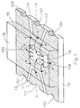
- the dual-mode microwave/millimeter wave IC package structure of the invention can be illustrated by the top view shown in Fig. 1, the bottom view shown in Fig. 2, and the sectional view shown in Fig. 3.
- the top view in Fig. 1 shows that the top surface of the invention includes: an upper left metal strip 11 and an upper right metal strip 12, a left insulating strip 13 and a right insulating strip 14, an upper middle metal area 15, an IC chip 16, an encapsulant 17 and an injection mold 18.
- the upper left metal strip 11 and the upper right metal strip 12 are distributed in zonal area which extend a distance from the substantially central site of the left and right edges of the top surface toward the center of the top surface respectively; besides, the upper left metal strip 11 and the upper right metal strip 12 are connected to the bottom surface through the via holes 111 and 121 positioned at the left and right edge of the top surface, respectively.
- the left insulating strip 13 and the right insulating strip 14 are located outside the upper left metal strip 11 and upper right metal strip 12, both of them are spindling and with tiny area.
- the upper middle metal area 15 is located on the region of the top surface other than the upper left metal strip 11, the upper right metal strip 12, the left insulating strip 13, and the right insulating strip 14; besides, the upper middle metal area 15 is connected to the bottom surface through the via holes 151 ⁇ 156 which are positioned in the upper and lower sides of left edge of the top surface, the upper and lower sides of right edge of the top surface, and the substantially central portion in horizontal direction, respectively.
- the IC chip 16 is placed on the substantially central site, the complete area covered by the IC chip 16 falls into the upper middle metal area 15 without blanketing any via hole, the signal terminals 161 ⁇ 162 and the ground terminals 163 ⁇ 168 are located on the top surface of the chip 16, and these terminals are connected to the upper left metal strip 11, upper right metal strip 12, and upper middle metal area 15 through a plurality of bond wires, respectively.
- the encapsulant 17 (refer to Fig. 3) covers the IC chip 16 and the bond wires to fix the IC chip 16.
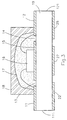
- the injection mold 18 is formed above the encapsulant 17; besides, a substrate 19 is placed between the top surface and the bottom surface.
- the bottom view in Fig. 2 shows that the bottom surface includes: lower left metal strips 21 ⁇ 23, lower right metal strips 24 ⁇ 26, and a lower middle metal area 27.
- the lower left metal strips 21 ⁇ 23 are distributed in zonal areas which extend a distance from the lower, middle, and upper side of the left edge of the bottom surface to the right side of the bottom surface, these metal strips are connected to the upper middle metal area 15, the upper left metal strip 11, and the upper middle metal area 15 through via the holes 151, 111, and 152, respectively.
- the lower right metal strips 24 ⁇ 26 are distributed in zonal areas which extend a distance from the lower, middle, and upper side of the right edge of the bottom surface to the left side of the bottom surface, these metal strips are connected to the upper middle metal area 15, the upper right metal strip 12, and the upper middle metal area 15 through the via holes 153, 121, and 154, respectively.
- the lower middle metal area 27 is located on the substantially central site between the upper edge and the lower edge, and is connected to the upper middle metal area 15 through the via holes 156 and 155.
- the IC package according to the present invention is connected to the exterior microwave/millimeter wave IC in a surface mounting manner, and is adapted to the development of mass production technology. Therefore, when exterior coupling circuits are designed as microstrip mode, operation can be proceeded under microstrip mode by using the IC package according to the present invention.
- the IC package according to the present invention shown in Fig. 1 is placed on the exterior circuit shown in Fig. 4. Since the microstrip 31 contacts with the metal strip 22 of Fig. 2 directly (by soldering, for example), microwave signal vertically ascends from the metal strip 22 (Fig. 2) to the metal strip 11 (Fig. 1) through the via hole 111 when input signals are introduced from the exterior microwave circuit with microstrip 31 (Fig. 4). Reverse ground return current supporting microstrip mode flows from the system ground (30 in Fig.
- Microwave signal flows from front edge 161' of the metal strip 11 to the signal input terminal 161 of the IC 16 through one or more bond wires.
- Bond wire 162-162' is similar to the bond wire 161-161' and thus the description is omitted. Bond wires which are outwardly connected from ground terminals 163 ⁇ 168 of the IC 16 can be classfied into two categories:
- a substantially continuous and complete microstrip transmission line system is formed from the signal input terminal when the microstrip operation mode is used, the excellent ground surface 15 and two different categories of ground wires together with the IC 16 establish an excellent ground loop.
- the external circuit when the external circuit is composed of the coplanar waveguide, the external circuit can be illustrated by Fig. 5, which includes : a substrate 40, a metal plate 42, a medium layer 41, and metal strips 43 ⁇ 48.
- the medium layer 41 can be filled with dielectric material, or kept empty such that the substrate 40 is suspended above the metal plate 42 to form a suspended coplanar waveguide; or the substrate 40 may be immediately adjacent to the metal plate 42 to form a conductor-backed coplanar waveguide.
- the IC package according to the present invention can accept the signals at the input or output of both suspended coplanar waveguide and conductor-backed coplanar waveguide, here the suspended coplanar waveguide is used for illustration : in Fig. 5, signals inputting to and outputting from the ground-signal-ground coplanar waveguide formed by coplanar metal strips 43-44-45 and 46-47-48 are through the substrate 40. Ends 431-441-451 and 461-471-481 of these coplanar metal strips contact with different portions 21-22-23 and 24-25-26 of the bottom surface of the IC package according to the present invention (Fig. 2) by, for example, soldering. Input signals to the coplanar waveguide pass through 441 (Fig. 5) and ascend to the metal strip 11 (Fig.
- Fig. 6 shows another IC package of the invention, the so-called flip-chip, formed by modifying the IC package shown in Fig. 1.
- IC 16 upside down at first, both the signal terminal and the ground terminal are located on the bottom surface.
- the width of metal strips 11 and 12 are lengthened in a-a' direction such that the central portion of the area covered by the IC 16 is located on the metal area 15, the left side of said area is located on the metal strip 11, the right side is located on the metal strip 12, and no via hole is covered by the IC 16.
- the signal input terminal of IC 16 contacts with the metal strip 11, the signal output terminal contacts with the metal strip 12, and all the ground terminals contact with the metal area 15; the portion on metal area 15 which is covered by the IC 16 is properly etched to prevent the surface circuit of IC 16 from short-circuiting.
- the flip-chip not only retrenches bond wires but also avoids the aforesaid slight discontinuity, thus shows better transfer characteristics.
- Figs. 7 and 8 show the experimental results of the IC package according to the present invention, wherein the substrate used has a size of 2.5 mm x 3.2 mm. Specifically, the two-port scattering parameter values (dB) under microstrip mode and coplanar waveguide mode are shown in Figs. 7 and 8, respectively. Notice that the input terminals and output terminals of IC 16 are connected under the "through line" condition. Taking Fig. 1 as an example, the signal terminals 161 and 162 is connected by a shortest line (short-circuit), and the ground terminal pairs (163, 167), (167, 165), (164, 168), and (168, 166) are also connected by the shortest lines, respectively.
- microwave package characteristics include : (1) the input terminal reflection coefficient S 11 is below -15 dB within the operating frequency range up to 30 GHz, which means that the reflected signal is quite little; (2) the transmission coefficient S 21 remains higher than -1 dB within the operating frequency range up to 30 GHz, which means that most of the signal has been faithfully transmitted through the IC 16.
- the transmission loss under microstrip mode is a little more than that under the coplanar waveguide mode. It is confirmed experimentally that the IC package according to the present invention can successfully adopt both microstrip and coplanar waveguide modes within a very wide frequency range (up to 30 GHz) as shown in Figs. 7 and 8.
- a typical 0.25 ⁇ m GaAs PHEMT (Pseudomorphic High Electron Mobility Transistor) is used as the IC 16 which is inserted into the substrate with the aforesaid size, the common-source two-port discrete parameter is examined, the measured scattering parameters are then converted into the maximum gain value G max.
- Fig. 9 shows the G max curve with respect to frequency, the slope of the curve corresponds to the theoretical value of -6 dB/octave, extending the curve by extrapolation also shows that the f max is nearly 35 GHz corresponding to G max of 0 dB. This shows that the IC package according to the present invention can work well with the existing microwave/millimeter wave semiconductor extending the operating frequency up to millimeter band after packaging.
Landscapes
- Engineering & Computer Science (AREA)
- Computer Hardware Design (AREA)
- Microelectronics & Electronic Packaging (AREA)
- Power Engineering (AREA)
- Physics & Mathematics (AREA)
- Condensed Matter Physics & Semiconductors (AREA)
- General Physics & Mathematics (AREA)
- Semiconductor Integrated Circuits (AREA)
- Non-Reversible Transmitting Devices (AREA)
- Microwave Amplifiers (AREA)
Priority Applications (3)
| Application Number | Priority Date | Filing Date | Title |
|---|---|---|---|
| DE0948049T DE948049T1 (de) | 1998-03-03 | 1998-03-03 | Gehäuse für integrierte Mikrowellen- oder Millimeterwellen-Schaltung im Zweifachmodus |
| EP98103731A EP0948049A1 (de) | 1998-03-03 | 1998-03-03 | Gehäuse für integrierte Mikrowellen- oder Millimeterwellen-Schaltung im Zweifachmodus |
| CA002231635A CA2231635C (en) | 1998-03-03 | 1998-03-05 | Dual-mode micrometer/millimeter wave integrated circuit package |
Applications Claiming Priority (2)
| Application Number | Priority Date | Filing Date | Title |
|---|---|---|---|
| EP98103731A EP0948049A1 (de) | 1998-03-03 | 1998-03-03 | Gehäuse für integrierte Mikrowellen- oder Millimeterwellen-Schaltung im Zweifachmodus |
| CA002231635A CA2231635C (en) | 1998-03-03 | 1998-03-05 | Dual-mode micrometer/millimeter wave integrated circuit package |
Publications (1)
| Publication Number | Publication Date |
|---|---|
| EP0948049A1 true EP0948049A1 (de) | 1999-10-06 |
Family
ID=33435760
Family Applications (1)
| Application Number | Title | Priority Date | Filing Date |
|---|---|---|---|
| EP98103731A Withdrawn EP0948049A1 (de) | 1998-03-03 | 1998-03-03 | Gehäuse für integrierte Mikrowellen- oder Millimeterwellen-Schaltung im Zweifachmodus |
Country Status (3)
| Country | Link |
|---|---|
| EP (1) | EP0948049A1 (de) |
| CA (1) | CA2231635C (de) |
| DE (1) | DE948049T1 (de) |
Cited By (3)
| Publication number | Priority date | Publication date | Assignee | Title |
|---|---|---|---|---|
| WO2001052325A1 (en) * | 2000-01-13 | 2001-07-19 | Alpha Industries, Inc. | Microwave ic package with dual mode wave guide |
| WO2006004921A2 (en) * | 2004-06-30 | 2006-01-12 | Honeywell International Inc. | Micro-castellated interposer |
| CN112886234A (zh) * | 2021-01-19 | 2021-06-01 | 南通大学 | 一种基于嵌入式结构的微波毫米波共面共口径天线 |
Citations (5)
| Publication number | Priority date | Publication date | Assignee | Title |
|---|---|---|---|---|
| EP0117434A1 (de) * | 1983-01-28 | 1984-09-05 | Microwave Semiconductor Corp. | Hybrides Mikrowellenteilsystem |
| EP0362161A2 (de) * | 1988-09-29 | 1990-04-04 | Microwave Power, Inc. | Verfahren zum Herstellen eines Substrates für integrierte Mikrowellen-Schaltungen |
| US5235208A (en) * | 1991-02-07 | 1993-08-10 | Mitsubishi Denki Kabushiki Kaisha | Package for microwave integrated circuit |
| EP0627765A1 (de) * | 1993-05-18 | 1994-12-07 | Laboratoires D'electronique Philips S.A.S. | Halbleiteranordnung mit einem Halbleiterelement von Flip-Chip-Typ |
| DE19709541A1 (de) * | 1996-05-23 | 1997-11-27 | Mitsubishi Electric Corp | Hochfrequenzhalbleitervorrichtung |
-
1998
- 1998-03-03 EP EP98103731A patent/EP0948049A1/de not_active Withdrawn
- 1998-03-03 DE DE0948049T patent/DE948049T1/de active Pending
- 1998-03-05 CA CA002231635A patent/CA2231635C/en not_active Expired - Fee Related
Patent Citations (5)
| Publication number | Priority date | Publication date | Assignee | Title |
|---|---|---|---|---|
| EP0117434A1 (de) * | 1983-01-28 | 1984-09-05 | Microwave Semiconductor Corp. | Hybrides Mikrowellenteilsystem |
| EP0362161A2 (de) * | 1988-09-29 | 1990-04-04 | Microwave Power, Inc. | Verfahren zum Herstellen eines Substrates für integrierte Mikrowellen-Schaltungen |
| US5235208A (en) * | 1991-02-07 | 1993-08-10 | Mitsubishi Denki Kabushiki Kaisha | Package for microwave integrated circuit |
| EP0627765A1 (de) * | 1993-05-18 | 1994-12-07 | Laboratoires D'electronique Philips S.A.S. | Halbleiteranordnung mit einem Halbleiterelement von Flip-Chip-Typ |
| DE19709541A1 (de) * | 1996-05-23 | 1997-11-27 | Mitsubishi Electric Corp | Hochfrequenzhalbleitervorrichtung |
Cited By (5)
| Publication number | Priority date | Publication date | Assignee | Title |
|---|---|---|---|---|
| WO2001052325A1 (en) * | 2000-01-13 | 2001-07-19 | Alpha Industries, Inc. | Microwave ic package with dual mode wave guide |
| WO2006004921A2 (en) * | 2004-06-30 | 2006-01-12 | Honeywell International Inc. | Micro-castellated interposer |
| WO2006004921A3 (en) * | 2004-06-30 | 2006-09-21 | Honeywell Int Inc | Micro-castellated interposer |
| US7507914B2 (en) | 2004-06-30 | 2009-03-24 | Honeywell International Inc. | Micro-castellated interposer |
| CN112886234A (zh) * | 2021-01-19 | 2021-06-01 | 南通大学 | 一种基于嵌入式结构的微波毫米波共面共口径天线 |
Also Published As
| Publication number | Publication date |
|---|---|
| CA2231635C (en) | 2001-05-15 |
| DE948049T1 (de) | 2000-08-17 |
| CA2231635A1 (en) | 1999-09-05 |
Similar Documents
| Publication | Publication Date | Title |
|---|---|---|
| JP3500268B2 (ja) | 高周波用入出力端子ならびにそれを用いた高周波用半導体素子収納用パッケージ | |
| US6573803B1 (en) | Surface-mounted millimeter wave signal source with ridged microstrip to waveguide transition | |
| US5235300A (en) | Millimeter module package | |
| US5138436A (en) | Interconnect package having means for waveguide transmission of rf signals | |
| EP0977298B1 (de) | Hochfrequenzmodul | |
| JPH05266808A (ja) | 空中経路によって補償されたマイクロ波装置 | |
| EP1081989B1 (de) | Hochfrequenzschaltungsplatte und seine Verbindungsstruktur | |
| US5783847A (en) | Dual-mode micrometer/millimeter wave integrated circuit package | |
| US6140698A (en) | Package for microwave and mm-wave integrated circuits | |
| CA2231635C (en) | Dual-mode micrometer/millimeter wave integrated circuit package | |
| US6781488B2 (en) | Connected construction of a high-frequency package and a wiring board | |
| US8829659B2 (en) | Integrated circuit | |
| JP3305589B2 (ja) | 高周波用半導体装置の実装構造 | |
| WO2002082578A1 (fr) | Structure de connexion de broche connecteur et de ligne de signal et boitier a semi-conducteur utilisant cette structure | |
| JP2001257415A (ja) | 光半導体装置 | |
| JP3618046B2 (ja) | 高周波回路用パッケージ | |
| US5161000A (en) | High-frequency thick-film semiconductor circuit | |
| JP2002359443A (ja) | 高周波パッケ−ジと配線基板との接続構造 | |
| JPH0936617A (ja) | 高周波モジュール | |
| JP3470052B2 (ja) | 高周波用部品の接続構造 | |
| JP3916988B2 (ja) | 高周波モジュール | |
| JP3337016B2 (ja) | 高周波半導体パッケージ | |
| JPH05259717A (ja) | マイクロストリップ結合器 | |
| JP3619397B2 (ja) | 高周波用配線基板および接続構造 | |
| JP2775678B2 (ja) | 高周波半導体集積回路装置 |
Legal Events
| Date | Code | Title | Description |
|---|---|---|---|
| PUAI | Public reference made under article 153(3) epc to a published international application that has entered the european phase |
Free format text: ORIGINAL CODE: 0009012 |
|
| 17P | Request for examination filed |
Effective date: 19980327 |
|
| AK | Designated contracting states |
Kind code of ref document: A1 Designated state(s): DE FR GB |
|
| AX | Request for extension of the european patent |
Free format text: AL;LT;LV;MK;RO;SI |
|
| EL | Fr: translation of claims filed | ||
| AKX | Designation fees paid |
Free format text: DE FR GB |
|
| DET | De: translation of patent claims | ||
| STAA | Information on the status of an ep patent application or granted ep patent |
Free format text: STATUS: THE APPLICATION IS DEEMED TO BE WITHDRAWN |
|
| 18D | Application deemed to be withdrawn |
Effective date: 20041001 |