EP0944959B1 - Verfahren und vorrichtung zur wahl von m-ansteuerungsleitungen unter n-ansteuerungsleitungen - Google Patents
Verfahren und vorrichtung zur wahl von m-ansteuerungsleitungen unter n-ansteuerungsleitungen Download PDFInfo
- Publication number
- EP0944959B1 EP0944959B1 EP97954542A EP97954542A EP0944959B1 EP 0944959 B1 EP0944959 B1 EP 0944959B1 EP 97954542 A EP97954542 A EP 97954542A EP 97954542 A EP97954542 A EP 97954542A EP 0944959 B1 EP0944959 B1 EP 0944959B1
- Authority
- EP
- European Patent Office
- Prior art keywords
- select lines
- selectable
- select
- selectable devices
- devices
- Prior art date
- Legal status (The legal status is an assumption and is not a legal conclusion. Google has not performed a legal analysis and makes no representation as to the accuracy of the status listed.)
- Revoked
Links
Images






Classifications
-
- G—PHYSICS
- G06—COMPUTING OR CALCULATING; COUNTING
- G06F—ELECTRIC DIGITAL DATA PROCESSING
- G06F12/00—Accessing, addressing or allocating within memory systems or architectures
- G06F12/02—Addressing or allocation; Relocation
- G06F12/06—Addressing a physical block of locations, e.g. base addressing, module addressing, memory dedication
Definitions
- the present invention is related to electronics systems and more particularly to the selection of system devices by a system master.
- system controller such as a microprocessor may need to enable another system component or “agent” such as a memory chip in order to gain access to the data stored by the memory chip.
- agent such as a memory chip
- the master and agent devices must typically include additional pins for asserting and accepting selection or enable signals, and there are costs associated with providing semiconductor die space for these pins and supporting circuitry. Similarly, there are costs associated with providing printed circuit (PC) board space for routing the selection or enable signals between the master and agent devices.
- PC printed circuit
- Figure 1 shows a system 10 that implements a prior device selection scheme wherein selection bus 15 transmits a binary encoded identification number from master 20 to select one of agents 21-36 so that master 20 may access the selected agent via data bus 48.
- each of agents 21-36 must be provided with (1) a unique identification number such as I.D. NO. 45 of agent 21 and (2) comparator circuitry 40 for comparing the transmitted identification number to the agent's identification number.
- the width of selection bus 15 is N bits, and master 20 and agents 21-36 must each have N pins dedicated or multiplexed for device selection.
- the number of output pins required for master 20 is minimized according to the scheme of Figure 1; however, the total number of input pins required for agents 21-36 is maximized.
- FIG. 2 shows a system 50 that implements another prior device selection scheme.
- a selection bus 55 transmits a binary encoded identification number (shown as BIT 0 - BIT 3) and its complement (shown as BIT 0 - BIT 3 ) from master 60 to select one of agents 61-76 so that master 60 may access the selected agent via data bus 54.
- the assertion or deassertion of the select signals for the complementary identification number ( BIT 0 - BIT 3 ) directly depends on the value of the true identification number (BIT 0 - BIT 3).
- each of agents 61-76 must be provided with majority logic circuitry such as a logical AND gate 52.
- the width of the selection bus 55 is 2N bits
- master 60 must have 2N output pins for device selection
- agents 61-76 must each have N input pins for device selection.
- Device selection by the system of Figure 2 is typically faster than that of Figure 1 because majority logic circuitry is typically faster than comparators. Furthermore, agents need not be assigned identification numbers. The number of output pins required by the master to support device selection and the number of conductors for the selection bus are both doubled. Therefore, this prior art scheme is typically applied to systems with a limited (e.g. four) number of agents.
- Figure 3 shows a system 80 that implements another prior device selection scheme wherein each of a plurality of enable lines 85 are routed from master 90 to a corresponding one of agents 91-106 so that master 90 may enable and access the selected agent via data bus 115.
- master 90 To support device selection according to this method, master 90 must be provided with a 1-of-16 decoder circuit 110 that accepts a binary number and asserts one of the sixteen enable signals EN1-EN16.
- master 90 In a system supporting a maximum of 2 N agents, master 90 must have a 1-of-N decoder providing 2 N enable signals on 2 N lines. Each of the 2 N agents must have one input pin for device selection. Master 90 must have 2 N output pins for device selection.
- the total number of input pins required for the agent devices is minimized according to the scheme of Figure 3; however, the number of output pins required for the master device is maximized.
- An alternative scheme would place the 1-of-16 decoder circuit 100 external to master 90, thus reducing the number of output pins for device selection by master 90. Providing the 1-of-16 decoder circuit 100 as a separate device would slow the process of device selection by an undesirable amount for some systems.
- Another object of the present invention is to permit the selecting device to select all of the selectable devices simultaneously.
- Another object of the present invention is to select sets of the selectable devices simultaneously.
- the interconnect apparatus includes a plurality of N select lines and a plurality of connections coupling each of the selectable devices to an unique group of the N select lines.
- Each unique group has at least one select line different from the select lines of any other unique group.
- Each unique group also includes M of the N select lines, wherein M is greater than one and less than N.
- the maximum number of the devices may be equal to the total number of the unique groups of the N select lines. Additionally, at least one of the devices may be selected for communication by activating at least one of the unique groups.
- a method for selectively enabling agents or selectable devices of a system using a plurality of N select lines includes the steps of: assigning each agent to a unique group M of the plurality of N select lines, M being greater than 1; translating an identification number into a combinatorial representation that specifies which of the plurality of N select lines are to be asserted; and asserting a first unique group of the plurality of N select lines to select one of the plurality of selectable devices.
- a device selection scheme is described wherein a master (selecting device) selects one of a plurality of X agents (selectable devices) by selectively enabling a plurality M of a total of N select lines.
- Each agent has a distinct subset M of the N select lines that corresponds to that agent. More than one agent can be selected by asserting the select lines that correspond to the respective subsets of select lines for the selected agents. Similarly, all agents may be selected by asserting all N select lines.
- the device selection scheme described below may be used for systems supporting one to X agents, and is well suited for systems supporting in excess of approximately eight to ten agents.
- the device selection scheme is referred to herein as "N choose M," wherein M is greater than one (1) and less than N.
- N choose M is related to the combinatorics theory of mathematics that states that, for a given number of N items, there is a maximum number of X unique combinations of the N items taken M at a time. For example, given a total of six (6) items, there are a total of fifteen (15) unique combinations of two (2) items.
- the number X defines the maximum number of agent devices that can be supported by the system
- the number M defines the number of select lines that are routed to each agent for selection purposes. For one embodiment, M is approximately one-half N.
- the N choose M device selection scheme offers a good compromise between the number of output pins allocated on the master and the number of input pins allocated on each agent for selection purposes. Furthermore, the N choose M device selection scheme eliminates the need to assign unique identification numbers to each device, enables the use of majority logic, and therefore reduces system latency when compared to some prior schemes.
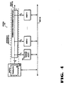
- Figure 4 shows an exemplary system 120 that implements an N choose M device selection scheme wherein N choose M selector 125 is used by master 130 to select one or more of X agents by asserting at least one of a unique subset M of N select lines 135.
- System 120 is a shared communication system, wherein selected agents may communicate data and/or control information with master 130 via bus 140. According to other embodiments, selected devices perform a predetermined task in response to being selected.
- N choose M selector 125 includes translator 145 and combinatorial interconnect matrix 150.
- Translator 145 translates an identification number into a combinatorial representation that specifies which of the N select lines 35 are to be asserted.
- Translator 145 may translate binary, hexadecimal, BCD, or an identification number in any other format to a combinatorial representation.
- translator 145 may comprise combinatorial logic.
- translator 145 may comprise a table(s) that stores translation information.
- translator 145 may comprise software routines that perform the translation function and are coupled to hardware to output the combinatorial representation on specific N select lines 135.
- Combinatorial interconnect matrix 150 couples each agent to a unique subset M of the N select lines 135.
- Agent 1 is coupled to subset M 1
- agent 2 is coupled to subset M 2
- up to agent X coupled to subset M X .
- Each agent is provided with majority logic 155, which may be, but is not limited to, a logical AND gate to determine when its subset of M signal lines are properly asserted.
- One agent may be selected by properly asserting select signals on the requisite M subset of N select lines 135.
- System 120 also enables multiple agents to be simultaneously selected by enabling the proper subsets M of the N select lines 135. Additionally, all X agents may be simultaneously selected by asserting the proper select signals on the N select lines 135.
- assert does not require that all select signals be set to a logic high or a logic low value to “assert” the select line; rather, each select signal be activated to the value expected by the agent in view of the configuration of the majority logic 155 for that agent.
- translator 145 may be provided on the same semiconductor substrate as the master 130. Alternatively, translator 145 may be provided on a different semiconductor substrate or as discrete circuitry that is distinct from the master 130.
- the master 130 is provided with N output pins to support device selection. Regardless, each agent is provided with M input pins to support remote device selection. For some applications, such as when the plurality of agents are registers of a microprocessor, all of the components of system 120 may be provided on a single semiconductor substrate.
- Combinatorial interconnect matrix 215 includes the hardwired connections of agents A1-A15 to select lines A-F.
- Alternative means for coupling A1-A15 to select lines A-F as shown in Figure 5 may be employed including, fuses, diodes, resistors, and other means.
- the translator of system 200 is not shown, but may be internal or external to master 210.
- master 210 asserts the proper select signals on select lines E and F.
- master 210 asserts the proper select signals on select lines D, E, and F.
- master 210 asserts the proper select signals on select lines A-F.
- a designer determines the numbers N and M to accommodate the desired number of agents for the system, wherein the maximum number X of agents supported by a particular system is equal to N ! / [( N - M )! M !].
- Tables 1 and 2 compare examples of the resources required by the N choose M scheme of the present embodiments when compared to the prior art schemes shown in Figures 1-3. Specifically, Table 1 shows the system requirements for implementing a 6 choose 2 scheme for selecting an agent from a maximum of approximately 16 agents (15 agents for Figure 4), and Table 2 shows the system requirements for implementing a 7 choose 3 scheme for selecting an agent from a maximum of approximately 32 agents (35 agents for Figure 4).
- Tables 1 and 2 indicate that the number of inputs and outputs that must be allocated to the master and each agent is a compromise between the prior schemes such that the cost or burden of implementing the present device selection scheme is distributed between master 130, agents A1-AX, and combinatorial interconnect matrix 150.
- Tables 1 and 2 indicate, with the exception of the scheme of prior art Figure 1, the N choose M scheme results in the lowest number of master outputs. Similarly, with the exception of the scheme of prior art Figure 3, the N choose M scheme results in the lowest number of agent inputs.
- Tables 1 and 2 further show that for N choose 2, the product of the number of master outputs (N), the number of agent inputs (M), and the maximum number of agents (X) supported by a device selection scheme is a minimum number for the device selection scheme illustrated in Figure 4 relative to the prior art schemes illustrated in Figures 1-3.
- Figure 6 shows that for systems that support in excess of approximately ten agents, an N choose 2 device selection scheme will yield a product function (N*M*X) that provides a minimum result for a system supporting X agents as compared with the prior art schemes of Figures 1-3.
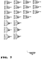
- Figure 7 shows combinatorial translator 250 which is one embodiment of translator 145 in Figure 4.
- Translator 250 is a 6 choose 2 binary-to-combinatorial translator that comprises fifteen (15) four-input logical AND gates 260-274 and six (6) six-input logical OR gates 280-285 for use in the 6 choose 2 system 200 of Figure 5.
- Each of the AND gates 260-274 is coupled to receive four binary bits (d3, d2, d1, and d0) that correspond to sixteen possible identification numbers. As shown, each of the AND gates 260-274 has its inputs configured such that it will output a logic 1 only in response to a specific identification number.
- the outputs of the AND gates 260-274 are coupled to the inputs of the OR gates 280-285 in the manner shown such that the assertion of the output of one of the AND gates 260-274 results in two of the select lines A-F being asserted to select a corresponding agent.
- Each OR gate is also shown as including an "ALL" input that causes all of the select signals A-F to be asserted when the "ALL" signal is asserted.
- Figure 8 shows system 300 that implements another device selection scheme.
- System 300 includes Y choose Z selector 325 and W choose R selector 360, each having an N choose M configuration as illustrated in Figure 4.
- Y choose Z selector 325 enables selection of up to V devices, wherein V is equal to Y ! / [( Y - Z )! Z !].
- W choose R selector 360 enables selection of up to U devices, wherein U is equal to W ! / [( W - R )! R !].
- system 300 supports the selection of one or more of V x U agents by asserting at least one unique subset Z of Y select lines 335 and/or at least one unique subset R of W select lines 370.
- System 300 is a shared communication system, wherein selected agents may communicate data and/or control information with master 330 via bus 340. According to other embodiments, selected devices perform a predetermined task in response to being selected.
- Y choose Z selector 325 includes translator 345 and combinatorial interconnect matrix 350.
- W choose R selector includes translator 345 and combinatorial interconnect matrix 365.
- Translator 345 translates a first identification number into a combinatorial representation that specifies which of the Y select lines 335 are to be asserted.
- Translator 345 also translates a second identification number into a combinatorial representation that specifies which of the W select line 370 are to be asserted.
- Translator 345 may translate binary, hexadecimal, BCD, or identification numbers in any other format to a combinatorial representation.
- translator 345 may comprise combinatorial logic.
- translator 345 may comprise a tables(s) that stores translation information.
- translator 345 may comprise software routines that perform the translation functions and are coupled to hardware to output the combinatorial representation on specific Y and W select lines.
- translator 345 may comprise two translators, namely: a first translator coupled to combinatorial interconnect matrix 350, translating the first identification number, and asserting the Y select lines 335; and a second translator coupled to combinatorial interconnect matrix 365, translating the second identification number, and asserting the W select lines 370.
- Combinatorial interconnect matrix 350 couples each column of agents to a unique subset Z of the Y select lines 335.
- combinatorial interconnect matrix 365 couples each row of agents to unique subset R of the W select lines 370.
- Agents 1-1 through 1-U are coupled to subset Z 1
- agents 2-1 through 2-U are coupled to subset Z 2 , up to agents V-1 through V-U coupled to subset Z V .
- agents 1-1 through V-1 are coupled to subset R 1
- agents 1-2 through V-2 are coupled to subset R 2 up to agents 1-U through V-U coupled to subset R V .
- Each agent includes majority logic 355 as illustrated in agent 1-1.
- Majority logic 355 may be, but is not limited to, a logical AND gate to determine when the appropriate subset of select lines is asserted for a particular agent.
- One agent may be selected by properly asserting select signals on the requisite Z subset of Y select lines 335 and the requisite R subset of W select lines 370.
- System 300 may also enable multiple agents to be simultaneously selected by enabling the proper subsets Z of Y select lines 335 and/or the proper subset R of W select lines 370. For example, an entire row or column of agents may be simultaneously selected. Additionally, all V x U agents may be simultaneously selected by asserting the proper select signals on Y select lines 335 and W select lines 370.
- a comparable system comprising a device selection scheme implementing (Y + W) choose (Z + R).
- Y + W device selection scheme
- Z + R device selection scheme
- an 8 choose 4 system using one interconnect matrix according to Figure 4 supports 70 selectable agents.
- a comparable system including two 4 choose 2 matrices according to Figure 8 supports (6 x 6) 36 selectable agents.
- system 300 may be desirable to employ system 300 over a device selection scheme implementing (Y + W) choose (Z + R) or other one interconnect matrix systems according to Figure 4.
- a device selection scheme implementing (Y + W) choose (Z + R) or other one interconnect matrix systems according to Figure 4.
- the encoding in the master would be simpler (i.e., the hardware or software of translator 345 would be simpler) or there would be a pin savings on the master device compared to other alternatives.
- two 4 choose 2 matrices may select one or more of 36 devices using the configuration of system 300.
- an 8 choose 4 system using only one interconnect matrix according to Figure 4 supports up to 70 selectable devices, but may require more complex encoding hardware for translator 145 (relative to translator 345).
- an 9 choose 2 system using only interconnect matrix according to Figure 4 may be used to support up to 36 selectable devices.
- This alternative has the disadvantage of requiring nine pins on the master device as opposed to 8 pins on the master device using two 4 choose 2 matrices according to system 300. The number of pins on the master devices may be important for some systems.
- Figure 9 shows system 400 that is one embodiment of system 300 having two interconnect matrices each supporting 3 choose 2 device selection schemes.
- System 400 includes master 430, combinatorial interconnect matrix 425, combinatorial interconnect matrix 465, and agents 1-1 through 3-3.
- Master 430 is capable of selecting one or more of up to nine (9) agents via select lines A-F.
- the translator of system 300 is not shown, but may be internal or external to master 430.
- Combinatorial interconnect matrix 425 includes hardwired connections for agents 1-1 through 3-3.
- the first column of agents 1-1 through 1-3 is coupled select lines A and B.
- the second column of agents 2-1 through 2-3 is coupled to select lines A and C.
- the third column of agents 3-1 through 3-3 is coupled to select lines B and C.
- Combinatorial interconnect matrix 465 includes hardwired connections for agents 1-1 through 3-3.
- the first row of agents 1-1 through 3-1 is coupled to select lines D and E.
- the second row of agents 1-2 through 1-3 is coupled to select lines D and F.
- the third row of agents 1-3 through 3-3 is coupled to select lines E and F.
- any individual agent may be selected.
- master 430 asserts the proper select signals on select lines A, B, D, and E.
- master 430 asserts the proper select signals on select lines A-E.
- master 430 asserts the proper select signals on select lines A, B, D, E, and F.
- master 430 asserts the proper select signal on select lines A-E.
- System 400 support up to (3 x 3) 9 selectable agents.
- a comparable 6 choose 4 system according to Figure 4 would support up to 15 selectable agents.
Landscapes
- Engineering & Computer Science (AREA)
- Theoretical Computer Science (AREA)
- Physics & Mathematics (AREA)
- General Engineering & Computer Science (AREA)
- General Physics & Mathematics (AREA)
- Multi Processors (AREA)
- Hardware Redundancy (AREA)
- Small-Scale Networks (AREA)
Claims (22)
- Verbindungsvorrichtung zum Auswählen wenigstens einer von einer Mehrzahl von auswählbaren Einrichtungen zur Kommunikation, die aufweist:wobei eine maximale Anzahl der Mehrzahl von auswählbaren Einrichtungen gleich einer Gesamtzahl von einzigartigen Gruppen der Mehrzahl von N Auswahlleitungen ist; undeine Mehrzahl von N Auswahlleitungen;eine Mehrzahl von Verbindungen zum Koppeln von jeder der Mehrzahl von auswählbaren Einrichtungen zu einer einzigartigen Gruppe der Mehrzahl von N Auswahlleitungen, wobei jede einzigartige Gruppe wenigstens eine Auswahlleitung aufweist, die von den Auswahlleitungen von jeder der anderen einzigartigen Gruppe unterschiedlich ist, und wobei jede einzigartige Gruppe M der Mehrzahl von N Auswahlleitungen aufweist, wobei M größer ist als eins und kleiner ist als N;
wobei die wenigstens eine Einrichtung zur Kommunikation durch Aktivieren wenigstens einer der einzigartigen Gruppen auswählbar ist. - Vorrichtung nach Anspruch 1, wobei die maximale Anzahl der Mehrzahl von auswählbaren Einrichtungen gleich N! / [(N-M)!M!] ist.
- Vorrichtung nach Anspruch 1 oder 2, wobei mehr als eine, jedoch nicht alle der Mehrzahl von auswählbaren Einrichtungen zur Kommunikation simultan auswählbar sind.
- Vorrichtung nach Anspruch 1 oder 2, wobei alle der Mehrzahl von auswählbaren Einrichtungen zur Kommunikation simultan auswählbar sind.
- System, das aufweist:eine erste Verbindungsvorrichtung, welche die Verbindungsvorrichtung nach Anspruch 1 aufweist, wobei die erste Verbindungsvorrichtung zur Auswahl einer Teilmenge der Mehrzahl von auswählbaren Einrichtungen dient;eine zweite Verbindungsvorrichtung zum Auswählen von wenigstens einer der Teilmenge der Mehrzahl von auswählbaren Einrichtungen, wobei die zweite Verbindungsvorrichtung aufweist:eine Mehrzahl von Y Auswahlleitungen;eine weitere Mehrzahl von Verbindungen zum Koppeln jeder der Mehrzahl von auswählbaren Einrichtungen zu einer einzigartigen Gruppe der Mehrzahl von Y Auswahlleitungen, wobei jede einzigartige Gruppe der Mehrzahl von Y Auswahlleitungen wenigstens eine Auswahlleitung aufweist, die sich von jeder der anderen einzigartigen Gruppe unterscheidet, und wobei jede einzigartige Gruppe der Mehrzahl von Y Auswahlleitungen Z der Mehrzahl von Y Auswahlleitungen aufweist, wobei Z größer als eins und kleiner als Y ist.
- System nach Anspruch 5, das aufweist:einen Master, der eine Mehrzahl von N Ausgängen aufweist, die mit der Mehrzahl von N Auswahlleitungen gekoppelt sind, und eine Mehrzahl von Y Ausgängen, die mit der Mehrzahl von Y Auswahlleitungen gekoppelt sind.
- System nach Anspruch 5 oder 6, wobei die maximale Anzahl der Mehrzahl von auswählbaren Einrichtungen gleich N! / [(N-M)!M!] multipliziert mit Y! / [(Y-Z)!Y!] ist.
- System nach einem der Ansprüche 5 bis 7, das ferner aufweist:eine Schaltung innerhalb wenigstens einer der Mehrzahl von auswählbaren Einrichtungen zum Erfassen, wann wenigstens eine der einzigartigen Gruppen von M Auswahlleitungen und wenigstens eine der einzigartigen Gruppen von Z Auswahlleitungen aktiviert ist, so dass die wenigstens eine der Mehrzahl von auswählbaren Einrichtungen ausgewählt wird.
- System, das aufweist:eine Verbindungsvorrichtung nach einem der Ansprüche 1 bis 4;die Mehrzahl von auswählbaren Einrichtungen; undeinen Umsetzer, der eine Identifikationsnummer in eine kombinatorische Darstellung umsetzt, die eine der einzigartigen Gruppen der Mehrzahl von N Auswahlleitungen spezifiziert, die festzulegen ist, um eine der Mehrzahl von auswählbaren Einrichtungen in Abhängigkeit von der kombinatorischen Darstellung zu aktivieren.
- System nach Anspruch 9, das ferner einen Master aufweist, der mit dem Umsetzer gekoppelt ist und die Identifikationsnummer bereitstellt.
- System nach Anspruch 9, das ferner einen Master aufweist, der den Umsetzer einschließt und die Identifikationsnummer bereitstellt.
- System nach einem der Ansprüche 9 bis 11, wobei der Übersetzer, die Verbindungsvorrichtung und eine der Mehrzahl von auswählbaren Einrichtungen auf einem einzigen Halbleitersubstrat gebildet sind.
- System nach einem der Ansprüche 9 bis 12, wobei die Identifikationsnummer mehr als eine der Mehrzahl von auswählbaren Einrichtungen anzeigt, wobei der Umsetzer mehr als eine der einzigartigen Gruppen der Mehrzahl von N Auswahlleitungen festlegt, um mehr als eine der Mehrzahl von auswählbaren Einrichtungen zu aktivieren.
- System nach einem der Ansprüche 9 bis 13, das ferner aufweist:eine Schaltung innerhalb einer der Mehrzahl von auswählbaren Einrichtungen zum Erfassen, wenn wenigstens eine einzigartige Gruppe der Mehrzahl von N Auswahlleitungen aktiviert wird, so dass die wenigstens eine der Mehrzahl von auswählbaren Einrichtungen ausgewählt wird.
- System nach einem der Ansprüche 9 bis 14, wobei die Mehrzahl von auswählbaren Einrichtungen auswählbare Speichereinrichtungen aufweist.
- System, das aufweist:eine Verbindungsvorrichtung nach einem der Ansprüche 1 bis 4 oder ein System nach einem der Ansprüche 5 bis 15; undeinen Master der eine Mehrzahl von N Auswahlausgängen aufweist, die mit den N Auswahlleitungen gekoppelt sind.
- Steuerungseinrichtung, die aufweist:eine Mehrzahl von N Ausgängen;eine Umsetzerschaltung, die mit der Mehrzahl von N Ausgängen gekoppelt ist, wobei:die Umsetzerschaltung eine Identifikationsnummer in eine kombinatorische Darstellung umsetzt, die spezifiziert, welche der Mehrzahl von N Ausgängen festzulegen sind;den festgelegten N Ausgängen jeweils wenigstens M Ausgängen festgelegt werden, wobei M größer ist als eins; unddie Steuerungseinrichtung in der Lage ist, wenigstens eine der Mehrzahl von auswählbaren Einrichtungen über eine Vorrichtung nach einem der Ansprüche 1 bis 4 oder einem System nach einem der Ansprüche 5 bis 16 auszuwählen.
- Verfahren zum Auswählen zwischen einer Mehrzahl von auswählbaren Einrichtungen mittels einer Vorrichtung nach einem der Ansprüche 1 bis 4 oder einem System nach einem der Ansprüche 5 bis 16, das die Schritte aufweist:Zuweisen jeder auswählbaren Einrichtung zu einer einzigartigen Gruppe von M der Mehrzahl von N Auswahlleitungen, wobei M größer ist als eins; undFestlegen einer ersten einzigartigen Gruppe aus der Mehrzahl von N Auswahlleitungen, um eine erste der Mehrzahl von auswählbaren Einrichtungen auszuwählen.
- Verfahren nach Anspruch 18, das ferner den Schritt aufweist:Festlegen einer zweiten einzigartigen Gruppe der Mehrzahl von N Auswahlleitungen, die mit einer zweiten auswählbaren Einrichtung korrespondiert, um gleichzeitig die ersten und zweiten auswählbaren Einrichtungen auszuwählen.
- Verfahren nach Anspruch 18 oder 19, das ferner den Schritt aufweist:Festlegen aller der Mehrzahl von N Auswahlleitungen, um gleichzeitig alle der Mehrzahl von auswählbaren Einrichtungen auszuwählen.
- Verfahren nach einem der Ansprüche 18 bis 20, wobei eine maximale Anzahl der Mehrzahl von auswählbaren Einrichtungen gleich N! / [(N-M)!M!] ist.
- Verfahren nach einem der Ansprüche 18 bis 21, das ferner den Schritt aufweist:Umsetzen einer Identifikationsnummer in eine kombinatorische Darstellung, die spezifiziert, welche der Mehrzahl von N Auswahlleitungen festzulegen sind.
Applications Claiming Priority (3)
| Application Number | Priority Date | Filing Date | Title |
|---|---|---|---|
| US08/767,739 US5995016A (en) | 1996-12-17 | 1996-12-17 | Method and apparatus for N choose M device selection |
| US767739 | 1996-12-17 | ||
| PCT/US1997/022500 WO1998027650A2 (en) | 1996-12-17 | 1997-12-10 | Method and apparatus for n choose m device selection |
Publications (2)
| Publication Number | Publication Date |
|---|---|
| EP0944959A2 EP0944959A2 (de) | 1999-09-29 |
| EP0944959B1 true EP0944959B1 (de) | 2004-04-07 |
Family
ID=25080413
Family Applications (1)
| Application Number | Title | Priority Date | Filing Date |
|---|---|---|---|
| EP97954542A Revoked EP0944959B1 (de) | 1996-12-17 | 1997-12-10 | Verfahren und vorrichtung zur wahl von m-ansteuerungsleitungen unter n-ansteuerungsleitungen |
Country Status (6)
| Country | Link |
|---|---|
| US (1) | US5995016A (de) |
| EP (1) | EP0944959B1 (de) |
| AU (1) | AU5896798A (de) |
| DE (1) | DE69728559T2 (de) |
| GB (1) | GB9913305D0 (de) |
| WO (1) | WO1998027650A2 (de) |
Families Citing this family (60)
| Publication number | Priority date | Publication date | Assignee | Title |
|---|---|---|---|---|
| US6157968A (en) * | 1998-01-26 | 2000-12-05 | Motorola Inc. | Interface with selector receiving control words comprising device identifiers for determining corresponding communications parameter set for interface port transfer of data words to peripheral devices |
| GB2456743A (en) * | 2007-07-16 | 2009-07-29 | Thorn Security | Searching identity space for devices connected to a bus using masks and increasing mask length when replies collide |
| US9288089B2 (en) | 2010-04-30 | 2016-03-15 | Ecole Polytechnique Federale De Lausanne (Epfl) | Orthogonal differential vector signaling |
| US9362962B2 (en) | 2010-05-20 | 2016-06-07 | Kandou Labs, S.A. | Methods and systems for energy-efficient communications interface |
| US9083576B1 (en) | 2010-05-20 | 2015-07-14 | Kandou Labs, S.A. | Methods and systems for error detection and correction using vector signal prediction |
| US9288082B1 (en) | 2010-05-20 | 2016-03-15 | Kandou Labs, S.A. | Circuits for efficient detection of vector signaling codes for chip-to-chip communication using sums of differences |
| US9564994B2 (en) | 2010-05-20 | 2017-02-07 | Kandou Labs, S.A. | Fault tolerant chip-to-chip communication with advanced voltage |
| US9596109B2 (en) | 2010-05-20 | 2017-03-14 | Kandou Labs, S.A. | Methods and systems for high bandwidth communications interface |
| US9300503B1 (en) | 2010-05-20 | 2016-03-29 | Kandou Labs, S.A. | Methods and systems for skew tolerance in and advanced detectors for vector signaling codes for chip-to-chip communication |
| US8539318B2 (en) | 2010-06-04 | 2013-09-17 | École Polytechnique Fédérale De Lausanne (Epfl) | Power and pin efficient chip-to-chip communications with common-mode rejection and SSO resilience |
| US9106220B2 (en) | 2010-05-20 | 2015-08-11 | Kandou Labs, S.A. | Methods and systems for high bandwidth chip-to-chip communications interface |
| US9251873B1 (en) | 2010-05-20 | 2016-02-02 | Kandou Labs, S.A. | Methods and systems for pin-efficient memory controller interface using vector signaling codes for chip-to-chip communications |
| US9479369B1 (en) | 2010-05-20 | 2016-10-25 | Kandou Labs, S.A. | Vector signaling codes with high pin-efficiency for chip-to-chip communication and storage |
| US9246713B2 (en) | 2010-05-20 | 2016-01-26 | Kandou Labs, S.A. | Vector signaling with reduced receiver complexity |
| US8649445B2 (en) | 2011-02-17 | 2014-02-11 | École Polytechnique Fédérale De Lausanne (Epfl) | Methods and systems for noise resilient, pin-efficient and low power communications with sparse signaling codes |
| US9450744B2 (en) | 2010-05-20 | 2016-09-20 | Kandou Lab, S.A. | Control loop management and vector signaling code communications links |
| US9077386B1 (en) | 2010-05-20 | 2015-07-07 | Kandou Labs, S.A. | Methods and systems for selection of unions of vector signaling codes for power and pin efficient chip-to-chip communication |
| US9106238B1 (en) | 2010-12-30 | 2015-08-11 | Kandou Labs, S.A. | Sorting decoder |
| US8593305B1 (en) | 2011-07-05 | 2013-11-26 | Kandou Labs, S.A. | Efficient processing and detection of balanced codes |
| US9401828B2 (en) | 2010-05-20 | 2016-07-26 | Kandou Labs, S.A. | Methods and systems for low-power and pin-efficient communications with superposition signaling codes |
| US9667379B2 (en) | 2010-06-04 | 2017-05-30 | Ecole Polytechnique Federale De Lausanne (Epfl) | Error control coding for orthogonal differential vector signaling |
| US9275720B2 (en) | 2010-12-30 | 2016-03-01 | Kandou Labs, S.A. | Differential vector storage for dynamic random access memory |
| US9268683B1 (en) | 2012-05-14 | 2016-02-23 | Kandou Labs, S.A. | Storage method and apparatus for random access memory using codeword storage |
| CN104995612B (zh) | 2013-01-17 | 2020-01-03 | 康杜实验室公司 | 低同步开关噪声芯片间通信方法和系统 |
| WO2014172377A1 (en) | 2013-04-16 | 2014-10-23 | Kandou Labs, S.A. | Methods and systems for high bandwidth communications interface |
| CN105393512B (zh) | 2013-06-25 | 2019-06-28 | 康杜实验室公司 | 具有低接收器复杂度的向量信令 |
| US9106465B2 (en) | 2013-11-22 | 2015-08-11 | Kandou Labs, S.A. | Multiwire linear equalizer for vector signaling code receiver |
| US9806761B1 (en) | 2014-01-31 | 2017-10-31 | Kandou Labs, S.A. | Methods and systems for reduction of nearest-neighbor crosstalk |
| CN105993151B (zh) | 2014-02-02 | 2019-06-21 | 康杜实验室公司 | 低isi比低功率芯片间通信方法和装置 |
| US9369312B1 (en) | 2014-02-02 | 2016-06-14 | Kandou Labs, S.A. | Low EMI signaling for parallel conductor interfaces |
| EP3672176B1 (de) | 2014-02-28 | 2022-05-11 | Kandou Labs, S.A. | Vektorsignalisierungskodes mit eingebettetem takt |
| US9509437B2 (en) | 2014-05-13 | 2016-11-29 | Kandou Labs, S.A. | Vector signaling code with improved noise margin |
| US9148087B1 (en) | 2014-05-16 | 2015-09-29 | Kandou Labs, S.A. | Symmetric is linear equalization circuit with increased gain |
| US9852806B2 (en) | 2014-06-20 | 2017-12-26 | Kandou Labs, S.A. | System for generating a test pattern to detect and isolate stuck faults for an interface using transition coding |
| US9112550B1 (en) | 2014-06-25 | 2015-08-18 | Kandou Labs, SA | Multilevel driver for high speed chip-to-chip communications |
| EP3138253A4 (de) | 2014-07-10 | 2018-01-10 | Kandou Labs S.A. | Vektorsignalisierungscodierung mit erhöhten signal-rausch-eigenschaften |
| US9432082B2 (en) | 2014-07-17 | 2016-08-30 | Kandou Labs, S.A. | Bus reversable orthogonal differential vector signaling codes |
| KR102243423B1 (ko) | 2014-07-21 | 2021-04-22 | 칸도우 랩스 에스에이 | 다분기 데이터 전송 |
| US9461862B2 (en) | 2014-08-01 | 2016-10-04 | Kandou Labs, S.A. | Orthogonal differential vector signaling codes with embedded clock |
| US9674014B2 (en) | 2014-10-22 | 2017-06-06 | Kandou Labs, S.A. | Method and apparatus for high speed chip-to-chip communications |
| KR101978470B1 (ko) | 2015-06-26 | 2019-05-14 | 칸도우 랩스 에스에이 | 고속 통신 시스템 |
| US9557760B1 (en) | 2015-10-28 | 2017-01-31 | Kandou Labs, S.A. | Enhanced phase interpolation circuit |
| US10055372B2 (en) | 2015-11-25 | 2018-08-21 | Kandou Labs, S.A. | Orthogonal differential vector signaling codes with embedded clock |
| WO2017132292A1 (en) | 2016-01-25 | 2017-08-03 | Kandou Labs, S.A. | Voltage sampler driver with enhanced high-frequency gain |
| US10003454B2 (en) | 2016-04-22 | 2018-06-19 | Kandou Labs, S.A. | Sampler with low input kickback |
| CN115051705B (zh) | 2016-04-22 | 2025-05-09 | 康杜实验室公司 | 高性能锁相环 |
| WO2017189931A1 (en) | 2016-04-28 | 2017-11-02 | Kandou Labs, S.A. | Vector signaling codes for densely-routed wire groups |
| US10153591B2 (en) | 2016-04-28 | 2018-12-11 | Kandou Labs, S.A. | Skew-resistant multi-wire channel |
| EP3449606A4 (de) | 2016-04-28 | 2019-11-27 | Kandou Labs S.A. | Mehrstufiger treiber mit geringem stromverbrauch |
| US9906358B1 (en) | 2016-08-31 | 2018-02-27 | Kandou Labs, S.A. | Lock detector for phase lock loop |
| US10411922B2 (en) | 2016-09-16 | 2019-09-10 | Kandou Labs, S.A. | Data-driven phase detector element for phase locked loops |
| US10200188B2 (en) | 2016-10-21 | 2019-02-05 | Kandou Labs, S.A. | Quadrature and duty cycle error correction in matrix phase lock loop |
| US10200218B2 (en) | 2016-10-24 | 2019-02-05 | Kandou Labs, S.A. | Multi-stage sampler with increased gain |
| US10372665B2 (en) | 2016-10-24 | 2019-08-06 | Kandou Labs, S.A. | Multiphase data receiver with distributed DFE |
| US10116468B1 (en) | 2017-06-28 | 2018-10-30 | Kandou Labs, S.A. | Low power chip-to-chip bidirectional communications |
| US10686583B2 (en) | 2017-07-04 | 2020-06-16 | Kandou Labs, S.A. | Method for measuring and correcting multi-wire skew |
| US10203226B1 (en) | 2017-08-11 | 2019-02-12 | Kandou Labs, S.A. | Phase interpolation circuit |
| US10467177B2 (en) | 2017-12-08 | 2019-11-05 | Kandou Labs, S.A. | High speed memory interface |
| US10326623B1 (en) | 2017-12-08 | 2019-06-18 | Kandou Labs, S.A. | Methods and systems for providing multi-stage distributed decision feedback equalization |
| US10554380B2 (en) | 2018-01-26 | 2020-02-04 | Kandou Labs, S.A. | Dynamically weighted exclusive or gate having weighted output segments for phase detection and phase interpolation |
Family Cites Families (43)
| Publication number | Priority date | Publication date | Assignee | Title |
|---|---|---|---|---|
| US33676A (en) * | 1861-11-05 | Cylinder printing-press | ||
| US3646550A (en) * | 1969-12-24 | 1972-02-29 | Ibm | Magnetic decoder network with multidimensional selection capability |
| US3653034A (en) * | 1970-02-12 | 1972-03-28 | Honeywell Inc | High speed decode circuit utilizing field effect transistors |
| US3681760A (en) * | 1970-08-24 | 1972-08-01 | Motorola Inc | Binary signal utilization and selective address detection system |
| US3744024A (en) * | 1972-01-03 | 1973-07-03 | Stromberg Carlson Corp | Circuit for detecting the presence of other than one-bit-out-of-n bits |
| JPS4978458A (de) * | 1972-11-29 | 1974-07-29 | ||
| US4011549A (en) * | 1975-09-02 | 1977-03-08 | Motorola, Inc. | Select line hold down circuit for MOS memory decoder |
| US4087811A (en) * | 1976-02-25 | 1978-05-02 | International Business Machines Corporation | Threshold decoder |
| US4143359A (en) * | 1977-12-02 | 1979-03-06 | Rca Corporation | Decoder circuit |
| DE2850129A1 (de) * | 1978-11-18 | 1980-06-04 | Tekade Felten & Guilleaume | Schaltungsanordnung zur umwandlung von binaeren digitalsignalen in pseudoternaere wechselimpulse |
| US4284208A (en) * | 1979-08-09 | 1981-08-18 | H. R. Electronics Company | Vend control system |
| US4308526A (en) * | 1980-09-15 | 1981-12-29 | Motorola Inc. | Binary to one of N decoder having a true and a complement output |
| JPS583185A (ja) * | 1981-06-30 | 1983-01-08 | Fujitsu Ltd | デコ−ダ回路 |
| US4516251A (en) * | 1983-06-06 | 1985-05-07 | Motorola, Inc. | Programmable prescaler |
| DE3335386A1 (de) * | 1983-09-29 | 1985-04-11 | Siemens AG, 1000 Berlin und 8000 München | Schaltung zur csd-codierung einer im zweierkomplement dargestellten, binaeren zahl |
| GB2149160B (en) * | 1983-10-26 | 1987-02-11 | Philips Electronic Associated | Digital code detector circuit with priority |
| US4771281A (en) * | 1984-02-13 | 1988-09-13 | Prime Computer, Inc. | Bit selection and routing apparatus and method |
| US4746855A (en) * | 1984-03-14 | 1988-05-24 | Teradyne, Inc. | Relay multiplexing for circuit testers |
| US4577308A (en) * | 1984-04-06 | 1986-03-18 | At&T Bell Laboratories | Multiplexed interconnection of packet switching node packages |
| US4618784A (en) * | 1985-01-28 | 1986-10-21 | International Business Machines Corporation | High-performance, high-density CMOS decoder/driver circuit |
| JPS61265794A (ja) * | 1985-05-20 | 1986-11-25 | Fujitsu Ltd | 半導体記憶装置のデコ−ダ回路 |
| JPS62120546A (ja) * | 1985-11-20 | 1987-06-01 | Nec Corp | デコ−ダの試験装置 |
| JPS62283488A (ja) * | 1985-12-27 | 1987-12-09 | Nec Corp | デコ−ダ回路 |
| US4752763A (en) * | 1986-07-11 | 1988-06-21 | Mai Basic Four, Inc. | Binary comparison circuit with selectable binary digit override |
| US5349670A (en) * | 1986-07-23 | 1994-09-20 | Advanced Micro Devices, Inc. | Integrated circuit programmable sequencing element apparatus |
| US4758744A (en) * | 1986-11-26 | 1988-07-19 | Rca Corporation | Decoder circuitry with reduced number of inverters and bus lines |
| JPH07120954B2 (ja) * | 1988-01-18 | 1995-12-20 | 日本電気株式会社 | デコーダのエラー検出回路 |
| US4843261A (en) * | 1988-02-29 | 1989-06-27 | International Business Machines Corporation | Complementary output, high-density CMOS decoder/driver circuit for semiconductor memories |
| US5276439A (en) * | 1988-05-23 | 1994-01-04 | Kabushiki Kaisha Toshiba | Digital signal exchange equipment |
| US4885481A (en) * | 1988-06-17 | 1989-12-05 | Honeywell Inc. | Configurable memory address decoder for integrated memory circuits with auxiliary memory locations |
| US5327380B1 (en) * | 1988-10-31 | 1999-09-07 | Texas Instruments Inc | Method and apparatus for inhibiting a predecoder when selecting a redundant row line |
| JPH02206149A (ja) * | 1989-02-06 | 1990-08-15 | Hitachi Ltd | 電気的制約を考慮した信号線端子割付方式 |
| GB2232280B (en) * | 1989-05-31 | 1993-10-13 | Plessey Co Plc | A digital electronic device for processing an image. |
| EP0426597B1 (de) * | 1989-10-30 | 1995-11-08 | International Business Machines Corporation | Bitdekodierungsschema für Speichermatrizen |
| KR910017784A (ko) * | 1990-03-28 | 1991-11-05 | 정호선 | 디코더회로 |
| JP3078048B2 (ja) * | 1991-08-19 | 2000-08-21 | 沖電気工業株式会社 | メモリモジュール |
| US5191656A (en) * | 1991-08-29 | 1993-03-02 | Digital Equipment Corporation | Method and apparatus for shared use of a multiplexed address/data signal bus by multiple bus masters |
| US5418907A (en) * | 1991-09-12 | 1995-05-23 | Sony Corporation | Multi-port memory and digital interpolation apparatus |
| US5321818A (en) * | 1992-05-12 | 1994-06-14 | Hughes Aircraft Company | System for arbitrating for access on VME bus structures |
| JPH0628861A (ja) * | 1992-07-07 | 1994-02-04 | Oki Electric Ind Co Ltd | 半導体記憶装置 |
| FR2695779B1 (fr) * | 1992-09-15 | 1994-11-04 | Cit Alcatel | Procédé et dispositifs pour la transmission simultanée de deux signaux binaires hétérochrones par un même support. |
| US5483085A (en) * | 1994-05-09 | 1996-01-09 | Motorola, Inc. | Electro-optic integrated circuit with diode decoder |
| US5493565A (en) * | 1994-08-10 | 1996-02-20 | Dsc Communications Corporation | Grooming device for streamlining a plurality of input signal lines into a grouped set of output signals |
-
1996
- 1996-12-17 US US08/767,739 patent/US5995016A/en not_active Expired - Fee Related
-
1997
- 1997-12-10 EP EP97954542A patent/EP0944959B1/de not_active Revoked
- 1997-12-10 WO PCT/US1997/022500 patent/WO1998027650A2/en not_active Ceased
- 1997-12-10 DE DE69728559T patent/DE69728559T2/de not_active Expired - Lifetime
- 1997-12-10 AU AU58967/98A patent/AU5896798A/en not_active Abandoned
-
1999
- 1999-06-09 GB GBGB9913305.0A patent/GB9913305D0/en not_active Ceased
Also Published As
| Publication number | Publication date |
|---|---|
| WO1998027650A2 (en) | 1998-06-25 |
| GB9913305D0 (en) | 1999-08-11 |
| DE69728559T2 (de) | 2005-04-14 |
| DE69728559D1 (de) | 2004-05-13 |
| AU5896798A (en) | 1998-07-15 |
| EP0944959A2 (de) | 1999-09-29 |
| US5995016A (en) | 1999-11-30 |
| WO1998027650A3 (en) | 1998-08-13 |
Similar Documents
| Publication | Publication Date | Title |
|---|---|---|
| US5995016A (en) | Method and apparatus for N choose M device selection | |
| US6629172B1 (en) | Multi-chip addressing for the I2C bus | |
| EP0185258B1 (de) | Mikroprozessorsystem | |
| EP0044949B1 (de) | Dynamisches Terminal-Adressen-Zuweisungsverfahren und Vorrichtung | |
| US6185654B1 (en) | Phantom resource memory address mapping system | |
| KR100224965B1 (ko) | 다층 구조의 아이2씨 버스를 이용한 진단/제어 시스템 | |
| US4571676A (en) | Memory module selection and reconfiguration apparatus in a data processing system | |
| US5590287A (en) | Configurable interface for routing data between mismatched devices | |
| US5437019A (en) | Addressing method and apparatus for a computer system | |
| US5119486A (en) | Memory board selection method and apparatus | |
| US20050005052A1 (en) | Cross-bar matrix for connecting digital resources to I/O pins of an integrated circuit | |
| US3803554A (en) | Apparatus for addressing an electronic data storage | |
| AU607185B2 (en) | Memory mapping unit | |
| WO1998005035A1 (en) | A multiport ram with programmable data port configuration | |
| JPH05204820A (ja) | マイクロプロセッサ、処理システム、およびバスインタフェース | |
| US5668974A (en) | Memory with variable levels of interleaving and associated configurator circuit | |
| EP0266428B1 (de) | Verfahren zur zuweisung einer leiterplattensteckplatznummer | |
| US6256233B1 (en) | Distributed signal drivers in arrayable devices | |
| EP0712083A1 (de) | Speichersystem mit parallelgeschalteten Speichervorrichtungen | |
| US5406607A (en) | Apparatus, systems and methods for addressing electronic memories | |
| EP0357342B1 (de) | Feldprozessorsystem | |
| US4831513A (en) | Memory initialization system | |
| US6580288B1 (en) | Multi-property microprocessor with no additional logic overhead to shared pins | |
| US5446859A (en) | Register addressing control circuit including a decoder and an index register | |
| US5379308A (en) | Apparatus for a bus-based integrated circuit test architecture |
Legal Events
| Date | Code | Title | Description |
|---|---|---|---|
| PUAI | Public reference made under article 153(3) epc to a published international application that has entered the european phase |
Free format text: ORIGINAL CODE: 0009012 |
|
| 17P | Request for examination filed |
Effective date: 19990624 |
|
| AK | Designated contracting states |
Kind code of ref document: A2 Designated state(s): DE GB IT NL |
|
| 17Q | First examination report despatched |
Effective date: 20010601 |
|
| RAP1 | Party data changed (applicant data changed or rights of an application transferred) |
Owner name: RAMBUS INC. |
|
| GRAG | Despatch of communication of intention to grant |
Free format text: ORIGINAL CODE: EPIDOS AGRA |
|
| GRAG | Despatch of communication of intention to grant |
Free format text: ORIGINAL CODE: EPIDOS AGRA |
|
| GRAH | Despatch of communication of intention to grant a patent |
Free format text: ORIGINAL CODE: EPIDOS IGRA |
|
| GRAH | Despatch of communication of intention to grant a patent |
Free format text: ORIGINAL CODE: EPIDOS IGRA |
|
| GRAA | (expected) grant |
Free format text: ORIGINAL CODE: 0009210 |
|
| AK | Designated contracting states |
Kind code of ref document: B1 Designated state(s): DE GB IT NL |
|
| PG25 | Lapsed in a contracting state [announced via postgrant information from national office to epo] |
Ref country code: NL Free format text: LAPSE BECAUSE OF FAILURE TO SUBMIT A TRANSLATION OF THE DESCRIPTION OR TO PAY THE FEE WITHIN THE PRESCRIBED TIME-LIMIT Effective date: 20040407 |
|
| REG | Reference to a national code |
Ref country code: GB Ref legal event code: FG4D |
|
| REF | Corresponds to: |
Ref document number: 69728559 Country of ref document: DE Date of ref document: 20040513 Kind code of ref document: P |
|
| NLV1 | Nl: lapsed or annulled due to failure to fulfill the requirements of art. 29p and 29m of the patents act | ||
| PLBQ | Unpublished change to opponent data |
Free format text: ORIGINAL CODE: EPIDOS OPPO |
|
| PLBI | Opposition filed |
Free format text: ORIGINAL CODE: 0009260 |
|
| PLAQ | Examination of admissibility of opposition: information related to despatch of communication + time limit deleted |
Free format text: ORIGINAL CODE: EPIDOSDOPE2 |
|
| PLAR | Examination of admissibility of opposition: information related to receipt of reply deleted |
Free format text: ORIGINAL CODE: EPIDOSDOPE4 |
|
| PLBQ | Unpublished change to opponent data |
Free format text: ORIGINAL CODE: EPIDOS OPPO |
|
| PLAB | Opposition data, opponent's data or that of the opponent's representative modified |
Free format text: ORIGINAL CODE: 0009299OPPO |
|
| 26 | Opposition filed |
Opponent name: MICRON EUROPE LTD Effective date: 20050106 |
|
| PLAQ | Examination of admissibility of opposition: information related to despatch of communication + time limit deleted |
Free format text: ORIGINAL CODE: EPIDOSDOPE2 |
|
| PLAR | Examination of admissibility of opposition: information related to receipt of reply deleted |
Free format text: ORIGINAL CODE: EPIDOSDOPE4 |
|
| PLBQ | Unpublished change to opponent data |
Free format text: ORIGINAL CODE: EPIDOS OPPO |
|
| PLAB | Opposition data, opponent's data or that of the opponent's representative modified |
Free format text: ORIGINAL CODE: 0009299OPPO |
|
| PLAX | Notice of opposition and request to file observation + time limit sent |
Free format text: ORIGINAL CODE: EPIDOSNOBS2 |
|
| R26 | Opposition filed (corrected) |
Opponent name: MICRON EUROPE LTD Effective date: 20050106 |
|
| R26 | Opposition filed (corrected) |
Opponent name: MICRON EUROPE LTD Effective date: 20050106 |
|
| PLAF | Information modified related to communication of a notice of opposition and request to file observations + time limit |
Free format text: ORIGINAL CODE: EPIDOSCOBS2 |
|
| PLBB | Reply of patent proprietor to notice(s) of opposition received |
Free format text: ORIGINAL CODE: EPIDOSNOBS3 |
|
| PLAB | Opposition data, opponent's data or that of the opponent's representative modified |
Free format text: ORIGINAL CODE: 0009299OPPO |
|
| RAP2 | Party data changed (patent owner data changed or rights of a patent transferred) |
Owner name: RAMBUS INC. |
|
| PGFP | Annual fee paid to national office [announced via postgrant information from national office to epo] |
Ref country code: GB Payment date: 20101221 Year of fee payment: 14 |
|
| APBM | Appeal reference recorded |
Free format text: ORIGINAL CODE: EPIDOSNREFNO |
|
| APBP | Date of receipt of notice of appeal recorded |
Free format text: ORIGINAL CODE: EPIDOSNNOA2O |
|
| APAH | Appeal reference modified |
Free format text: ORIGINAL CODE: EPIDOSCREFNO |
|
| APBQ | Date of receipt of statement of grounds of appeal recorded |
Free format text: ORIGINAL CODE: EPIDOSNNOA3O |
|
| PGFP | Annual fee paid to national office [announced via postgrant information from national office to epo] |
Ref country code: DE Payment date: 20130419 Year of fee payment: 16 |
|
| GBPC | Gb: european patent ceased through non-payment of renewal fee |
Effective date: 20121210 |
|
| PGFP | Annual fee paid to national office [announced via postgrant information from national office to epo] |
Ref country code: IT Payment date: 20130426 Year of fee payment: 16 |
|
| PG25 | Lapsed in a contracting state [announced via postgrant information from national office to epo] |
Ref country code: GB Free format text: LAPSE BECAUSE OF NON-PAYMENT OF DUE FEES Effective date: 20121210 |
|
| APBU | Appeal procedure closed |
Free format text: ORIGINAL CODE: EPIDOSNNOA9O |
|
| REG | Reference to a national code |
Ref country code: DE Ref legal event code: R119 Ref document number: 69728559 Country of ref document: DE |
|
| REG | Reference to a national code |
Ref country code: DE Ref legal event code: R119 Ref document number: 69728559 Country of ref document: DE Effective date: 20140701 |
|
| RDAF | Communication despatched that patent is revoked |
Free format text: ORIGINAL CODE: EPIDOSNREV1 |
|
| PG25 | Lapsed in a contracting state [announced via postgrant information from national office to epo] |
Ref country code: DE Free format text: LAPSE BECAUSE OF NON-PAYMENT OF DUE FEES Effective date: 20140701 |
|
| RDAG | Patent revoked |
Free format text: ORIGINAL CODE: 0009271 |
|
| STAA | Information on the status of an ep patent application or granted ep patent |
Free format text: STATUS: PATENT REVOKED |
|
| 27W | Patent revoked |
Effective date: 20141101 |
|
| PG25 | Lapsed in a contracting state [announced via postgrant information from national office to epo] |
Ref country code: IT Free format text: LAPSE BECAUSE OF NON-PAYMENT OF DUE FEES Effective date: 20131210 |