EP0942593A2 - Solid state image pickup apparatus - Google Patents
Solid state image pickup apparatus Download PDFInfo
- Publication number
- EP0942593A2 EP0942593A2 EP99301832A EP99301832A EP0942593A2 EP 0942593 A2 EP0942593 A2 EP 0942593A2 EP 99301832 A EP99301832 A EP 99301832A EP 99301832 A EP99301832 A EP 99301832A EP 0942593 A2 EP0942593 A2 EP 0942593A2
- Authority
- EP
- European Patent Office
- Prior art keywords
- voltage
- mos transistor
- gate
- floating diffusion
- potential
- Prior art date
- Legal status (The legal status is an assumption and is not a legal conclusion. Google has not performed a legal analysis and makes no representation as to the accuracy of the status listed.)
- Granted
Links
- 239000007787 solid Substances 0.000 title claims abstract description 23
- 238000009792 diffusion process Methods 0.000 claims abstract description 45
- 238000006243 chemical reaction Methods 0.000 claims abstract description 12
- 239000000758 substrate Substances 0.000 claims description 7
- 239000004065 semiconductor Substances 0.000 claims description 5
- 238000009825 accumulation Methods 0.000 description 7
- 238000004519 manufacturing process Methods 0.000 description 7
- 238000000034 method Methods 0.000 description 4
- 230000008569 process Effects 0.000 description 4
- 230000035945 sensitivity Effects 0.000 description 3
- VYPSYNLAJGMNEJ-UHFFFAOYSA-N Silicium dioxide Chemical compound O=[Si]=O VYPSYNLAJGMNEJ-UHFFFAOYSA-N 0.000 description 2
- 230000000694 effects Effects 0.000 description 2
- 230000003028 elevating effect Effects 0.000 description 2
- 238000009413 insulation Methods 0.000 description 2
- 230000015572 biosynthetic process Effects 0.000 description 1
- 230000008859 change Effects 0.000 description 1
- 230000002950 deficient Effects 0.000 description 1
- 230000000779 depleting effect Effects 0.000 description 1
- 230000002542 deteriorative effect Effects 0.000 description 1
- 238000005516 engineering process Methods 0.000 description 1
- 230000002093 peripheral effect Effects 0.000 description 1
- 230000004044 response Effects 0.000 description 1
- 235000012239 silicon dioxide Nutrition 0.000 description 1
- 239000000377 silicon dioxide Substances 0.000 description 1
Images


Classifications
-
- H—ELECTRICITY
- H04—ELECTRIC COMMUNICATION TECHNIQUE
- H04N—PICTORIAL COMMUNICATION, e.g. TELEVISION
- H04N3/00—Scanning details of television systems; Combination thereof with generation of supply voltages
- H04N3/10—Scanning details of television systems; Combination thereof with generation of supply voltages by means not exclusively optical-mechanical
- H04N3/14—Scanning details of television systems; Combination thereof with generation of supply voltages by means not exclusively optical-mechanical by means of electrically scanned solid-state devices
- H04N3/15—Scanning details of television systems; Combination thereof with generation of supply voltages by means not exclusively optical-mechanical by means of electrically scanned solid-state devices for picture signal generation
- H04N3/1506—Scanning details of television systems; Combination thereof with generation of supply voltages by means not exclusively optical-mechanical by means of electrically scanned solid-state devices for picture signal generation with addressing of the image-sensor elements
- H04N3/1512—Scanning details of television systems; Combination thereof with generation of supply voltages by means not exclusively optical-mechanical by means of electrically scanned solid-state devices for picture signal generation with addressing of the image-sensor elements for MOS image-sensors, e.g. MOS-CCD
-
- H—ELECTRICITY
- H04—ELECTRIC COMMUNICATION TECHNIQUE
- H04N—PICTORIAL COMMUNICATION, e.g. TELEVISION
- H04N25/00—Circuitry of solid-state image sensors [SSIS]; Control thereof
- H04N25/70—SSIS architectures; Circuits associated therewith
- H04N25/76—Addressed sensors, e.g. MOS or CMOS sensors
-
- H—ELECTRICITY
- H04—ELECTRIC COMMUNICATION TECHNIQUE
- H04N—PICTORIAL COMMUNICATION, e.g. TELEVISION
- H04N25/00—Circuitry of solid-state image sensors [SSIS]; Control thereof
- H04N25/70—SSIS architectures; Circuits associated therewith
- H04N25/76—Addressed sensors, e.g. MOS or CMOS sensors
- H04N25/779—Circuitry for scanning or addressing the pixel array
Definitions
- the present invention relates to a solid state image pickup apparatus, and more particularly to a solid state image pickup apparatus having a floating diffusion unit adjacent to the photoelectric conversion unit.
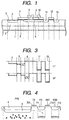
- Fig. 1 is a schematic cross-sectional view of a common CCD
- Fig. 2 shows the change of the potential distribution in time of various areas shown in Fig. 1, wherein areas same as those in Fig. 1 are represented by same numbers.
- a Si semiconductor substrate 1 of a first conductive type a well area 2 of a second conductive type opposite to that of the substrate 1, and a diffusion area 3 of the first conductive type, constituting a PN photodiode with the well area 2.
- the PN photodiode is initially given an inverse bias and a photo-induced charge is accumulated according to the incident light amount, in the junction capacitance of the PN photodiode.
- a shallow diffusion area 4 of the second conductive type provided for reducing the dark current generated on the surface of the diffusion area 3 and forming a diode also between the areas 3 and 4 thereby increasing the amount of the accumulated charge
- a transfer channel 5 for reading the photo-induced charge accumulated in the photodiode
- a CCD channel 6 for successive transfer of the read charge.
- a control electrode 7 serves to control the charge transfer to the CCD and also the successive charge transfer in the CCD, and is formed on the transfer channel 5 and the CCD channel 6 across an insulation layer.
- Second, third and fourth electrodes 8, 9, 10 serve to transfer the charge in the CCD in succession.
- a floating diffusion area 11 finally receives the transferred photo-induced charge, and a voltage amplitude, generated in the floating diffusion area 11 according to the photo-induced charge amount, is detected by a source follower amplifier, omitted in Fig. 1, and outputted to the outside as an electrical signal.
- a reset gate 12 for resetting the floating diffusion area 11, and a reset drain 13 therefor.
- Fig. 2 illustrates the potential states of the various areas.
- the transfer channel 5 is turned off and the photodiode area 2, 3 accumulates the photo-induced charge corresponding to the incident light amount.
- the transfer channel is turned on to transfer the photo-induced charge to the CCD channel 6 through the transfer channel 5.
- the control electrodes 8, 9 are controlled in succession to transfer the photo-induced charge is transferred in succession to the portions in the CCD channel, positioned directly below the control electrodes.
- the floating diffusion area 11 is reset in advance at the time t3, and, the photo-induced charge is transferred by the control electrode 10, at a time t4, to the floating diffusion area 11 and is converted therein into a voltage for output.
- the common control electrode 7 is used for controlling the potentials of the transfer channel 5 and the first CCD channel 6, the difference in the depth of the potential wells thereof is uniquely determined by the process conditions such as the concentration profile. For this reason, there may result a case where the depth of the potential well of the CCD channel 6 cannot be sufficiently secured as shown in Fig. 3 in which areas same as those in Fig. 1 are represented by same numbers. As a result, the photo-induced charge cannot be fully transferred but partly remains in the transfer channel 5, leading to defective phenomena such as:
- Japanese Patent Application Laid-open No. 2-30189 discloses a configuration having an electrode for controlling the charge transfer from the photodiode to the CCD channel and another electrode for controlling the charge transfer in the CCD, as shown in Fig. 5.
- a plurality of n-type accumulation areas 1 for accumulating the signal charges induced by the incident light are arranged on a p-type substrate 6, and a transfer gate 13 is provided between the accumulation area 1 and a vertical CCD register 2, of which an end is connected to a horizontal CCD register composed of a transfer gate 12, a transfer electrode 13 for the vertical CCD register and a silicon dioxide layer 14.
- VA denotes the potential of the n-type accumulation area 1, taking the Fermi potential 15 of the interior of the p-type substrate as a reference, while VDEP denotes the potential VA required for completely depleting the accumulation area 1, and Vch denotes the channel potential when the transfer gate 3 is turned on.
- the potential VA is lowered in the drawing in response to the light entering the accumulation area 1, and the accumulated charge is transferred to the vertical CCD register 2 by lowering the potential of the gate 12.
- the depth of the potential well of the CCD channel is still uniquely determined by the process conditions such as the concentration profile, so that there are similarly encountered the above-mentioned drawbacks.
- CMOS/CCD Process Technology exhibited at 95 IEEE WORKSHOP on Charge-coupled Device and Advanced Image Sensors
- Fig. 4 discloses a CMOS sensor and its potential chart as shown in Fig. 4.
- Fig. 4 in the CMOS sensor, the floating diffusion area and the source follower amplifier are provided for each pixel, instead of at the end of the CCD register in case of the CCD.
- components same as those in Fig. 1 are represented by same numbers.
- a transfer gate 701 provided for each pixel, and a floating diffusion area 711 provided for each pixel.
- the photo-induced charge, generated in the photodiode area is transferred to the floating diffusion area 711, and the amplitude of the voltage generated therein according to amount of photo-induced charges is detected by the source follower amplifier, omitted in Fig. 4 but provided for each pixel, and outputted to an output line through a pixel selecting switch.
- Such circuit configuration of transferring the charge of each pixel to the corresponding floating diffusion area 711 and effecting the selection of pixels by a common MOS circuit allows achieve both a high S/N ratio as the sensor and a high performance realized by a one-chip MOS circuit.
- the object of the present invention is to provide a configuration of the solid state image pickup apparatus, capable of complete transfer of the charge from the photoelectric conversion element to the floating diffusion area.
- a solid state image pickup apparatus comprising a photoelectric conversion element, transfer switch means consisting of a MOS transistor for transferring a signal charge generated in the photoelectric conversion element, a floating diffusion capacitance for receiving the signal charge through the transfer switch means, and reset switch means consisting of a MOS transistor for resetting the potential of the floating diffusion capacitance
- the pickup apparatus further comprises at least one potential setting means for generating a voltage different from the power supply voltage, and the output of the potential setting means is supplied as a pulse to the gate of the transfer switch means and/or the gate of the reset switch means, to control the gate potentials at the respectively optimum potentials.
- a solid state image pickup apparatus comprising a PN junction unit capable of photoelectric conversion, a transferring MOS transistor for transferring a signal charge generated in the PN junction unit, a floating diffusion unit for receiving the signal charge through the transferring MOS transistor, a reset MOS transistor for resetting the potential of the floating diffusion unit, first potential setting means for supplying a voltage to be applied to the gate of the transferring MOS transistor and a second potential setting means for supplying a voltage to be applied to the resetting MOS transistor.
- Fig. 6A is a schematic view showing the first embodiment of the present invention, wherein shown are a Si semiconductor substrate 1 of a first conductive type, a well area of a second conductive type opposite to that of the substrate 1, a diffusion area 3 of the first conductive type, forming a PN photodiode with the well area 2, a shallow diffusion area 4 of the second conductive type, a transfer channel 5 for reading the photo-induced charge accumulated in the photodiode, a floating diffusion area 11, a reset gate 12 for resetting the floating diffusion area 11, and a reset drain 13 therefor.
- Components same as those in Fig. 5 are represented by same numbers and will not be explained further.
- a transfer gate 501 of a transfer switch for transferring the photo-induced charge in the photodiode 2, 3, 4, a control pulse generation circuit 504, a first potential setting circuit 502 for setting the voltage of the control signal generated by the control pulse generation circuit 504 for application to the transfer gate 501, and a second potential setting circuit 503 for setting the voltage of the control signal generated by the control pulse generation circuit 504 to supply that voltage to the reset gate 12.
- the first and second potential setting circuits 502, 503 are so constructed that the transfer gate 501 and the reset gate 12 can be set at respectively independent potentials.
- Fig. 6B showing the potential state of various areas at different timings.
- the transfer channel 5 is turned off and a photo-induced charge is accumulated in the photodiode area 2 - 4 according to the amount of the incident light.
- the floating diffusion area 11 is reset by turning on the reset gate at a time t1.
- the photo-induced charge is transferred from the photodiode area 2 - 4 through the transfer channel 5 to the floating diffusion area 11 and converted therein into a voltage and outputted.
- the transfer channel 5 is turned off again, and the photodiode area 2 - 4 of each pixel starts next charge accumulation.
- the charge may remain in the transfer channel 5 because of a fluctuation in the resetting voltage, resulting for example from a fluctuation in the manufacturing process.
- a power supply line is commonly used for resetting and for the source follower circuit of each pixel, in order to simplify the wiring and to achieve a compacter layout, thereby reducing the pixel size and increasing the aperture ratio.
- the resetting voltage is selected not as the actual power source voltage but as a value determined by the threshold value Vth of the resetting MOS transistor.
- a photodiode 101 accumulates a photo-induced charge which is transferred by a transfer switch 102, and the transferred photo-induced charge is temporarily stored in a floating diffusion area 103, amplified by a source follower MOS transistor 104 and is read out by a vertical selecting MOS transistor 105 to an output line 106.
- the floating diffusion area is connected to a power source through a resetting MOS transistor 107, and, in the resetting operation by the application of a voltage of 5 V to the gate thereof, the floating diffusion area is reset to a potential of 5 V - Vth.
- the resetting voltage becomes 5 V - Vth.
- the threshold voltage of the MOS transistor cannot be made completely free from fluctuation because of fluctuation in the fluctuation of the Si layer or in the thickness of the gate insulation layer, so that the resetting voltage inevitably shows a fluctuation.
- the effective resetting voltage is lowered so that the potential well becomes shallower as shown in t2' in Fig. 7A.
- the gate voltage and the threshold voltage of the transferring MOS transistor remain constant, there will result charge remaining in the channel of the transferring MOS transistor as shown in t2'.
- the voltage of the gate 501 of the transferring MOS transistor is lowered to reduce the potential of the channel 5 thereof, thereby transferring the charge in the channel to the floating diffusion area.
- the gate-on voltage Vg of the transferring MOS transistor is so set as to satisfy a relation 1 + Vth' ⁇ Vg ⁇ 2 + Vth' (for example 2.5 V ⁇ Vg ⁇ 3.5 V).
- Vg is selected as 3.3 V.
- the saturation voltage at the floating diffusion area becomes 1.7 V, so that the charge remains in the channel of the transferring MOS transistor unless Vg is so selected as to satisfy a condition 2.5 V ⁇ Vg ⁇ 3.2 V.
- the proper operation without the retentive charge can be achieved by changing Vg from 3.3 V to for example 3.0 V so as to satisfy the above-mentioned condition.
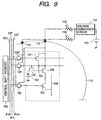
- Fig. 9 shows a solid state image pickup apparatus 110 for converting incident light into an electrical signal for output to the exterior and a voltage supply unit for driving the solid state image pickup apparatus 110, both apparatus and unit being formed on a same semiconductor chip.
- Fig. 9 the circuit in a broken-lined frame is same as that shown in Fig. 8.
- Fig. 9 there are shown a vertical shift register 108 for outputting pulses in succession, and AND circuits 109, 109' and 109'' each having two input/output terminals and an electric power source terminal for driving the AND circuit.
- this AND circuit once high voltage is applied to both two input terminals, a voltage value of the electric power source voltage for driving of the AND circuit is output from the output terminal.
- an AND circuit having a CMOS structure may be available, for example.
- a voltage supply unit 113 such as a battery
- a voltage conversion circuit 114 for converting the voltage of the voltage supply unit 114 into a desired voltage
- variable resistors 115, 116 for entering a voltage for driving the solid state image pickup apparatus
- an input terminal 111 for entering a voltage for driving the transferring MOS transistor.
- signal lines 105', 102' and 107' for respectively supplying pulses ⁇ SEL , ⁇ TX and ⁇ RES to be used to turn on and off the vertical selecting MOS transistor 105, the transfer switch 102 and the resetting MOS transistor 107.
- the AND circuit 109 Under a condition that a pulse is applied from the vertical shift register to one of input terminals of each of the three AND circuits, the AND circuit 109 outputs the voltage value input from the terminal 112, when the pulse ⁇ SEL is applied to the signal line 105'; the AND circuit 109' outputs the voltage value input from the terminal 111, when the pulse ⁇ TX is applied to the signal line 102'; and the AND circuit 109'' outputs the voltage value input from the terminal 112, when the pulse ⁇ RES is applied to the signal line 107'.
- the AND circuit 109, the input terminal 111 and the variable resistor 116 constitute the first voltage setting circuit 502 shown in Figs. 6A and 6B.
- the potential well can be realized in a form as shown by t2'' in Fig. 7A by reducing the voltage entered from the input terminal 111.
- the pulse voltage for driving the transferring MOS transistor can be adjusted independently from the pulse voltage for driving the resetting MOS transistor. Consequently, even if the resetting voltage is lowered by the fluctuation in the manufacturing process, the ideal potential well can be formed by adjusting the pulse for driving the transferring MOS transistor.
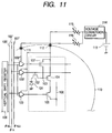
- Fig. 10 is a view showing the potentials of various areas for explaining a second embodiment of the present invention.
- the present embodiment is to achieve a similar effect by controlling the voltage of the resetting MOS transistor.
- the circuit configuration corresponding to Fig. 10 is similar to that shown in Figs. 6A and 6B and will not, therefore, be explained further.
- the circuit shown in Fig. 11 is different from that shown in Fig. 9 in that the voltage entered from the input terminal 111 is supplied to the gate of the resetting MOS transistor 107 and the voltage entered from the power supply voltage input terminal 112 is supplied to the gate of the transferring MOS transistor 102.
- the AND circuit 109, the input terminal 111 and the variable resistor 116 constitute the second potential setting circuit 503 shown in Figs. 6A and 6B.
- the potential well can be realized in a form as shown by t2'' in Fig. 10 by elevating the voltage entered from the input terminal 111.
- the pulse voltage for driving the resetting MOS transistor can be adjusted independently from the pulse voltage for driving the transferring MOS transistor. Consequently, even if the potential of the floating diffusion area comes close to that of the transferring MOS transistor by the fluctuation in the manufacturing process, the ideal potential well can be formed by adjusting the pulse for driving the resetting MOS transistor.
- the state at a time t2 in Fig. 10 is same as that at a time t2 in Fig. 6B. Also in the present embodiment, the operations at the time t0 and t1 are same as those in Fig. 6B.
- the resetting voltage may vary for example because of fluctuation in the manufacturing process, resulting in a charge remaining in the transfer channel 5.
- the voltage of the reset gate 12 is independently controlled by the second potential setting circuit 503 for elevating the resetting voltage of the floating diffusion area 11. For example, if the resetting voltage varies from 3.5 V to 3.3 V in the example shown in Fig. 7B, it can be returned to 3.5 V by varying the gate-on voltage of the resetting MOS transistor. In this manner, the proper transferring operation can be realized without changing the conditions of the transferring MOS transistor.
- Such setting realizes a condition: saturation voltage of floating diffusion area 11 > channel voltage of transfer MOS transistor in on-state > depletion voltage of photodiode, whereby the charge can be transferred to the floating diffusion area without remaining on the photodiode and the channel of the transferring MOS transistor, and there can be achieved an effect similar to that of the first embodiment for preventing the charge remaining in the transfer channel 5.
- the AND circuit 109, the input terminal 111 and the variable resistor 116 constitute a first potential setting circuit, while the AND circuit 109, the input terminal 111' and the variable resistor 116' constitute a second potential setting circuit.
- the first and second potential setting circuits may be provided, as shown in Fig. 13, in a same semiconductor chip in which the solid state image pickup circuit is formed.
- the solid state image pickup apparatus may include a voltage adjusting circuit 117 capable of supplying different voltages, for adjusting the voltages supplied to the transferring MOS transistor and the resetting MOS transistor.
- the circuit shown in Fig. 13 is so designed as to independently set the power supply voltage for driving the solid state image pickup apparatus, the voltage supplied to the gate of the transferring MOS transistor and the voltage supplied to the gate of the resetting MOS transistor, but the voltage supplied to the gate of the transferring MOS transistor or that supplied to the gate of the resetting MOS transistor may be made common with the power supply voltage.
- the first and second potential setting circuits are constituted by the AND circuit 109 and a voltage adjusting circuit.
- the present invention allows to avoid remaining of the photo-induced charge in the transfer channel even in the presence of fluctuation of the manufacturing process, thereby providing advantages such as:
Abstract
Description
- The present invention relates to a solid state image pickup apparatus, and more particularly to a solid state image pickup apparatus having a floating diffusion unit adjacent to the photoelectric conversion unit.
- Conventionally, the charge coupled device (CCD) is widely utilized as the solid state image pickup apparatus. Fig. 1 is a schematic cross-sectional view of a common CCD, and Fig. 2 shows the change of the potential distribution in time of various areas shown in Fig. 1, wherein areas same as those in Fig. 1 are represented by same numbers.
- In Fig. 1 there are shown a
Si semiconductor substrate 1 of a first conductive type, awell area 2 of a second conductive type opposite to that of thesubstrate 1, and adiffusion area 3 of the first conductive type, constituting a PN photodiode with thewell area 2. The PN photodiode is initially given an inverse bias and a photo-induced charge is accumulated according to the incident light amount, in the junction capacitance of the PN photodiode. There are also shown ashallow diffusion area 4 of the second conductive type, provided for reducing the dark current generated on the surface of thediffusion area 3 and forming a diode also between theareas transfer channel 5 for reading the photo-induced charge accumulated in the photodiode, and aCCD channel 6 for successive transfer of the read charge. - A control electrode 7 serves to control the charge transfer to the CCD and also the successive charge transfer in the CCD, and is formed on the
transfer channel 5 and theCCD channel 6 across an insulation layer. Second, third andfourth electrodes floating diffusion area 11 finally receives the transferred photo-induced charge, and a voltage amplitude, generated in thefloating diffusion area 11 according to the photo-induced charge amount, is detected by a source follower amplifier, omitted in Fig. 1, and outputted to the outside as an electrical signal. There are also shown areset gate 12 for resetting thefloating diffusion area 11, and areset drain 13 therefor. - In the following the functions will be explained with reference to Fig. 2, which illustrates the potential states of the various areas. At a time t0, the
transfer channel 5 is turned off and thephotodiode area CCD channel 6 through thetransfer channel 5. - At times t2, t3, the
control electrodes floating diffusion area 11 is reset in advance at the time t3, and, the photo-induced charge is transferred by thecontrol electrode 10, at a time t4, to thefloating diffusion area 11 and is converted therein into a voltage for output. - In the above-described configuration, however, as the common control electrode 7 is used for controlling the potentials of the
transfer channel 5 and thefirst CCD channel 6, the difference in the depth of the potential wells thereof is uniquely determined by the process conditions such as the concentration profile. For this reason, there may result a case where the depth of the potential well of theCCD channel 6 cannot be sufficiently secured as shown in Fig. 3 in which areas same as those in Fig. 1 are represented by same numbers. As a result, the photo-induced charge cannot be fully transferred but partly remains in thetransfer channel 5, leading to defective phenomena such as: - (1) a decrease in the total amount of the transferred charge, leading to a lowered sensitivity; and
- (2) return of the charge remaining in the
transfer channel 5 to thephotodiode -
- Also the Japanese Patent Application Laid-open No. 2-30189 discloses a configuration having an electrode for controlling the charge transfer from the photodiode to the CCD channel and another electrode for controlling the charge transfer in the CCD, as shown in Fig. 5. Referring to Fig. 5, a plurality of n-
type accumulation areas 1 for accumulating the signal charges induced by the incident light are arranged on a p-type substrate 6, and atransfer gate 13 is provided between theaccumulation area 1 and avertical CCD register 2, of which an end is connected to a horizontal CCD register composed of atransfer gate 12, atransfer electrode 13 for the vertical CCD register and asilicon dioxide layer 14. VA denotes the potential of the n-type accumulation area 1, taking the Fermipotential 15 of the interior of the p-type substrate as a reference, while VDEP denotes the potential VA required for completely depleting theaccumulation area 1, and Vch denotes the channel potential when thetransfer gate 3 is turned on. The potential VA is lowered in the drawing in response to the light entering theaccumulation area 1, and the accumulated charge is transferred to thevertical CCD register 2 by lowering the potential of thegate 12. - However, according to the above-mentioned patent application, the depth of the potential well of the CCD channel is still uniquely determined by the process conditions such as the concentration profile, so that there are similarly encountered the above-mentioned drawbacks.
- In the field of solid state image pickup apparatus, in addition to CCD, the MOS sensor is recently attracting attention and is actively developed because of the advantages such as ease of one-chip formation of the peripheral circuits. For example, an exhibit titled "An Active Pixel Sensor Fabricated Ysing CMOS/CCD Process Technology" (exhibited at 95 IEEE WORKSHOP on Charge-coupled Device and Advanced Image Sensors) discloses a CMOS sensor and its potential chart as shown in Fig. 4. As shown in Fig. 4, in the CMOS sensor, the floating diffusion area and the source follower amplifier are provided for each pixel, instead of at the end of the CCD register in case of the CCD. In Fig. 4, components same as those in Fig. 1 are represented by same numbers. There are also shown a transfer gate 701 provided for each pixel, and a floating diffusion area 711 provided for each pixel. The photo-induced charge, generated in the photodiode area is transferred to the floating diffusion area 711, and the amplitude of the voltage generated therein according to amount of photo-induced charges is detected by the source follower amplifier, omitted in Fig. 4 but provided for each pixel, and outputted to an output line through a pixel selecting switch. There are also shown a
reset gate 712 for resetting the floating diffusion area 711 provided for each pixel, and areset drain 713 therefor. - Such circuit configuration of transferring the charge of each pixel to the corresponding floating diffusion area 711 and effecting the selection of pixels by a common MOS circuit allows achieve both a high S/N ratio as the sensor and a high performance realized by a one-chip MOS circuit.
- However, such conventional configuration is still associated with the drawbacks similar to those in the conventional CCD configuration, because of changes in the reset voltage in the floating diffusion area and in the depth of the potential well of the transfer channel, caused by a fluctuation in the manufacturing process conditions. These drawbacks have not been paid any attention, and the potential chart of the aforementioned exhibit only showed a configuration that is incapable of complete transfer of the charge from the photodiode to the floating diffusion area.
- The object of the present invention is to provide a configuration of the solid state image pickup apparatus, capable of complete transfer of the charge from the photoelectric conversion element to the floating diffusion area.
- The above-mentioned object can be attained, according to a scope of the present invention, by providing a solid state image pickup apparatus comprising a photoelectric conversion element, transfer switch means consisting of a MOS transistor for transferring a signal charge generated in the photoelectric conversion element, a floating diffusion capacitance for receiving the signal charge through the transfer switch means, and reset switch means consisting of a MOS transistor for resetting the potential of the floating diffusion capacitance, wherein the pickup apparatus further comprises at least one potential setting means for generating a voltage different from the power supply voltage, and the output of the potential setting means is supplied as a pulse to the gate of the transfer switch means and/or the gate of the reset switch means, to control the gate potentials at the respectively optimum potentials.
- According to an another aspect of the present invention, there is provided a solid state image pickup apparatus comprising a PN junction unit capable of photoelectric conversion, a transferring MOS transistor for transferring a signal charge generated in the PN junction unit, a floating diffusion unit for receiving the signal charge through the transferring MOS transistor, a reset MOS transistor for resetting the potential of the floating diffusion unit, first potential setting means for supplying a voltage to be applied to the gate of the transferring MOS transistor and a second potential setting means for supplying a voltage to be applied to the resetting MOS transistor.
- These configurations allows to obtain a satisfactory image.
- Other objects of the present invention, and the features thereof, will become fully apparent from the following description, which is to be taken in conjunction with the attached drawings.
-
- Fig. 1 is a schematic cross-sectional view of a conventional CCD;
- Fig. 2 is a chart showing the function of the conventional configuration;
- Fig. 3 is a view showing a drawback in the conventional configuration;
- Fig. 4 is a schematic cross-sectional view of a second configuration;
- Fig. 5 is a view schematically showing first and second embodiments of the present invention and the function thereof;
- Figs. 6A, 6B, 7A, 7B, 8 and 9 are views showing the function of the first embodiment of the present invention;
- Figs. 10 and 11 are views showing the function of the second embodiment of the present invention; and
- Figs. 12 and 13 are views showing the function of the first and second embodiments of the present invention.
-
- Now there will be given a detailed description on a first embodiment of the present invention, with reference to the attached drawings. Fig. 6A is a schematic view showing the first embodiment of the present invention, wherein shown are a
Si semiconductor substrate 1 of a first conductive type, a well area of a second conductive type opposite to that of thesubstrate 1, adiffusion area 3 of the first conductive type, forming a PN photodiode with thewell area 2, ashallow diffusion area 4 of the second conductive type, atransfer channel 5 for reading the photo-induced charge accumulated in the photodiode, afloating diffusion area 11, areset gate 12 for resetting thefloating diffusion area 11, and areset drain 13 therefor. Components same as those in Fig. 5 are represented by same numbers and will not be explained further. - There are also provided a
transfer gate 501 of a transfer switch for transferring the photo-induced charge in thephotodiode pulse generation circuit 504, a firstpotential setting circuit 502 for setting the voltage of the control signal generated by the controlpulse generation circuit 504 for application to thetransfer gate 501, and a secondpotential setting circuit 503 for setting the voltage of the control signal generated by the controlpulse generation circuit 504 to supply that voltage to thereset gate 12. - The first and second
potential setting circuits transfer gate 501 and thereset gate 12 can be set at respectively independent potentials. - Now, the function of the present embodiment will be explained with reference to Fig. 6B showing the potential state of various areas at different timings. At a time t0, the
transfer channel 5 is turned off and a photo-induced charge is accumulated in the photodiode area 2 - 4 according to the amount of the incident light. Thefloating diffusion area 11 is reset by turning on the reset gate at a time t1. Then, at a time t2, the photo-induced charge is transferred from the photodiode area 2 - 4 through thetransfer channel 5 to thefloating diffusion area 11 and converted therein into a voltage and outputted. At a time t3, thetransfer channel 5 is turned off again, and the photodiode area 2 - 4 of each pixel starts next charge accumulation. - In these operations, as shown at time t2' in Fig. 7A, the charge may remain in the
transfer channel 5 because of a fluctuation in the resetting voltage, resulting for example from a fluctuation in the manufacturing process. Ordinarily, a power supply line is commonly used for resetting and for the source follower circuit of each pixel, in order to simplify the wiring and to achieve a compacter layout, thereby reducing the pixel size and increasing the aperture ratio. Such configuration is adopted also in the present embodiment, and the resetting voltage is selected not as the actual power source voltage but as a value determined by the threshold value Vth of the resetting MOS transistor. - For explaining the circuit configuration of the solid state image pickup apparatus, an equivalent circuit corresponding to a pixel is shown in Fig. 8. A
photodiode 101 accumulates a photo-induced charge which is transferred by atransfer switch 102, and the transferred photo-induced charge is temporarily stored in a floatingdiffusion area 103, amplified by a sourcefollower MOS transistor 104 and is read out by a vertical selectingMOS transistor 105 to anoutput line 106. The floating diffusion area is connected to a power source through a resettingMOS transistor 107, and, in the resetting operation by the application of a voltage of 5 V to the gate thereof, the floating diffusion area is reset to a potential of 5 V - Vth. - For example, if the gate voltage of the resetting MOS transistor is 5 V for a power source voltage of 5 V, the resetting voltage becomes 5 V - Vth. The threshold voltage of the MOS transistor cannot be made completely free from fluctuation because of fluctuation in the fluctuation of the Si layer or in the thickness of the gate insulation layer, so that the resetting voltage inevitably shows a fluctuation.
- Also with an increase in the threshold value Vth, the effective resetting voltage is lowered so that the potential well becomes shallower as shown in t2' in Fig. 7A. In such state, if the gate voltage and the threshold voltage of the transferring MOS transistor remain constant, there will result charge remaining in the channel of the transferring MOS transistor as shown in t2'. In order to prevent such charge remaining phenomenon, it is effective to lower the gate voltage of the transferring MOS transistor as shown in t2''. Consequently the voltage of the
gate 501 of the transferring MOS transistor is controlled by the firstpotential setting circuit 502, independently from the voltage of thegate 12 of the resetting MOS transistor. Also in order to shift from the state shown in t2' in Fig. 7A to the state shown in t2'', the voltage of thegate 501 of the transferring MOS transistor is lowered to reduce the potential of thechannel 5 thereof, thereby transferring the charge in the channel to the floating diffusion area. - More specifically, in case of the electron accumulation type as shown in Fig. 7B, for example when a gate-on voltage is 5 V for the resetting MOS transistor, a reset voltage is 3.5 V = 5 V - Vth (Vth = 1.5 V) for the floating diffusion area, a saturation signal voltage is 1.5 V, a saturation voltage is 2 V for the floating diffusion area and a depletion voltage is 1 V for the photodiode, the gate-on voltage Vg of the transferring MOS transistor is so set as to satisfy a
relation - If the resetting voltage varies from 3.5 V to 3.2 V by the fluctuation of the process, the saturation voltage at the floating diffusion area becomes 1.7 V, so that the charge remains in the channel of the transferring MOS transistor unless Vg is so selected as to satisfy a condition 2.5 V < Vg < 3.2 V.
- In such case, the proper operation without the retentive charge can be achieved by changing Vg from 3.3 V to for example 3.0 V so as to satisfy the above-mentioned condition.
- Now there will be given, with reference to Fig. 9, a detailed explanation on the first potential setting circuit shown in Figs. 6A and 6B.
- Fig. 9 shows a solid state
image pickup apparatus 110 for converting incident light into an electrical signal for output to the exterior and a voltage supply unit for driving the solid stateimage pickup apparatus 110, both apparatus and unit being formed on a same semiconductor chip. - In the solid state
image pickup apparatus 110, there is only shown a pixel, while other pixels, horizontal shift register etc. are omitted. - In Fig. 9, the circuit in a broken-lined frame is same as that shown in Fig. 8. In Fig. 9, there are shown a
vertical shift register 108 for outputting pulses in succession, and ANDcircuits 109, 109' and 109'' each having two input/output terminals and an electric power source terminal for driving the AND circuit. In this AND circuit, once high voltage is applied to both two input terminals, a voltage value of the electric power source voltage for driving of the AND circuit is output from the output terminal. As this AND circuit, an AND circuit having a CMOS structure may be available, for example. - There are also shown a
voltage supply unit 113 such as a battery, avoltage conversion circuit 114 for converting the voltage of thevoltage supply unit 114 into a desired voltage,variable resistors voltage input terminal 112 for entering a voltage for driving the solid state image pickup apparatus, and aninput terminal 111 for entering a voltage for driving the transferring MOS transistor. In addition, there are shown signal lines 105', 102' and 107' for respectively supplying pulses SEL, TX and RES to be used to turn on and off the vertical selectingMOS transistor 105, thetransfer switch 102 and the resettingMOS transistor 107. Under a condition that a pulse is applied from the vertical shift register to one of input terminals of each of the three AND circuits, the ANDcircuit 109 outputs the voltage value input from the terminal 112, when the pulse SEL is applied to the signal line 105'; the AND circuit 109' outputs the voltage value input from the terminal 111, when the pulse TX is applied to the signal line 102'; and the AND circuit 109'' outputs the voltage value input from the terminal 112, when the pulse RES is applied to the signal line 107'. In the present embodiment, the ANDcircuit 109, theinput terminal 111 and thevariable resistor 116 constitute the firstvoltage setting circuit 502 shown in Figs. 6A and 6B. - Thus, even if the threshold voltage Vth of the resetting
MOS transistor 107 increases to reduce the effective resetting voltage whereby the potential well becomes shallow as shown by t2' in Fig. 7A, the above-described configuration can solve the situation in the following manner. - As the voltage entered from the
input terminal 111 can be made different, by the variable resistor, from the voltage entered from the power supplyvoltage input terminal 112, the potential well can be realized in a form as shown by t2'' in Fig. 7A by reducing the voltage entered from theinput terminal 111. Thus, in the present embodiment, the pulse voltage for driving the transferring MOS transistor can be adjusted independently from the pulse voltage for driving the resetting MOS transistor. Consequently, even if the resetting voltage is lowered by the fluctuation in the manufacturing process, the ideal potential well can be formed by adjusting the pulse for driving the transferring MOS transistor. - Such operation prevents the presence of the photo-induced charge remaining in the
transfer channel 5, thereby providing advantages such as: - a) securing a constant amount of the total transferred charge, thereby ensuring a constant sensitivity; and
- b) avoiding generation of the retentive image.
-
- Fig. 10 is a view showing the potentials of various areas for explaining a second embodiment of the present invention. In contrast to the first embodiment in which the proper transferring operation is realized, even in the presence of fluctuation in the manufacturing process, by controlling the voltage of the transferring MOS transistor, the present embodiment is to achieve a similar effect by controlling the voltage of the resetting MOS transistor. The circuit configuration corresponding to Fig. 10 is similar to that shown in Figs. 6A and 6B and will not, therefore, be explained further.
- In the following there will be explained, with reference to Fig. 11, the second setting circuit shown in Figs. 6A and 6B.
- The circuit shown in Fig. 11 is different from that shown in Fig. 9 in that the voltage entered from the
input terminal 111 is supplied to the gate of the resettingMOS transistor 107 and the voltage entered from the power supplyvoltage input terminal 112 is supplied to the gate of the transferringMOS transistor 102. In the present embodiment, the ANDcircuit 109, theinput terminal 111 and thevariable resistor 116 constitute the secondpotential setting circuit 503 shown in Figs. 6A and 6B. - Thus, even if the threshold voltage Vth of the resetting
MOS transistor 107 increases to reduce the effective resetting voltage whereby the potential well becomes shallow as shown by t2' in Fig. 10, the above-described configuration can solve the situation in the following manner. - As the voltage entered from the
input terminal 111 can be made different, by the variable resistor, from the voltage entered from the power supplyvoltage input terminal 112, the potential well can be realized in a form as shown by t2'' in Fig. 10 by elevating the voltage entered from theinput terminal 111. Thus, in the present embodiment, the pulse voltage for driving the resetting MOS transistor can be adjusted independently from the pulse voltage for driving the transferring MOS transistor. Consequently, even if the potential of the floating diffusion area comes close to that of the transferring MOS transistor by the fluctuation in the manufacturing process, the ideal potential well can be formed by adjusting the pulse for driving the resetting MOS transistor. - The state at a time t2 in Fig. 10 is same as that at a time t2 in Fig. 6B. Also in the present embodiment, the operations at the time t0 and t1 are same as those in Fig. 6B.
- As shown at a time t2' in Fig. 10, the resetting voltage may vary for example because of fluctuation in the manufacturing process, resulting in a charge remaining in the
transfer channel 5. In the present embodiment, however, the voltage of thereset gate 12 is independently controlled by the secondpotential setting circuit 503 for elevating the resetting voltage of the floatingdiffusion area 11. For example, if the resetting voltage varies from 3.5 V to 3.3 V in the example shown in Fig. 7B, it can be returned to 3.5 V by varying the gate-on voltage of the resetting MOS transistor. In this manner, the proper transferring operation can be realized without changing the conditions of the transferring MOS transistor. Such setting realizes a condition:
saturation voltage of floatingdiffusion area 11 > channel voltage of transfer MOS transistor in on-state > depletion voltage of photodiode,
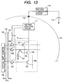
whereby the charge can be transferred to the floating diffusion area without remaining on the photodiode and the channel of the transferring MOS transistor, and there can be achieved an effect similar to that of the first embodiment for preventing the charge remaining in thetransfer channel 5. - In the foregoings, there have been explained configurations provided with the separate first or second potential setting circuit as shown in Figs. 9 and 11, but the solid state image pickup apparatus may be integrally provided with the first and second potential setting circuits as shown in Fig. 12.
- In Fig. 12, the AND
circuit 109, theinput terminal 111 and thevariable resistor 116 constitute a first potential setting circuit, while the ANDcircuit 109, the input terminal 111' and the variable resistor 116' constitute a second potential setting circuit. - Also the first and second potential setting circuits may be provided, as shown in Fig. 13, in a same semiconductor chip in which the solid state image pickup circuit is formed. Stated differently, the solid state image pickup apparatus may include a
voltage adjusting circuit 117 capable of supplying different voltages, for adjusting the voltages supplied to the transferring MOS transistor and the resetting MOS transistor. - The circuit shown in Fig. 13 is so designed as to independently set the power supply voltage for driving the solid state image pickup apparatus, the voltage supplied to the gate of the transferring MOS transistor and the voltage supplied to the gate of the resetting MOS transistor, but the voltage supplied to the gate of the transferring MOS transistor or that supplied to the gate of the resetting MOS transistor may be made common with the power supply voltage. In Fig. 13, the first and second potential setting circuits are constituted by the AND
circuit 109 and a voltage adjusting circuit. - As explained in the foregoing first and second embodiments, the present invention allows to avoid remaining of the photo-induced charge in the transfer channel even in the presence of fluctuation of the manufacturing process, thereby providing advantages such as:
- a) securing a constant amount of the total transferred charge, thus maintaining a constant sensitivity; and
- b) preventing generation of the retentive image.
-
- Many widely different embodiments of the present invention may be constructed without departing from the spirit and scope of the present invention. It should be understood that the present invention is not limited to the specific embodiments described in the specification, except as defined in the appended claims.
Claims (5)
- A solid state image pickup apparatus comprising a photoelectric conversion element, transfer switch means consisting of a MOS transistor for transferring a signal charge generated in said photoelectric conversion element, a floating diffusion area for receiving the signal charge through said transfer switch means, and reset switch means consisting of a MOS transistor for resetting the potential of said floating diffusion area, and at least one potential setting means for generating a voltage different from the power supply voltage, wherein the output of said potential setting means is applied as a pulse to the gate of said transfer switch means and/or the gate of said reset switch means.
- A solid state image pickup apparatus according to claim 1, wherein the amplitude of the pulse applied to the gate of said transfer switch means is different from that of the pulse applied to the gate of the reset switch means.
- A solid state image pickup apparatus according to claim 1 or 2, wherein the amplitude of the pulse applied to the gate of said transfer switch means is smaller than that of the pulse applied to the gate of the reset switch means.
- A solid state image pickup apparatus according to claim 1 or 2, wherein said photoelectric conversion element is a PN photodiode formed on a semiconductor substrate.
- A solid state image pickup apparatus comprising a PN junction capable of photoelectric conversion, a transferring MOS transistor for transferring a signal charge generated in said PN junction, a floating diffusion area for receiving the signal charge through said transferring MOS transistor, and a resetting MOS transistor for resetting the potential of said floating diffusion area, characterized infirst potential setting means for setting the voltage applied to the gate of said transferring MOS transistor; andsecond potential setting means for setting the voltage applied to the gate of said setting MOS transistor.
Applications Claiming Priority (2)
| Application Number | Priority Date | Filing Date | Title |
|---|---|---|---|
| JP10061231A JPH11261046A (en) | 1998-03-12 | 1998-03-12 | Solid-state image pickup device |
| JP06123198 | 1998-03-12 |
Publications (3)
| Publication Number | Publication Date |
|---|---|
| EP0942593A2 true EP0942593A2 (en) | 1999-09-15 |
| EP0942593A3 EP0942593A3 (en) | 2000-09-06 |
| EP0942593B1 EP0942593B1 (en) | 2008-01-16 |
Family
ID=13165252
Family Applications (1)
| Application Number | Title | Priority Date | Filing Date |
|---|---|---|---|
| EP99301832A Expired - Lifetime EP0942593B1 (en) | 1998-03-12 | 1999-03-11 | Solid state image pickup apparatus |
Country Status (4)
| Country | Link |
|---|---|
| US (1) | US7110030B1 (en) |
| EP (1) | EP0942593B1 (en) |
| JP (1) | JPH11261046A (en) |
| DE (1) | DE69937978D1 (en) |
Cited By (5)
| Publication number | Priority date | Publication date | Assignee | Title |
|---|---|---|---|---|
| EP1143708A1 (en) | 2000-02-28 | 2001-10-10 | Canon Kabushiki Kaisha | Image pickup apparatus |
| US6528833B2 (en) * | 2000-06-20 | 2003-03-04 | Pixelplus Co., Ltd. | CMOS active pixel for improving sensitivity |
| FR2857158A1 (en) * | 2003-07-01 | 2005-01-07 | St Microelectronics Sa | Control process for photodetector, involves applying electric potential on gate electrode so that electric potential of transistors channel has value equal to maximum value of node potential multiplied by number greater than/equal to one |
| EP1569277A2 (en) | 2004-02-13 | 2005-08-31 | Canon Kabushiki Kaisha | Solid state image pickup apparatus and image pickup system with the solid state image pickup apparatus |
| EP1958260A4 (en) * | 2005-12-08 | 2011-07-20 | Korea Electronics Telecomm | Image sensor and method of driving transfer transistor of image sensor |
Families Citing this family (87)
| Publication number | Priority date | Publication date | Assignee | Title |
|---|---|---|---|---|
| US7324144B1 (en) * | 1999-10-05 | 2008-01-29 | Canon Kabushiki Kaisha | Solid image pickup device, image pickup system and method of driving solid image pickup device |
| JP3667214B2 (en) * | 2000-08-25 | 2005-07-06 | キヤノン株式会社 | Solid-state imaging device and driving method thereof |
| KR100373342B1 (en) * | 2000-12-30 | 2003-02-25 | 주식회사 하이닉스반도체 | Image sensor capable of preventing flowing backward of charge |
| JP3781672B2 (en) | 2001-12-14 | 2006-05-31 | 株式会社東芝 | Solid-state imaging device |
| JP4404241B2 (en) | 2002-02-12 | 2010-01-27 | ソニー株式会社 | Solid-state imaging device and output method thereof |
| JP3988189B2 (en) * | 2002-11-20 | 2007-10-10 | ソニー株式会社 | Solid-state imaging device |
| JP4355148B2 (en) * | 2003-02-28 | 2009-10-28 | パナソニック株式会社 | Driving method of solid-state imaging device |
| JP4120453B2 (en) | 2003-04-18 | 2008-07-16 | ソニー株式会社 | Solid-state imaging device and drive control method thereof |
| US20050083421A1 (en) * | 2003-10-16 | 2005-04-21 | Vladimir Berezin | Dynamic range enlargement in CMOS image sensors |
| JP4514188B2 (en) * | 2003-11-10 | 2010-07-28 | キヤノン株式会社 | Photoelectric conversion device and imaging device |
| JP4508619B2 (en) * | 2003-12-03 | 2010-07-21 | キヤノン株式会社 | Method for manufacturing solid-state imaging device |
| JP3890333B2 (en) * | 2004-02-06 | 2007-03-07 | キヤノン株式会社 | Solid-state imaging device |
| US7423790B2 (en) * | 2004-03-18 | 2008-09-09 | Canon Kabushiki Kaisha | Photoelectric conversion apparatus and contact-type image sensor |
| JP4587161B2 (en) * | 2004-04-16 | 2010-11-24 | キヤノン株式会社 | Imaging device |
| JP4971586B2 (en) | 2004-09-01 | 2012-07-11 | キヤノン株式会社 | Solid-state imaging device |
| JP4756839B2 (en) * | 2004-09-01 | 2011-08-24 | キヤノン株式会社 | Solid-state imaging device and camera |
| JP5089017B2 (en) | 2004-09-01 | 2012-12-05 | キヤノン株式会社 | Solid-state imaging device and solid-state imaging system |
| JP4416668B2 (en) * | 2005-01-14 | 2010-02-17 | キヤノン株式会社 | Solid-state imaging device, control method thereof, and camera |
| JP4459064B2 (en) * | 2005-01-14 | 2010-04-28 | キヤノン株式会社 | Solid-state imaging device, control method thereof, and camera |
| JP2006197392A (en) * | 2005-01-14 | 2006-07-27 | Canon Inc | Solid-state imaging device, camera, and method of driving solid-state imaging device |
| JP4508891B2 (en) * | 2005-01-28 | 2010-07-21 | キヤノン株式会社 | PHOTOELECTRIC CONVERSION DEVICE, MULTI-CHIP IMAGE SENSOR, TOUCH TYPE IMAGE SENSOR AND IMAGE READING DEVICE |
| JPWO2006090565A1 (en) * | 2005-02-22 | 2008-07-24 | 松下電器産業株式会社 | Method for driving solid-state imaging device and solid-state imaging device |
| KR100612564B1 (en) * | 2005-02-24 | 2006-08-11 | 매그나칩 반도체 유한회사 | Image sensor for reducing partition noise |
| JP4434991B2 (en) * | 2005-03-01 | 2010-03-17 | キヤノン株式会社 | Image sensor |
| JP4794877B2 (en) * | 2005-03-18 | 2011-10-19 | キヤノン株式会社 | Solid-state imaging device and camera |
| JP4459098B2 (en) * | 2005-03-18 | 2010-04-28 | キヤノン株式会社 | Solid-state imaging device and camera |
| JP4459099B2 (en) * | 2005-03-18 | 2010-04-28 | キヤノン株式会社 | Solid-state imaging device and camera |
| JP4677258B2 (en) | 2005-03-18 | 2011-04-27 | キヤノン株式会社 | Solid-state imaging device and camera |
| JP2007242697A (en) * | 2006-03-06 | 2007-09-20 | Canon Inc | Image pickup device and image pickup system |
| KR101255334B1 (en) * | 2006-05-08 | 2013-04-16 | 페어차일드코리아반도체 주식회사 | Power module for low thermal resistance and method of fabricating of the same power module |
| JP4804254B2 (en) * | 2006-07-26 | 2011-11-02 | キヤノン株式会社 | Photoelectric conversion device and imaging device |
| JP4185949B2 (en) | 2006-08-08 | 2008-11-26 | キヤノン株式会社 | Photoelectric conversion device and imaging device |
| JP5123601B2 (en) * | 2006-08-31 | 2013-01-23 | キヤノン株式会社 | Photoelectric conversion device |
| JP5173171B2 (en) | 2006-09-07 | 2013-03-27 | キヤノン株式会社 | PHOTOELECTRIC CONVERSION DEVICE, IMAGING DEVICE, AND SIGNAL READING METHOD |
| JP5043388B2 (en) * | 2006-09-07 | 2012-10-10 | キヤノン株式会社 | Solid-state imaging device and imaging system |
| JP4928199B2 (en) * | 2006-09-07 | 2012-05-09 | キヤノン株式会社 | Signal detection device, signal readout method of signal detection device, and imaging system using signal detection device |
| KR100889483B1 (en) * | 2006-10-20 | 2009-03-19 | 한국전자통신연구원 | Image Sensor for low noise voltage operation |
| JP4054839B1 (en) * | 2007-03-02 | 2008-03-05 | キヤノン株式会社 | Photoelectric conversion device and imaging system using the same |
| US7724293B2 (en) * | 2007-03-12 | 2010-05-25 | Aptina Imaging Corporation | Multi-purpose image sensor circuits, imager, system and method of operation |
| JP4110193B1 (en) * | 2007-05-02 | 2008-07-02 | キヤノン株式会社 | Solid-state imaging device and imaging system |
| JP5180537B2 (en) * | 2007-08-24 | 2013-04-10 | キヤノン株式会社 | Photoelectric conversion device and multichip image sensor |
| EP2037667B1 (en) * | 2007-09-14 | 2017-08-23 | Canon Kabushiki Kaisha | Image sensing apparatus and imaging system |
| JP5004775B2 (en) * | 2007-12-04 | 2012-08-22 | キヤノン株式会社 | Imaging apparatus and imaging system |
| JP5142696B2 (en) | 2007-12-20 | 2013-02-13 | キヤノン株式会社 | Photoelectric conversion device and imaging system using photoelectric conversion device |
| JP5268389B2 (en) * | 2008-02-28 | 2013-08-21 | キヤノン株式会社 | Solid-state imaging device, driving method thereof, and imaging system |
| JP5094498B2 (en) | 2008-03-27 | 2012-12-12 | キヤノン株式会社 | Solid-state imaging device and imaging system |
| JP5328207B2 (en) * | 2008-04-01 | 2013-10-30 | キヤノン株式会社 | Solid-state imaging device |
| JP5161676B2 (en) * | 2008-07-07 | 2013-03-13 | キヤノン株式会社 | Imaging apparatus and imaging system |
| JP5274166B2 (en) * | 2008-09-10 | 2013-08-28 | キヤノン株式会社 | Photoelectric conversion device and imaging system |
| JP5264379B2 (en) * | 2008-09-12 | 2013-08-14 | キヤノン株式会社 | IMAGING DEVICE, IMAGING SYSTEM, AND OPERATION METHOD OF IMAGING DEVICE |
| JP4891308B2 (en) | 2008-12-17 | 2012-03-07 | キヤノン株式会社 | Solid-state imaging device and imaging system using solid-state imaging device |
| JP5478905B2 (en) | 2009-01-30 | 2014-04-23 | キヤノン株式会社 | Solid-state imaging device |
| JP5529613B2 (en) * | 2009-04-17 | 2014-06-25 | キヤノン株式会社 | Photoelectric conversion device and imaging system |
| JP5511220B2 (en) | 2009-05-19 | 2014-06-04 | キヤノン株式会社 | Solid-state imaging device |
| JP5679653B2 (en) * | 2009-12-09 | 2015-03-04 | キヤノン株式会社 | Photoelectric conversion device and imaging system using the same |
| WO2011089903A1 (en) | 2010-01-25 | 2011-07-28 | Panasonic Corporation | A method for immobilizing protein a on a self-assembled monolayer |
| JP5780711B2 (en) | 2010-04-06 | 2015-09-16 | キヤノン株式会社 | Solid-state imaging device |
| JP5149992B2 (en) | 2010-08-30 | 2013-02-20 | パナソニック株式会社 | Method for immobilizing streptavidin on self-assembled membrane |
| JP5108166B2 (en) | 2010-10-19 | 2012-12-26 | パナソニック株式会社 | Method for immobilizing glucose oxidase on self-assembled membrane |
| JP6045136B2 (en) | 2011-01-31 | 2016-12-14 | キヤノン株式会社 | Photoelectric conversion device |
| JP5762199B2 (en) | 2011-07-28 | 2015-08-12 | キヤノン株式会社 | Solid-state imaging device |
| JP5901186B2 (en) | 2011-09-05 | 2016-04-06 | キヤノン株式会社 | Solid-state imaging device and driving method thereof |
| JP5858695B2 (en) | 2011-09-08 | 2016-02-10 | キヤノン株式会社 | Solid-state imaging device and driving method of solid-state imaging device |
| JP5806566B2 (en) | 2011-09-15 | 2015-11-10 | キヤノン株式会社 | A / D converter and solid-state imaging device |
| JP5801665B2 (en) | 2011-09-15 | 2015-10-28 | キヤノン株式会社 | Solid-state imaging device, A / D converter and control method thereof |
| JP5901212B2 (en) | 2011-10-07 | 2016-04-06 | キヤノン株式会社 | Photoelectric conversion system |
| JP5930651B2 (en) | 2011-10-07 | 2016-06-08 | キヤノン株式会社 | Solid-state imaging device |
| JP5484422B2 (en) | 2011-10-07 | 2014-05-07 | キヤノン株式会社 | Solid-state imaging device |
| JP6319946B2 (en) | 2013-04-18 | 2018-05-09 | キヤノン株式会社 | Solid-state imaging device and imaging system |
| JP6100074B2 (en) | 2013-04-25 | 2017-03-22 | キヤノン株式会社 | Photoelectric conversion device and imaging system |
| JP5886806B2 (en) | 2013-09-17 | 2016-03-16 | キヤノン株式会社 | Solid-state imaging device |
| JP6239975B2 (en) | 2013-12-27 | 2017-11-29 | キヤノン株式会社 | Solid-state imaging device and imaging system using the same |
| JP6541347B2 (en) | 2014-03-27 | 2019-07-10 | キヤノン株式会社 | Solid-state imaging device and imaging system |
| JP6548391B2 (en) | 2014-03-31 | 2019-07-24 | キヤノン株式会社 | Photoelectric conversion device and imaging system |
| JP6412328B2 (en) | 2014-04-01 | 2018-10-24 | キヤノン株式会社 | Solid-state imaging device and camera |
| JP2015211259A (en) * | 2014-04-24 | 2015-11-24 | ソニー株式会社 | Imaging device, control method and imaging apparatus |
| US9979916B2 (en) | 2014-11-21 | 2018-05-22 | Canon Kabushiki Kaisha | Imaging apparatus and imaging system |
| CN107005666B (en) * | 2014-12-11 | 2020-08-18 | 索尼半导体解决方案公司 | Image pickup device, method of driving image pickup device, and electronic apparatus |
| US9900539B2 (en) | 2015-09-10 | 2018-02-20 | Canon Kabushiki Kaisha | Solid-state image pickup element, and image pickup system |
| US9521351B1 (en) | 2015-09-21 | 2016-12-13 | Rambus Inc. | Fractional-readout oversampled image sensor |
| JP6740067B2 (en) | 2016-09-16 | 2020-08-12 | キヤノン株式会社 | Solid-state imaging device and driving method thereof |
| JP6750876B2 (en) | 2016-10-07 | 2020-09-02 | キヤノン株式会社 | Solid-state imaging device and driving method thereof |
| JP2018082261A (en) | 2016-11-15 | 2018-05-24 | キヤノン株式会社 | Imaging device |
| JP6806553B2 (en) | 2016-12-15 | 2021-01-06 | キヤノン株式会社 | Imaging device, driving method of imaging device and imaging system |
| JP6871797B2 (en) | 2017-04-24 | 2021-05-12 | キヤノン株式会社 | Photoelectric converter |
| JP7299680B2 (en) | 2018-08-23 | 2023-06-28 | キヤノン株式会社 | Imaging device and imaging system |
| US11425365B2 (en) | 2018-12-14 | 2022-08-23 | Canon Kabushiki Kaisha | Photoelectric conversion device, method of manufacturing photoelectric conversion device, and method of manufacturing semiconductor device |
Citations (3)
| Publication number | Priority date | Publication date | Assignee | Title |
|---|---|---|---|---|
| EP0377959A2 (en) * | 1989-01-10 | 1990-07-18 | Mitsubishi Denki Kabushiki Kaisha | A method of driving a charge detection circuit |
| EP0757476A2 (en) * | 1995-08-02 | 1997-02-05 | Canon Kabushiki Kaisha | Solid state image pickup apparatus |
| EP0863663A2 (en) * | 1997-03-04 | 1998-09-09 | Sony Corporation | Driving method for solid-state imaging device provided with blooming prevention structure |
Family Cites Families (4)
| Publication number | Priority date | Publication date | Assignee | Title |
|---|---|---|---|---|
| US3845295A (en) * | 1973-05-02 | 1974-10-29 | Rca Corp | Charge-coupled radiation sensing circuit with charge skim-off and reset |
| JP2594992B2 (en) | 1987-12-04 | 1997-03-26 | 株式会社日立製作所 | Solid-state imaging device |
| JPH0230189A (en) | 1988-07-20 | 1990-01-31 | Oki Electric Ind Co Ltd | Semiconductor light detection device |
| JPH0613597A (en) * | 1992-06-26 | 1994-01-21 | Ricoh Co Ltd | Amplifying type solid-state image pick-up element |
-
1998
- 1998-03-12 JP JP10061231A patent/JPH11261046A/en active Pending
-
1999
- 1999-03-09 US US09/264,719 patent/US7110030B1/en not_active Expired - Fee Related
- 1999-03-11 DE DE69937978T patent/DE69937978D1/en not_active Expired - Lifetime
- 1999-03-11 EP EP99301832A patent/EP0942593B1/en not_active Expired - Lifetime
Patent Citations (3)
| Publication number | Priority date | Publication date | Assignee | Title |
|---|---|---|---|---|
| EP0377959A2 (en) * | 1989-01-10 | 1990-07-18 | Mitsubishi Denki Kabushiki Kaisha | A method of driving a charge detection circuit |
| EP0757476A2 (en) * | 1995-08-02 | 1997-02-05 | Canon Kabushiki Kaisha | Solid state image pickup apparatus |
| EP0863663A2 (en) * | 1997-03-04 | 1998-09-09 | Sony Corporation | Driving method for solid-state imaging device provided with blooming prevention structure |
Cited By (12)
| Publication number | Priority date | Publication date | Assignee | Title |
|---|---|---|---|---|
| EP1143708A1 (en) | 2000-02-28 | 2001-10-10 | Canon Kabushiki Kaisha | Image pickup apparatus |
| US6965408B2 (en) | 2000-02-28 | 2005-11-15 | Canon Kabushiki Kaisha | Solid-state image pickup device having a photoelectric conversion unit and a punch-through current suppression circuit |
| US7545426B2 (en) | 2000-02-28 | 2009-06-09 | Canon Kabushiki Kaisha | Image pickup apparatus |
| US8085330B2 (en) | 2000-02-28 | 2011-12-27 | Canon Kabushiki Kaisha | Image pickup apparatus |
| EP2192760A3 (en) * | 2000-02-28 | 2012-02-22 | Canon Kabushiki Kaisha | Image pickup apparatus |
| US8717475B2 (en) | 2000-02-28 | 2014-05-06 | Canon Kabushiki Kaisha | Image pickup apparatus |
| US6528833B2 (en) * | 2000-06-20 | 2003-03-04 | Pixelplus Co., Ltd. | CMOS active pixel for improving sensitivity |
| FR2857158A1 (en) * | 2003-07-01 | 2005-01-07 | St Microelectronics Sa | Control process for photodetector, involves applying electric potential on gate electrode so that electric potential of transistors channel has value equal to maximum value of node potential multiplied by number greater than/equal to one |
| EP1569277A2 (en) | 2004-02-13 | 2005-08-31 | Canon Kabushiki Kaisha | Solid state image pickup apparatus and image pickup system with the solid state image pickup apparatus |
| EP1569277A3 (en) * | 2004-02-13 | 2010-03-17 | Canon Kabushiki Kaisha | Solid state image pickup apparatus and image pickup system with the solid state image pickup apparatus |
| EP2546878A3 (en) * | 2004-02-13 | 2014-08-20 | Canon Kabushiki Kaisha | Solid state image pickup apparatus and image pickup system |
| EP1958260A4 (en) * | 2005-12-08 | 2011-07-20 | Korea Electronics Telecomm | Image sensor and method of driving transfer transistor of image sensor |
Also Published As
| Publication number | Publication date |
|---|---|
| EP0942593A3 (en) | 2000-09-06 |
| JPH11261046A (en) | 1999-09-24 |
| US7110030B1 (en) | 2006-09-19 |
| DE69937978D1 (en) | 2008-03-06 |
| EP0942593B1 (en) | 2008-01-16 |
Similar Documents
| Publication | Publication Date | Title |
|---|---|---|
| US7110030B1 (en) | Solid state image pickup apparatus | |
| US5060042A (en) | Photoelectric conversion apparatus with reresh voltage | |
| KR100283638B1 (en) | Image pickup device using MOS type image pickup device | |
| JP3996618B1 (en) | Semiconductor image sensor | |
| US7525077B2 (en) | CMOS active pixel sensor and active pixel sensor array using fingered type source follower transistor | |
| US8218048B2 (en) | Amplifying solid-state imaging device, and method for driving the same | |
| EP1850387B1 (en) | Solid-state image pickup device | |
| KR101031982B1 (en) | Solid-state image pickup device and driving method therefor | |
| US20070109437A1 (en) | Solid state image sensing device | |
| US5274459A (en) | Solid state image sensing device with a feedback gate transistor at each photo-sensing section | |
| US6150682A (en) | Photoelectric conversion device and image sensor | |
| US5912483A (en) | Output circuit provided with source follower circuit having depletion type MOS transistor | |
| US20040201047A1 (en) | Solid-state imaging device | |
| US20020008217A1 (en) | Solid imaging device and method for manufacturing the same | |
| KR20020061502A (en) | Solid-state image sensor provided with divided photoelectric conversion part | |
| JPH07284024A (en) | Solid-state image pickup element | |
| JP3624042B2 (en) | Photoelectric conversion device | |
| US4939579A (en) | Solid-state image pick-up device including static induction transistors with photometric function | |
| KR19990078418A (en) | Solid-state image sensor | |
| US20050151867A1 (en) | Solid-state image pickup device with CMOS image sensor having amplified pixel arrangement | |
| US7067860B2 (en) | Solid-state imaging device | |
| JP3142943B2 (en) | Solid-state imaging device | |
| JP2000174247A (en) | Solid-state image pickup element | |
| JPH09275204A (en) | Solid-state image pick up device | |
| JP4866257B2 (en) | Semiconductor image sensor |
Legal Events
| Date | Code | Title | Description |
|---|---|---|---|
| PUAI | Public reference made under article 153(3) epc to a published international application that has entered the european phase |
Free format text: ORIGINAL CODE: 0009012 |
|
| AK | Designated contracting states |
Kind code of ref document: A2 Designated state(s): DE FR GB IT NL |
|
| AX | Request for extension of the european patent |
Free format text: AL;LT;LV;MK;RO;SI |
|
| PUAL | Search report despatched |
Free format text: ORIGINAL CODE: 0009013 |
|
| AK | Designated contracting states |
Kind code of ref document: A3 Designated state(s): AT BE CH CY DE DK ES FI FR GB GR IE IT LI LU MC NL PT SE |
|
| AX | Request for extension of the european patent |
Free format text: AL;LT;LV;MK;RO;SI |
|
| 17P | Request for examination filed |
Effective date: 20010123 |
|
| AKX | Designation fees paid |
Free format text: DE FR GB IT NL |
|
| 17Q | First examination report despatched |
Effective date: 20040126 |
|
| GRAP | Despatch of communication of intention to grant a patent |
Free format text: ORIGINAL CODE: EPIDOSNIGR1 |
|
| GRAS | Grant fee paid |
Free format text: ORIGINAL CODE: EPIDOSNIGR3 |
|
| GRAA | (expected) grant |
Free format text: ORIGINAL CODE: 0009210 |
|
| AK | Designated contracting states |
Kind code of ref document: B1 Designated state(s): DE FR GB IT NL |
|
| REG | Reference to a national code |
Ref country code: GB Ref legal event code: FG4D |
|
| REF | Corresponds to: |
Ref document number: 69937978 Country of ref document: DE Date of ref document: 20080306 Kind code of ref document: P |
|
| PG25 | Lapsed in a contracting state [announced via postgrant information from national office to epo] |
Ref country code: NL Free format text: LAPSE BECAUSE OF FAILURE TO SUBMIT A TRANSLATION OF THE DESCRIPTION OR TO PAY THE FEE WITHIN THE PRESCRIBED TIME-LIMIT Effective date: 20080116 |
|
| NLV1 | Nl: lapsed or annulled due to failure to fulfill the requirements of art. 29p and 29m of the patents act | ||
| PG25 | Lapsed in a contracting state [announced via postgrant information from national office to epo] |
Ref country code: DE Free format text: LAPSE BECAUSE OF FAILURE TO SUBMIT A TRANSLATION OF THE DESCRIPTION OR TO PAY THE FEE WITHIN THE PRESCRIBED TIME-LIMIT Effective date: 20080417 |
|
| EN | Fr: translation not filed | ||
| PLBE | No opposition filed within time limit |
Free format text: ORIGINAL CODE: 0009261 |
|
| STAA | Information on the status of an ep patent application or granted ep patent |
Free format text: STATUS: NO OPPOSITION FILED WITHIN TIME LIMIT |
|
| 26N | No opposition filed |
Effective date: 20081017 |
|
| PG25 | Lapsed in a contracting state [announced via postgrant information from national office to epo] |
Ref country code: FR Free format text: LAPSE BECAUSE OF FAILURE TO SUBMIT A TRANSLATION OF THE DESCRIPTION OR TO PAY THE FEE WITHIN THE PRESCRIBED TIME-LIMIT Effective date: 20081107 |
|
| PG25 | Lapsed in a contracting state [announced via postgrant information from national office to epo] |
Ref country code: IT Free format text: LAPSE BECAUSE OF FAILURE TO SUBMIT A TRANSLATION OF THE DESCRIPTION OR TO PAY THE FEE WITHIN THE PRESCRIBED TIME-LIMIT Effective date: 20080116 |
|
| PGFP | Annual fee paid to national office [announced via postgrant information from national office to epo] |
Ref country code: GB Payment date: 20150316 Year of fee payment: 17 |
|
| GBPC | Gb: european patent ceased through non-payment of renewal fee |
Effective date: 20160311 |
|
| PG25 | Lapsed in a contracting state [announced via postgrant information from national office to epo] |
Ref country code: GB Free format text: LAPSE BECAUSE OF NON-PAYMENT OF DUE FEES Effective date: 20160311 |