JP6239975B2 - Solid-state imaging device and imaging system using the same - Google Patents
Solid-state imaging device and imaging system using the same Download PDFInfo
- Publication number
- JP6239975B2 JP6239975B2 JP2013272655A JP2013272655A JP6239975B2 JP 6239975 B2 JP6239975 B2 JP 6239975B2 JP 2013272655 A JP2013272655 A JP 2013272655A JP 2013272655 A JP2013272655 A JP 2013272655A JP 6239975 B2 JP6239975 B2 JP 6239975B2
- Authority
- JP
- Japan
- Prior art keywords
- pixel
- output
- photodiodes
- signal
- pixels
- Prior art date
- Legal status (The legal status is an assumption and is not a legal conclusion. Google has not performed a legal analysis and makes no representation as to the accuracy of the status listed.)
- Active
Links
Images


Classifications
-
- H—ELECTRICITY
- H04—ELECTRIC COMMUNICATION TECHNIQUE
- H04N—PICTORIAL COMMUNICATION, e.g. TELEVISION
- H04N25/00—Circuitry of solid-state image sensors [SSIS]; Control thereof
- H04N25/70—SSIS architectures; Circuits associated therewith
- H04N25/71—Charge-coupled device [CCD] sensors; Charge-transfer registers specially adapted for CCD sensors
- H04N25/75—Circuitry for providing, modifying or processing image signals from the pixel array
-
- H—ELECTRICITY
- H04—ELECTRIC COMMUNICATION TECHNIQUE
- H04N—PICTORIAL COMMUNICATION, e.g. TELEVISION
- H04N25/00—Circuitry of solid-state image sensors [SSIS]; Control thereof
- H04N25/10—Circuitry of solid-state image sensors [SSIS]; Control thereof for transforming different wavelengths into image signals
- H04N25/11—Arrangement of colour filter arrays [CFA]; Filter mosaics
- H04N25/13—Arrangement of colour filter arrays [CFA]; Filter mosaics characterised by the spectral characteristics of the filter elements
- H04N25/134—Arrangement of colour filter arrays [CFA]; Filter mosaics characterised by the spectral characteristics of the filter elements based on three different wavelength filter elements
-
- H—ELECTRICITY
- H04—ELECTRIC COMMUNICATION TECHNIQUE
- H04N—PICTORIAL COMMUNICATION, e.g. TELEVISION
- H04N25/00—Circuitry of solid-state image sensors [SSIS]; Control thereof
- H04N25/40—Extracting pixel data from image sensors by controlling scanning circuits, e.g. by modifying the number of pixels sampled or to be sampled
- H04N25/46—Extracting pixel data from image sensors by controlling scanning circuits, e.g. by modifying the number of pixels sampled or to be sampled by combining or binning pixels
-
- H—ELECTRICITY
- H04—ELECTRIC COMMUNICATION TECHNIQUE
- H04N—PICTORIAL COMMUNICATION, e.g. TELEVISION
- H04N25/00—Circuitry of solid-state image sensors [SSIS]; Control thereof
- H04N25/70—SSIS architectures; Circuits associated therewith
-
- H—ELECTRICITY
- H04—ELECTRIC COMMUNICATION TECHNIQUE
- H04N—PICTORIAL COMMUNICATION, e.g. TELEVISION
- H04N25/00—Circuitry of solid-state image sensors [SSIS]; Control thereof
- H04N25/70—SSIS architectures; Circuits associated therewith
- H04N25/76—Addressed sensors, e.g. MOS or CMOS sensors
- H04N25/77—Pixel circuitry, e.g. memories, A/D converters, pixel amplifiers, shared circuits or shared components
- H04N25/778—Pixel circuitry, e.g. memories, A/D converters, pixel amplifiers, shared circuits or shared components comprising amplifiers shared between a plurality of pixels, i.e. at least one part of the amplifier must be on the sensor array itself
Description
本発明は、固体撮像装置及びそれを用いた撮像システムに係る。 The present invention relates to a solid-state imaging device and an imaging system using the same.
CMOSイメージセンサにおいて、色フィルタの繰り返しピッチ以下のピッチで同一色画素を複数分割してなる分割画素を配置することが提案されている。例えば特許文献1には、同一画素内に含まれる感度の異なる分割画素の電荷を順次フローティングディフュージョンに転送し、加算して読み出すことにより、ダイナミックレンジを拡大したイメージセンサが開示されている。
In the CMOS image sensor, it has been proposed to arrange divided pixels formed by dividing a plurality of the same color pixels at a pitch equal to or less than the repetition pitch of the color filter. For example,
特許文献1には、分割画素の光電変換信号を自分自身の画素ごとに加算して読み出すことは開示されているが、隣接画素信号を加算して2×2圧縮などをする場合に、隣接画素間の重みづけ加算については開示されていない。重みづけせずに加算した場合、エッジ部の偽色の発生が少なく高フレームレートの画像出力が得られないことが課題となる。
本発明は上記の課題を解決するためになされたものであり、その一態様は、マトリクス状に配列された複数の画素を有する画素アレイであって、各画素は、1つの色の色フィルタを有し、前記色フィルタを通過する入射光を各々が受光する複数のフォトダイオードを含む、画素アレイと、加算回路とを備え、前記複数の画素は、第1の画素、第2の画素、及び第3の画素を含み、前記第1の画素、前記第2の画素、及び前記第3の画素の各々は、第1の色の色フィルタを有し、前記加算回路は、(i)前記第1の画素の複数のフォトダイオードの一部のみの出力に基づく信号と、(ii)前記第2の画素の複数のフォトダイオードの出力に基づく信号と、(iii)前記第3の画素の複数のフォトダイオードの一部のみの出力に基づく信号との加算を行う、固体撮像装置である。 The present invention has been made to solve the above-described problems, and one aspect thereof is a pixel array having a plurality of pixels arranged in a matrix, and each pixel has a color filter of one color. And a pixel array including a plurality of photodiodes each receiving incident light passing through the color filter, and an adding circuit, wherein the plurality of pixels include a first pixel, a second pixel, and Each of the first pixel, the second pixel, and the third pixel includes a color filter of a first color, and the adder circuit includes: (i) the first pixel; A signal based on the output of only a part of the plurality of photodiodes of one pixel, (ii) a signal based on the output of the plurality of photodiodes of the second pixel, and (iii) a plurality of signals of the third pixel A signal based on the output of only part of the photodiode Performing addition, a solid-state imaging device.
画素信号の重みづけ加算平均、又は加算平均をすることで、加算平均を行う画素の重心位置が制御でき、エッジ部の偽色の発生が少なく高フレームレートの画像出力が得られる。さらに、加算前の分割画素単体の信号を読み出しの過程で得ることも可能となる。 By performing weighted addition averaging of pixel signals or addition averaging, it is possible to control the barycentric position of the pixels for which the addition averaging is performed, and it is possible to obtain an image output with a high frame rate with little occurrence of false color at the edge portion. Further, it is possible to obtain a signal of a single divided pixel before addition in the reading process.
添付の図面を参照しつつ本発明の実施形態を以下に説明する。各図面を通じて同一の構成要素には同一の参照符号を付し、重複する構成要素についてはその説明を省略することもある。また、下記では「加算」と「平均」とを総称して「加算平均」と説明する。 Embodiments of the present invention will be described below with reference to the accompanying drawings. Throughout the drawings, the same components are denoted by the same reference numerals, and the description of the overlapping components may be omitted. In the following, “addition” and “average” are collectively referred to as “addition average”.
(第1の実施形態)
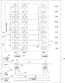
図1は本発明の第1の実施形態に係る固体撮像装置100の概略構成を示す図である。本実施形態に係る固体撮像装置100は例えばCMOSイメージセンサであり、被写体像を示す入射光を光電変換し、光電変換により得られた電気信号をデジタルデータとして外部に出力することで被写体の撮像を行う装置である。固体撮像装置100は、画素アレイ110、増幅回路120、A/D変換器130、垂直走査回路140、水平走査回路150、ランプ信号生成部170、カウンタ180、信号処理部190、及びタイミング制御部195を備える。
(First embodiment)
FIG. 1 is a diagram showing a schematic configuration of a solid-
画素アレイ110はマトリクス状に配置された複数の画素111、画素111の行ごとに共通化された行選択線112、画素111の列ごとに共通化された列信号線113、及び列方向加算平均スイッチ119を備える。各画素111はフォトダイオード等の光電変換素子を備え、固体撮像装置100への入射光の光電変換を行う。各画素の光電変換素子には所定の波長の入射光を選択的に透過する色フィルタが配置されている。図中の各画素111のR、Gr、Gb、Bの記号は、それぞれの画素111に赤、緑、緑、青の色フィルタが配置されていることを示している。本実施形態における色フィルタの色配列はベイヤ配列であり、2×2画素を1単位とする色フィルタの繰り返し配列となっている。
The
各画素111は行選択線112及び列信号線113と接続されており、各行選択線112は垂直走査回路140と接続され、各列信号線113は増幅回路120と接続されている。
Each
列方向加算平均スイッチ119は同色の色フィルタを備える画素111を接続する配線間に配置されている。列方向加算平均スイッチ119をオンにすると、列(垂直)方向に並ぶ同色の複数の画素111から出力される信号が加算平均される。したがって、列方向加算平均スイッチ119は画素111の信号を列(垂直)方向に加算平均する第1の加算回路として機能する。
The column direction
なお、本実施形態の説明では、画素アレイ110は図の左側から順に1列目、2列目、・・・n列目、図の下側から順に1行目、2行目、・・・9行目と呼称する。本願明細書の図面及びその説明における画素アレイ110は、その一部を抜き出した例示であり、全体を示すものではない。また、1行目、偶数行、奇数行といった記載により画素アレイ110の行及び列を特定することがあるが、これは説明のために図面中の位置を示すための便宜的な記載であり、実際の画素アレイ110の中の具体的な位置を特定することを意図するものではない。
In the description of the present embodiment, the
垂直走査回路140は画素行ごとに配置された行選択線112に駆動パルス信号を順番に供給する。行選択線112に駆動パルス信号が供給されると、対応する画素行に含まれる各画素111からは、光電変換された電荷がアナログの電圧信号として各列信号線113に読み出される。本実施形態の固体撮像装置100では、画素アレイ110から、画素111のリセットレベルの信号であるノイズ信号と、光電変換により発生した電荷の発生量に応じた信号にノイズ信号が重畳した画素信号とがアナログ信号として読み出される。画素信号の電圧からノイズ信号の電圧を減算することで、ノイズ信号が除去され、光電変換により発生した電荷に対応する電圧値を得ることができる。
The
各増幅回路120の入力端子は各列信号線113に接続され、出力端子は各A/D変換器130に接続される。増幅回路120は列信号線113を介して画素111から入力されたアナログ信号を増幅してA/D変換器130に対して出力する。
The input terminal of each
ランプ信号生成部170は、のこぎり波等の電圧が単調に変化する波形を有するランプ信号Vrampを生成し、ランプ信号線171を通じて各A/D変換器130に対して出力する。
The ramp
カウンタ180はカウントデータ線181を通じてカウント値Cntを各A/D変換器130に対して出力する。カウンタ180は時間とともに変化するカウント値を出力する回路であり、例えばグレイコードを出力するグレイカウンタや2進数を出力するバイナリカウンタを用いることができる。また、カウンタ180はアップダウン機能、すなわち、カウント値の上昇及び下降を切り替える機能を備えていてもよい。
The
A/D変換器130は増幅回路120から入力されたノイズ信号又は画素信号の電圧をランプ信号生成部170から入力されたランプ信号の電圧と比較する。電圧の大小関係が反転した時点における、カウンタ180から出力されたカウント値を出力値とすることにより、ノイズ信号又は画素信号はアナログデータからデジタルデータに変換される。
The A /
なお、本実施形態では複数のA/D変換器130が、ランプ信号生成部170及びカウンタ180を共有しているが、A/D変換器130ごとに個別にこれらの構成要素を有してもよい。
In the present embodiment, the plurality of A /
水平走査回路150はA/D変換器130から出力されるデジタルデータを列ごとにデジタル信号線191、192に転送する。デジタル信号線191にはノイズ信号を表すデジタルデータが、デジタル信号線192には画素信号を表すデジタルデータがそれぞれ伝送され、それぞれ信号処理部190に入力される。信号処理部190は画素信号を表すデジタルデータからノイズ信号を表すデジタルデータを減算して、光電変換により発生した電荷に対応する値を外部に出力する。
The
タイミング制御部195は、上述の各構成要素にパルス信号を供給して固体撮像装置100の動作を制御する。タイミング制御部195から各構成要素へのパルス信号の送信は信号線(不図示)を介して行われる。
The
本実施形態では固体撮像装置100が増幅回路120を含んでいるため、画素信号等は増幅されてからA/D変換器130に入力される。したがって、A/D変換器130で発生するノイズの影響は軽減される。しかしながら、固体撮像装置100の増幅回路120を省略することにより、画素111からのアナログ信号が列信号線113を介して直接にA/D変換器130へ供給されてもよい。この場合、上述の増幅回路120を備えた構成よりも素子数を削減することができる。
In the present embodiment, since the solid-
また、図1に示した例では画素アレイ110の一方の側に増幅回路120、A/D変換器130及び水平走査回路150が配置さるように図示されている。しかしながら、これらの構成要素が画素アレイ110の両側に配置され、画素列ごとにいずれか一方の側の構成要素に振り分けられるよう構成してもよい。当該構成では、上述の実施形態よりも走査速度を向上することができる。
In the example illustrated in FIG. 1, the
図2は画素111の等価回路を示す図である。図2は図1に示す画素アレイ110の1行目と3行目と5行目の画素111の1列分を抜き出し、その等価回路を図示している。画素111は光電変換を行うフォトダイオード114及び複数のトランジスタを含む。複数のトランジスタは転送スイッチ115、リセットスイッチ116、増幅トランジスタ117及び行選択スイッチ118を含み、フォトダイオードで発生した電荷量をアナログ信号として列信号線113に出力するためのスイッチング機能及び増幅機能を有する。転送スイッチ115、リセットスイッチ116、増幅トランジスタ117及び行選択スイッチ118は、例えばNチャネル型の電界効果トランジスタ等のトランジスタにより構成される。また、転送スイッチ115、リセットスイッチ116、増幅トランジスタ117の間には、保持した電荷を検出するためのフローティングディフュージョンFDが構成されている。
FIG. 2 is a diagram showing an equivalent circuit of the
なお、「スイッチ」及び「トランジスタ」の用語の使い分けは、各トランジスタがスイッチング機能及び増幅機能のいずれを主に利用しているかを示すことで回路動作の理解を助けるためのものであり、素子の構造を限定することを意図するものではない。 The terminology of “switch” and “transistor” is used to help understand the circuit operation by indicating which of the switching function and amplification function each transistor mainly uses. It is not intended to limit the structure.
フォトダイオード114は転送スイッチ115を介してフローティングディフュージョンFDに接続される。フローティングディフュージョンFDはまた、リセットスイッチ116を介して電圧源SVDDに接続されるとともに、増幅トランジスタ117のゲート電極に接続される。増幅トランジスタ117の第1主電極は電圧源SVDDに接続され、増幅トランジスタ117の第2主電極は行選択スイッチ118を介して列信号線113に接続される。
The
行選択スイッチ118のゲート電極は行制御線112の1つであり、信号を読み出す行を選択するための信号を伝送する行選択線PSEL(不図示)に接続される。リセットスイッチ116のゲート電極は、行制御線112の1つであり、リセット信号を伝送するリセット線PRES(不図示)に接続される。また、転送スイッチ115のゲート電極は、行制御線112の1つであり、フォトダイオード114で発生した電荷を転送するための信号を伝送する転送線PTX(不図示)に接続される。
The gate electrode of the
本実施形態においては、1つの画素111につき、2つのフォトダイオード114が含まれており、またそれぞれに対し転送スイッチ115が接続されている。そのため、各フォトダイオード114で発生した光電荷は選択的にフローティングディフュージョンFDに転送される。
In the present embodiment, each
各フォトダイオードは、独立に光電荷を蓄積し、各転送スイッチ115は独立に光電荷を転送することができる。本実施形態の画素111は、フォトダイオード114及び転送スイッチ115を2組備える。すなわち、画素111は、フォトダイオード114と転送スイッチ115をそれぞれ有する分割画素201A及び201Bを小単位として備える。
Each photodiode accumulates photocharges independently, and each
縦方向に隣りあう同色の画素111の間には、複数の画素111の複数のフローティングディフュージョンFDを接続して、電荷を加算平均するための列方向加算平均スイッチ119が設けられている。
Between the
転送スイッチ115を開閉することにより、列方向加算平均スイッチ119を介して接続された複数のフローティングディフュージョンFDに光電荷が転送される。各フローティングディフュージョンFDは接続されているため、転送された電荷は各フローティングディフュージョンFDに分配され、同一の電圧となる。すなわち、各フローティングディフュージョンFDに転送された電荷が加算平均される。このようにして、列方向加算平均スイッチ119は画素111の信号を列(垂直)方向に加算平均する第1の加算回路として機能する。この加算平均により画素信号のノイズ信号を低減することができる。
By opening and closing the
さらに、加算平均により1フレームに読み出す出力数を圧縮することが可能となるため、高フレームレートが達成できる。例えば、垂直及び水平方向の2x2画素を加算平均した場合、4k2kフォーマットをHDフォーマットに変換することができ、フレームレートを向上することができる。 Furthermore, since the number of outputs to be read in one frame can be compressed by addition averaging, a high frame rate can be achieved. For example, when 2x2 pixels in the vertical and horizontal directions are added and averaged, the 4k2k format can be converted to the HD format, and the frame rate can be improved.
例えば、図1において、4行目と6行目に配置された列(垂直)方向のGb画素及びB画素の2つをそれぞれ1:1の重みで加算平均する。そして、列方向に隣接する1行目、3行目及び5行目に配置されたR画素及びGr画素の3つをそれぞれ1:2:1の重みで加算平均する。すなわち、各分割画素から出力され、加算される信号の個数が、加算対象となる画素ごとに異なっている。そうすると、加算平均後の出力信号に含まれる画素の重心位置が等ピッチ(2画素ピッチ)に並ぶため、撮影した画像の被写体のエッジ部に不自然な色がつく偽色などの不具合を避けることができ、良好な画像が得られる。ただし、加算平均に用いる画素数や重みはこれに限定されるものではない。なお、本願明細書で用いる重み付け平均化した信号の「重心位置」とは、重み付け平均化に用いた信号のアドレスを同じ比率で重み付け平均して得たアドレスを意味する。例えば、信号Xのアドレスを(X1、X2)で信号Yのアドレスを(Y1、Y2)とすると、信号Xと信号Yの1:2平均化信号の重心位置は((X1+2Y1)/3、(X2+2Y2)/3)である。 For example, in FIG. 1, two Gb pixels and B pixels in the column (vertical) direction arranged in the fourth and sixth rows are added and averaged with a weight of 1: 1, respectively. Then, the three R pixels and Gr pixels arranged in the first row, the third row, and the fifth row adjacent in the column direction are added and averaged with a weight of 1: 2: 1, respectively. That is, the number of signals output from each divided pixel and added is different for each pixel to be added. Then, the center of gravity of the pixels included in the output signal after the averaging is aligned at an equal pitch (2 pixel pitch), so that it is possible to avoid problems such as a false color in which an unnatural color is formed on the edge of the subject of the photographed image. And a good image can be obtained. However, the number of pixels and the weight used for the averaging are not limited to this. Note that the “center of gravity position” of the weighted average signal used in the specification of the present application means an address obtained by weighted average of the address of the signal used for weighted average at the same ratio. For example, if the address of the signal X is (X 1 , X 2 ) and the address of the signal Y is (Y 1 , Y 2 ), the centroid position of the 1: 2 average signal of the signal X and the signal Y is ((X 1 + 2Y 1 ) / 3, (X 2 + 2Y 2 ) / 3).
図3は画素111の素子構造を示す平面図である。2つのフォトダイオード114は、同一色の色フィルタ200で覆われている。さらに画素上には、集光機能を有する光学系としてマイクロレンズ202が配置されている。2つの分割画素201A及び201Bは、同一のマイクロレンズ202を共有している。マイクロレンズの中心は2つの分割画素の中間又は略中間に位置しており、図3で示すような2つの分割画素の光検出感度の入射角依存性は異なったものとなる。この入射角依存性の違いを利用して被写体の距離情報を得ることができ、例えばオートフォーカスなどの機能に利用することができる。
FIG. 3 is a plan view showing the element structure of the
図4は画素111の画素信号の読み出し動作を示す駆動タイミング図である。
FIG. 4 is a drive timing chart showing a pixel signal readout operation of the
図4の読出し動作では、列方向の同色画素111が1:2:1に重みづけ加算平均される。すなわち、図1に示した画素アレイ110の1行目、3行目及び5行目のR画素同士とGr画素同士をそれぞれ重みづけ加算平均し、次に5行目、7行目及び9行目の画素を同様に重みづけ加算平均する。このようにして、垂直方向の画素出力数を1/2に圧縮して読み出すことができる。図4では1行目と3行目と5行目の画素を重みづけ加算平均する駆動タイミング図である。
In the read operation of FIG. 4, the
図4に示した駆動タイミングを時間順に説明する。なお、本明細書の説明においては、各トランジスタ(スイッチ)はゲート電極に入力される信号電圧がハイレベルのときにソース電極とドレイン電極が導通状態(オン)になるとする。 The drive timing shown in FIG. 4 will be described in order of time. Note that in the description of this specification, it is assumed that the source electrode and the drain electrode of each transistor (switch) are in a conductive state (ON) when the signal voltage input to the gate electrode is at a high level.
まず時刻t0において、1行目、3行目及び5行目の行選択信号SEL1、SEL2及びSEL3がハイレベルとなり、各増幅トランジスタ117がオンになる。このとき、対応する3行の増幅トランジスタ117が列信号線113に接続され、それぞれソースフォロワ回路として動作する。すなわち、フローティングディフュージョンFDの電位に相当する電圧が列信号線113に出力される。同時刻t0にリセット信号RES1、RES2及びRES3がハイレベルとなり、各リセットスイッチがオンになる。3行のフローティングディフュージョンFDの電位は、リセットトランジスタ116を介して、電圧源SVDDの電位にリセットされる。さらに、同時刻t0に各列方向加算平均スイッチ119の制御信号SUM1、SUM2がハイレベルとなり、各列方向加算平均スイッチ119はオンとなる。この状態は時刻t6まで継続する。すなわち、一連の読み出し動作が終わる時刻t6まで、1行目、3行目及び5行目の各フローティングディフュージョンFDは電気的に接続され、同電位となる。
First, at time t0, the row selection signals SEL1, SEL2, and SEL3 of the first row, the third row, and the fifth row are at a high level, and each
時刻t1において、リセット信号RES1、RES2及びRES3がローレベルとなり、各リセットトランジスタ116がオフになる。このとき、3つの行のフローティングディフュージョンFDの電圧はリセット電圧、すなわち電圧源SVDDの電位である。したがって、増幅用トランジスタ117から列信号線113に出力される信号は、フォトダイオード114から電荷が転送されていないときの電圧信号、すなわちノイズ信号となる。これをN信号とする。N信号は増幅回路120で増幅されたのち、AD変換器130でデジタル信号に変換される。
At time t1, the reset signals RES1, RES2, and RES3 become low level, and each
次に、時刻t2〜t3において転送信号TXA1、TXA2がハイレベルとなり、1行目及び3行目の分割画素201Aの信号が転送トランジスタ115を介して読み出され、フローティングディフュージョンFD上で加算平均される。この信号は増幅用トランジスタ117を介して列信号線113に出力される。時刻t2〜t3における列信号線113からの出力信号は上述のN信号に分割画素Aの光電荷が重畳されたものに相当する電圧である。これをN+A信号とする。N+A信号も、N信号と同様に、増幅回路120で増幅されたのち、A/D変換器130でデジタル信号に変換される。すなわち、N+A信号の電圧は、1行目の分割画素201A及び3行目の分割画素201Aから出力された電荷をフローティングディフュージョンFD上で加算平均して得られた電圧に相当する。
Next, at time t2 to t3, the transfer signals TXA1 and TXA2 become high level, the signals of the divided
次に、時刻t4からt5において、転送信号TXB2及びTXB3がハイレベルとなり、3行目及び5行目の分割画素201Bの信号が、転送トランジスタ115を介して読み出され、フローティングディフュージョンFD上で同様に加算平均される。このとき、上述のA+N信号に分割画素201Bから出力された光電荷による信号が重畳されたものに相当する電圧が出力される。これをN+A+B信号とする。N+A+B信号も、N信号及びN+A信号と同様に、増幅回路120で増幅されたのち、A/D変換器130でデジタル信号に変換される。
Next, from time t4 to t5, the transfer signals TXB2 and TXB3 become high level, the signals of the divided
次に、時刻t6において、SEL1、SEL2、SEL3、SUM1及びSUM2がローレベルとなり、行選択スイッチ118及び列方向加算平均スイッチ119がすべてオフとなり、一連の読み出し動作が終了する。
Next, at time t6, SEL1, SEL2, SEL3, SUM1, and SUM2 are at a low level, the
引き続き、時刻t7〜t13において、同様な動作が5行目、7行目、9行目において、繰り返し行われる。 Subsequently, at times t7 to t13, the same operation is repeatedly performed on the fifth, seventh, and ninth lines.
N+A+B信号に寄与する電荷は、1行目の分割画素201Aからの電荷、3行目の分割画素201A及び201Bからの電荷、並びに5行目の分割画素201Bからの電荷を加算したものである。すなわち、それぞれの行での加算平均に寄与する分割画素数は、1:2:1になっている。
The charge contributing to the N + A + B signal is the sum of the charge from the divided
上述のとおり、3行目では分割画素201A及び201Bからの電荷が2回に分けて読み出される。1回目(時刻t2〜t3)は分割画素201A、2回目(時刻t4〜t5)は分割画素201Bの信号がそれぞれ読み出されるため、1回目と2回目の読み出しでは異なるフォトダイオード114から生成された電荷が信号として読み出される。つまり、分割画素の画素内における相対位置が、加算対象となる複数の画素によって異なっている。このようにして、同じフォトダイオードから電荷を読み出さなくても同じ画素から2回信号を読み出すことが可能となり、1:2:1重みづけ加算平均が実現される。
As described above, in the third row, the charges from the divided
重みづけ加算を伴わない平均化のみを行った場合、平均化を行う画素の重心位置(加算平均化信号に含まれる画素のアドレスの重心位置)は等ピッチとはならない。これに対し、上述の1:2:1重みづけ平均と4行目及び6行目の画素の1:1加算平均との組み合わせにより、加算平均される画素の重心位置が等ピッチとなる。これにより、本実施形態の固体撮像装置100を用いることで、被写体のエッジ部において顕著となる不自然な色づき(偽色)が従来に比べ低減された、スキャナ、デジタルビデオカメラ、デジタルスチルカメラ等の撮像システムが実現できる。
When only averaging without weighted addition is performed, the barycentric position of the pixel to be averaged (the barycentric position of the address of the pixel included in the addition averaged signal) is not equal pitch. On the other hand, the center-of-gravity positions of the pixels to be averaged are equal pitches by the combination of the above-described 1: 2: 1 weighted average and the 1: 1 addition average of the pixels in the fourth and sixth rows. Thereby, by using the solid-
1行目と5行目の信号を読み出す分割画素はそれぞれ分割画素201Aと分割画素201Bである。すなわち、1行目と5行目では、列方向に半ピッチ分だけ位置が異なるフォトダイオード114から電荷を取得することになる。分割画素の位置の差が撮影した画像の画質に影響を与える可能性について検討する。
The divided pixels from which signals in the first row and the fifth row are read are divided
被写体にコントラストパタン(縞模様のパタン)がない場合は、分割画素201A及び201Bから出力される2つの信号は同等と考えられる。被写体に行方向のコントラストパタン(横縞模様のパタン)がある場合においても2つの信号は同等と考えられる。
When the subject has no contrast pattern (striped pattern), the two signals output from the divided
被写体に列方向のコントラストパタン(縦縞模様のパタン)がある場合にも、画素ピッチに近いコントラストをもつ非常に細かい被写体でない限り、1行目、3行目及び5行目の分割画素201Aと分割画素201Bの出力電荷量の比は同等と考えられる。結果として、コントラストパタンを撮影した場合でも不自然な色づきが発生する可能性は低く、分割画素201Aと分割画素201Bの位置の差は問題にならないと考えられる。したがって、コントラストパタンの撮影において、本実施形態は従来技術と比較して有利であると考えられる。
Even if the subject has a contrast pattern in the column direction (vertical striped pattern), it is divided into the divided
一方、撮影条件の最適化のために必要な距離情報を得るため、分割画素201A及び分割画素201Bの信号を個別に取得することもできる。N信号とN+A信号の差分を信号処理部190において計算することで、2行分の分割画素201Aの出力信号を加算平均した信号(A信号)を得ることができる。さらに、N信号とN+A+B信号の差分を信号処理部190において計算してA+B信号を得たのち、前述の方法で取得したA信号の加算平均信号をさらに減算することで、2行分の分割画素201Bの出力信号を加算平均した信号(B信号)を得ることができる。このようにして計算されたA信号及びB信号は加算平均によりS/N比(Signal/Noise比)が改善しているため、高精度な距離情報が得られ、より安定したオートフォーカスが実行できる。
On the other hand, in order to obtain distance information necessary for optimizing the shooting conditions, the signals of the divided
この方法は位相差検出法によるオートフォーカスに用いることが好適である。本実施形態では、複数画素にまたがる分割画素201Aの信号群で取得される緩やかなシェーディングと分割画素201Bの信号群で取得される緩やかなシェーディングとの僅かなずれを位置方向の位相差として検知することで、距離情報を取得することができる。A信号及びB信号は、上述の理由によりS/N比が改善しているので、この方法によりオートフォーカスの安定化が実現される。
This method is preferably used for autofocus by the phase difference detection method. In the present embodiment, a slight shift between the gentle shading acquired by the signal group of the divided
本実施形態においては、フォトダイオードを行(水平)方向に分割しているため、行方向に輝度差が生じる撮影シーンにおいては位相差検出をさらに有効に行うことができる。これに対し、信号の重みづけ加算平均は、列方向に行われる。そのため、加算平均による空間分解能の損失なくS/N比を向上することができる。 In the present embodiment, since the photodiode is divided in the row (horizontal) direction, phase difference detection can be performed more effectively in a shooting scene in which a luminance difference occurs in the row direction. On the other hand, weighted averaging of signals is performed in the column direction. Therefore, the S / N ratio can be improved without loss of spatial resolution due to the averaging.
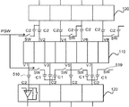
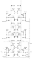
次に、行(水平)方向の重み付け加算平均について説明する。図5は各列からの色信号を行(水平)方向に重みづけ加算平均化する回路を示す図である。加算平均は画素アレイ110と増幅回路120の間に配置された、複数の行方向加算平均スイッチ519及び複数の入力容量510によって行われる。複数の行方向加算平均スイッチ519はタイミング制御部195からの駆動信号PSWによって、それぞれ個別にオン又はオフに制御される。画素アレイ110の各列の画素111から列信号線113に読み出された画素信号は複数の入力容量510を介して増幅回路120に入力される。図5に部分的に図示している8個の画素アレイ110のそれぞれの出力電圧をV1・・・V8とする。
Next, the weighted average in the row (horizontal) direction will be described. FIG. 5 is a diagram showing a circuit for weighting and averaging the color signals from each column in the row (horizontal) direction. The addition averaging is performed by a plurality of row direction addition average switches 519 and a plurality of
図5において、奇数列の画素(R又はGb)から出力された信号は画素アレイ110の下方向に、偶数列からの画素(Gr又はB)から出力された信号は画素アレイ110の上方向に設けた増幅回路120に入力されるように記載されている。ただし、このように奇数列と偶数列を分けて図面を記載した目的は加算回路における加算平均の動作の理解を容易にするためであり、実際の回路上での配置は図5と異なっても良い。例えば、奇数列と偶数列を上下に分けず、1方向に引き出しても良い。
In FIG. 5, signals output from the pixels (R or Gb) in the odd columns are downward in the
複数の入力容量510は容量値C1の容量(以下、容量C1と呼ぶ)と容量値C2の容量(以下、容量C2と呼ぶ)とを含む。画素アレイ110のn列目の画素列は、容量C2を介してn列目の増幅回路120と接続される。
The plurality of
例えば、1列目の画素111は、行方向加算平均スイッチ519及び容量C1を介して3列目の増幅回路120と接続される。3列目の増幅回路120は行方向加算平均スイッチ519及び容量C1を介して5列目の画素111と接続される。以降の画素についても同様である。すなわち、奇数列においては4n−1列目の増幅回路に対し、容量C2を介して4n−1列目の画素が接続されていることに加えて、4n−3列目と4n+1列目の画素も行方向加算平均スイッチ519及び容量C1を介して接続されている。
For example, the
一方、偶数列の画素は異なる接続方法となっている。例えば、6列目の増幅回路は、行方向加算平均スイッチ519及び容量C2を介して4列目の画素と接続される。すなわち、偶数列においては4n+2列目の増幅回路に対し、容量C2を介して4n+2列目の画素が接続されていることに加えて、4n列目の画素が行方向加算平均スイッチ519及び容量C2を介して接続されている。
On the other hand, even-numbered pixels have different connection methods. For example, the amplifier circuit in the sixth column is connected to the pixels in the fourth column via the row direction addition
このような回路構成とすることで、画素信号の加算平均化が実現される。本実施形態においては、一例として容量C1を容量C2の1/2の容量値とする。駆動信号PSWによって、行方向加算平均スイッチ519がONになると、容量値の比率にしたがって電圧が平均化される。よって、3列目の増幅回路120に印加される電圧は(V1+2×V3+V5)/4となり、6列目の増幅回路120に印加される電圧は(V4+V6)/2となる。すなわち、奇数列からの1列目と3列目と5列目の画素信号は1:2:1の加算平均化が行われ、偶数列からの4列目と6列目の画素信号は1:1の加算平均化が行われる。このようにして、行方向加算平均スイッチ519及び入力容量510は、画素111の信号を行(水平)方向に加算平均する第2の加算回路として機能する。
With such a circuit configuration, the pixel signals are averaged. In the present embodiment, as an example, the capacitance C1 is set to a capacitance value that is ½ of the capacitance C2. When the row direction addition
なお、行方向加算平均スイッチ519がOFFの場合は、加算平均を行わずすべての画素からそのまま色信号を読み出す回路として機能する。このようにして、各画素の出力信号を重み付け加算平均をせずに出力することも可能である。
When the row direction addition
増幅回路の入力容量によって信号の加算平均を行う方法を説明したが、A/D変換回路の後段に加算平均を行う回路を設けることにより、A/D変換後のデータを加算平均化しても良い。 Although the method of performing the averaging of the signals according to the input capacitance of the amplifier circuit has been described, the data after the A / D conversion may be averaged by providing a circuit for performing the averaging in the subsequent stage of the A / D conversion circuit. .
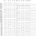
これまで説明した、列(垂直)方向及び行(水平)方向の重み付け加算平均について画素のアドレスの観点で整理して説明する。図6(A)〜(D)は、列方向と行方向の色信号の重みづけ加算平均化を示す図である。 The above-described weighted average in the column (vertical) direction and the row (horizontal) direction will be described in terms of pixel addresses. 6A to 6D are diagrams illustrating weighted addition averaging of color signals in the column direction and the row direction.
図6(A)は各画素の色フィルタの配置、すなわち各画素から得られる色信号の配列を示す図である。表中の(R、Gb、Gr、B)がそれぞれ(赤、緑、緑、青)の色信号に対応する。また、垂直方向に並ぶ数値が各行のアドレス番号、水平方向に並ぶ数値が各列のアドレス番号を表しており、行と列のアドレス番号を指定することで、各画素の位置とその画素から得られる色信号を特定できる。以下、例えば、第3行の第1列に配置されたRの色信号をR(31)のように表記することもある。 FIG. 6A is a diagram showing the arrangement of color filters for each pixel, that is, the arrangement of color signals obtained from each pixel. (R, Gb, Gr, B) in the table respectively correspond to (red, green, green, blue) color signals. The numerical values arranged in the vertical direction represent the address numbers of the respective rows, and the numerical values arranged in the horizontal direction represent the address numbers of the respective columns. By specifying the address numbers of the row and the column, the position of each pixel and the pixel obtained from that pixel are obtained. Color signal to be specified Hereinafter, for example, the R color signal arranged in the first column of the third row may be expressed as R (31).
図6(A)の欄外に付記した符号は、上述した垂直方向の画素信号の加算平均化の比率である。すなわち、各列内で、奇数行の1行目、3行目及び5行目の色信号には1:2:1加算平均が行われる。そして次に5行目、7行目及び9行目の色信号にも1:2:1加算平均が行われることを示している。ここで1:2:1の「1」に対応する信号はA信号又はB信号のいずれかであり、「2」に対応する信号はA信号及びB信号を加算したものである。また、偶数行においては4行目と6行目の色信号の1:1加算平均化が行われるが、ここでの1:1の「1」に対応する信号はA信号及びB信号を加算したものである。 The reference numerals appended to the outside of FIG. 6A are the above-described ratios of averaging of pixel signals in the vertical direction. That is, 1: 2: 1 addition averaging is performed on the color signals of the first, third, and fifth rows of the odd rows within each column. Then, it is shown that the 1: 2: 1 addition averaging is also performed on the color signals of the 5th, 7th, and 9th rows. Here, the signal corresponding to “1” of 1: 2: 1 is either the A signal or the B signal, and the signal corresponding to “2” is the sum of the A signal and the B signal. In addition, in the even-numbered row, the 1: 1 addition and averaging of the color signals in the fourth and sixth rows is performed, but the signal corresponding to “1” of 1: 1 here adds the A signal and the B signal. It is a thing.
引き続いて8行目と10行目の色信号の1:1加算平均化が行われる。 Subsequently, 1: 1 addition averaging of the color signals in the 8th and 10th rows is performed.
次に、水平方向において行われる加算平均化を図6(B)に示す。図6(B)の表は上述の垂直方向の加算平均化後の新たな色信号の配列を示す。水平方向の色信号についても、垂直方向と同様に奇数列のR信号とGb信号は1:2:1の、偶数列のGrとB信号は1:1の加算平均化が行われる。 Next, addition averaging performed in the horizontal direction is shown in FIG. The table in FIG. 6B shows a new color signal arrangement after the above-mentioned vertical averaging. As for the color signals in the horizontal direction, the R and Gb signals in the odd number columns are 1: 2: 1 and the Gr and B signals in the even number columns are added and averaged in the same manner as in the vertical direction.
図6(C)は垂直と水平方向に加算平均した後の色信号R(33)、Gr(35)、Gb(35)、B(55)の空間的配置を図6(A)の行と列アドレス番号に対応して示した図である。加算平均後の各アドレス番号は、加算平均に用いられた元の色信号のアドレスの重心位置に対応する。例えば、1行目、3行目及び5行目の色信号を1:2:1加算平均し、次に1列目、3列目及び5列目の色信号を1:2:1加算平均した場合、その重心位置は(33)なので、加算平均した後の色信号はR(33)と表記されている。このように、図6(A)の各画素の垂直方向と水平方向の色信号がそれぞれ1/2に圧縮された色信号を得る。R(33)、Gr(35)、Gb(35)、B(55)の加算平均化に寄与する色信号の配置を図6(D)に示す。 FIG. 6C shows the spatial arrangement of the color signals R (33), Gr (35), Gb (35), and B (55) after averaging in the vertical and horizontal directions as the row in FIG. It is the figure shown corresponding to the column address number. Each address number after the averaging process corresponds to the barycentric position of the address of the original color signal used for the averaging process. For example, the color signals of the first row, the third row, and the fifth row are averaged 1: 2: 1, and then the color signals of the first column, the third column, and the fifth column are averaged 1: 2: 1. In this case, since the center of gravity position is (33), the color signal after the averaging is expressed as R (33). In this way, a color signal is obtained in which the vertical and horizontal color signals of each pixel in FIG. FIG. 6D shows the arrangement of color signals that contribute to the averaging of R (33), Gr (35), Gb (35), and B (55).
上述の各色信号の加算平均化について、数式により整理して表現すると次式のようになる。ただし、この式でAmnはアドレス(m、n)の画素111から出力されるA信号、Bmnはアドレス(m、n)の画素111から出力されるB信号を意味する。
R(33)=(1列目の1、3、5行の加算)+2×(3列目の1、3、5行の加算)+
(5列目の1、3、5行の加算)
={B11+(A31+B31)+A51}+2×{B13+(A33+B33)+A53}+
{B15+(A35+B35)+A55}
Gr(35)=(4列目の1、3、5行の加算)+(6列目の1、3、5行の加算)
={B14+(A34+B34)+A54}+{B16+(A36+B36)+A56}
Gb(53)=(1列目の4、6行の加算)+2×(3列目の4、6行の加算)+(5列
目の4、6行の加算)
={(A41+B41)+(A61+B61)}+2×{(A43+B43)+(A63+
B63)}+{(A45+B45)+(A65+B65)}
B(55)=(4列目の4、6行の加算)+(6列目の4、6行の加算)
={(A44+B44)+(A64+B64)}+{(A46+B46)+(A66+B66)
}
The addition averaging of the above-described color signals can be expressed by the following equation when organized and expressed by equations. In this equation, A mn means the A signal output from the
R (33) = (addition of 1, 3, 5 rows in the first column) + 2 × (addition of 1, 3, 5 rows in the third column) +
(Addition of 1, 3, 5 rows in the fifth column)
= {B 11 + (A 31 + B 31 ) + A 51 } + 2 × {B 13 + (A 33 + B 33 ) + A 53 } +
{B 15 + (A 35 + B 35) + A 55}
Gr (35) = (addition of 1, 3, 5 rows in the fourth column) + (addition of 1, 3, 5 rows in the sixth column)
= {B 14 + (A 34 + B 34) + A 54} + {
Gb (53) = (addition of 4th and 6th rows in the first column) + 2 × (addition of 4th and 6th rows in the third column) + (5th column)
4th and 6th line addition)
= {(A 41 + B 41 ) + (A 61 + B 61 )} + 2 × {(A 43 + B 43 ) + (A 63 +
B63 )} + {( A45 + B45 ) + ( A65 + B65 )}
B (55) = (addition of 4th and 6th rows in the fourth column) + (addition of 4th and 6th rows in the sixth column)
= {( A44 + B44 ) + ( A64 + B64 )} + {( A46 + B46 ) + ( A66 + B66 )
}
以上説明したように、本実施形態の固体撮像装置によれば、画素信号の重みづけ加算平均化をすることで、加算平均を行う画素の重心位置が制御でき、エッジ部の偽色の発生が少なく、高フレームレートの画像出力が得られる。さらに、加算前の分割画素単体の信号を読み出しの過程で得ることが可能である。加算前の分割画素単体の信号を用いることにより、S/N比の高い位相差情報が得られ、この位相差情報を用いることで安定したオートフォーカスが可能となる。また、分割画素の信号を加算平均しているため、加算後のN+A+B信号には分割画素A、B間の位相差情報が残らない。これにより、不自然な画像となることが避けられる。 As described above, according to the solid-state imaging device of the present embodiment, by performing weighted addition averaging of pixel signals, it is possible to control the barycentric position of the pixels for which addition averaging is performed, and generation of false colors at the edge portion. Less image output with a high frame rate can be obtained. Furthermore, it is possible to obtain a signal of a single divided pixel before addition in the process of reading. By using a signal of a single divided pixel before addition, phase difference information with a high S / N ratio is obtained, and stable autofocus is possible by using this phase difference information. Further, since the signals of the divided pixels are added and averaged, the phase difference information between the divided pixels A and B does not remain in the N + A + B signal after the addition. This avoids an unnatural image.
(第2の実施形態)
本発明の第2の実施形態に係る固体撮像装置を以下に詳細に述べる。本実施形態は、第1の実施形態に対して画素の構成と列ごとに配置されている増幅回路の構成が異なるため、これらについてのみ詳細に説明する。
(Second Embodiment)
The solid-state imaging device according to the second embodiment of the present invention will be described in detail below. This embodiment is different from the first embodiment in the configuration of the pixels and the configuration of the amplifier circuit arranged for each column, and only these will be described in detail.
図7は、本発明の第2の実施形態に係る画素711の等価回路を示す図である。画素711は2分割ではなく、4分割の分割画素701A、701B、701C及び701Dを備える。さらにこれらの分割画素701A〜Dから信号を読み出すための、リセットスイッチ116、増幅トランジスタ117及び行選択スイッチ118はそれぞれ2系統配置されている。これらの点が第1の実施形態に対する構造上の差異点である。画素711は4つのフォトダイオード114を有する。分割画素701A及び701Cに含まれる2つのフォトダイオードは転送スイッチ115を介して増幅トランジスタ117と接続される。分割画素701B及び701Dに含まれる2つのフォトダイオードは、別系統の転送スイッチ115を介して増幅トランジスタ117と接続される。
FIG. 7 is a diagram showing an equivalent circuit of the
このように画素711は2系統の読み出し回路を有するので、1つの画素711には2つの列信号線113が設けられている。
In this manner, the
同系統内に配置されたフォトダイオードで発生した電荷は、第1の実施形態と同様にして画素711内での加算及び加算平均スイッチ119を介して接続された画素間での加算が可能である。
Charges generated by the photodiodes arranged in the same system can be added in the
図8は本発明の第2の実施形態に係る画素711の素子構造を示す平面図である。4分割された分割画素に含まれる4つのフォトダイオード114は同一色の色フィルタ200及び同一のマイクロレンズ202を共有している。
FIG. 8 is a plan view showing an element structure of a
図9は、4分割画素から垂直方向に並ぶ分割画素間の位相差信号を取得しながら、各画素の加算信号を得る、第1の駆動タイミング図である。図4に示した第1の実施形態に係る駆動タイミング図との差異点は、転送スイッチを制御する転送信号TXA1〜5及びTXB1〜5が、TXA1/B1〜A5/B5及びTXC1/D1〜C5/D5に置き換えられている点である。ここで、TXA1/B1等の表記は両方の転送スイッチをオン又はオフする信号を送信することを意味する。すなわち、分割画素701Aと分割画素701Bの信号は同時に転送され、分割画素701Cと分割画素701Dの信号も同時に転送される。したがって、同時に転送される信号によって動作する2つの画素を同一視すれば、垂直に2分割された画素として考えることができる。そうすると、大部分の動作は第1の実施形態と同様であるため、本実施形態のポイントとなる動作のみを説明する。なお、以下の説明において、分割画素701A〜Dより出力される信号をそれぞれA〜D信号と呼ぶ。
FIG. 9 is a first drive timing chart in which an addition signal of each pixel is obtained while obtaining a phase difference signal between divided pixels arranged in the vertical direction from the four divided pixels. The difference from the drive timing chart according to the first embodiment shown in FIG. 4 is that the transfer signals TXA1 to TXB1 and TXB1 to 5 that control the transfer switches are TXA1 / B1 to A5 / B5 and TXC1 / D1 to C5. / D5. Here, a notation such as TXA1 / B1 means that a signal for turning on or off both transfer switches is transmitted. That is, the signals of the divided
まず、時刻t2〜t3において、分割画素701A及び701Bの信号が読み出され、N+A+B信号が取得される。時刻t4〜t5において、分割画素701C及び701Dの信号が出力され、N+A+B信号に重畳されることで、N+A+B+C+D信号が取得される。第1の実施形態と同様に垂直方向の分割画素間の位相差信号が取得される。同時に、第1の実施形態と同様に垂直方向に並ぶ画素間の信号はフローティングディフュージョンで加算平均され、水平方向に並ぶ画素間の信号は増幅回路120において、1:2:1加算平均される。
First, at times t2 to t3, signals of the divided
図10は、4分割画素から水平方向に並ぶ分割画素間の位相差信号を取得しながら、各画素の加算信号を得る、第2の駆動タイミング図である。図9に示した駆動タイミング図との差異点は、転送スイッチを制御する転送信号TXA1/B1〜A5/B5及びTXC1/D1〜C5/D5が、TXA1/C1〜A5/C5及びTXB1/D1〜B5/D5に置き換えられている点である。すなわち、分割画素701Aと分割画素701Cの信号は同時に転送され、分割画素701Bと分割画素701Dの信号も同時に転送される。よって、水平に2分割された画素と考えることができる。つまり、図9に対して水平方向と垂直方向の分割の仕方を入れ替えたものと考えることもできる。したがって同様に、水平方向の位相差信号と同時に、重みづけ加算平均出力を得ることができる。
FIG. 10 is a second drive timing chart in which an addition signal of each pixel is obtained while obtaining a phase difference signal between divided pixels arranged in the horizontal direction from the four divided pixels. The difference from the drive timing chart shown in FIG. 9 is that the transfer signals TXA1 / B1 to A5 / B5 and TXC1 / D1 to C5 / D5 for controlling the transfer switches are changed to TXA1 / C1 to A5 / C5 and TXB1 / D1. It is a point replaced with B5 / D5. That is, the signal of the divided
本実施形態の固体撮像装置によれば、図9又は図10に示した2種類の駆動タイミングのいずれかを選択的に設定することで、4分割画素からなる画素111より水平又は垂直方向の任意の位相差信号を取得しつつ、2x2加算信号を取得することができる。 According to the solid-state imaging device of the present embodiment, any one of the two types of drive timings shown in FIG. 9 or FIG. The 2 × 2 addition signal can be acquired while acquiring the phase difference signal.
なお、本実施形態では位相差信号の取得と加算平均出力の取得を同時に行ったが、分割画素の一部を読み出す低感度出力と全部の分割画素を読み出す高感度の加算平均出力の2種を出力するように構成することもできる。これらを併用することで、光検出のダイナミックレンジを拡張することができる。 In the present embodiment, the acquisition of the phase difference signal and the acquisition of the average output are performed simultaneously. However, there are two types of low-sensitivity output that reads out a part of the divided pixels and high-sensitivity addition average output that reads out all the divided pixels. It can also be configured to output. By using these together, the dynamic range of light detection can be expanded.
(第3の実施形態)
図11は、本発明の第1又は第2の実施形態に係る固体撮像装置を用いた撮像システムの構成を示す図である。撮像システム800は、固体撮像装置100、光学部810、記録・通信部840、システム制御部860、及び再生・表示部870を備える。固体撮像装置100は、上述のとおり、画素アレイ110、信号処理部190、タイミング制御部195を備える。
(Third embodiment)
FIG. 11 is a diagram illustrating a configuration of an imaging system using the solid-state imaging device according to the first or second embodiment of the present invention. The
レンズ等の光学系である光学部810は、被写体からの光を画素アレイ110の、複数の画素111に結像させ、被写体の像を形成する。画素アレイ110は、タイミング制御部195からの信号に基づくタイミングで、画素111に結像された光に応じた信号を出力する。画素アレイ110から出力された信号は、A/D変換等の処理が行われた後、信号処理部190に入力される。信号処理部190は、プログラム等によって定められた方法にしたがって、入力された信号の画像データへの変換等の信号処理を行う。信号処理部190での処理によって得られた信号は画像データとして記録・通信部840に送られる。記録・通信部840は、画像を形成するための信号を再生・表示部870に送り、再生・表示部870に動画や静止画像を再生・表示させる。記録・通信部840は、また、信号処理部190からの信号を受けて、システム制御部860と通信を行うほか、不図示の記録媒体に、画像を形成するための信号を記録する動作も行う。
An
システム制御部860は、撮像システムの動作を統括的に制御するものであり、光学部810、タイミング制御部195、記録・通信部840、及び再生・表示部870の駆動を制御する。また、システム制御部860は、例えば記録媒体である不図示の記憶装置を備え、ここに撮像システムの動作を制御するのに必要なプログラム等が記録される。また、システム制御部860は、例えばユーザの操作に応じて駆動モードを切り替える信号を撮像システム内に供給する。具体的には、読み出す行やリセットする行の変更、電子ズームに伴う画角の変更や、電子防振に伴う画角のずらし等の切り替えを行うための信号が供給される。タイミング制御部195は、システム制御部860による制御に基づいて画素アレイ110及び信号処理部190の駆動タイミングを制御する。
The
本実施形態に係る固体撮像装置100はエッジ部の偽色の発生が少なく、高フレームレートの画像出力を提供する。したがって、本実施形態に係る固体撮像装置100を搭載することにより、高精度かつ高速な撮像が可能な撮像システム800を実現することができる。
The solid-
110 画素アレイ
111 画素
119 列方向加算平均スイッチ
200 色フィルタ
201 分割画素
202 マイクロレンズ
510 入力容量
519 行方向加算平均スイッチ
110
Claims (11)
加算回路とを備え、
前記複数の画素は、第1の画素、第2の画素、及び第3の画素を含み、
前記第1の画素、前記第2の画素、及び前記第3の画素の各々は、第1の色の色フィルタを有し、
前記加算回路は、(i)前記第1の画素の複数のフォトダイオードの一部のみの出力に基づく信号と、(ii)前記第2の画素の複数のフォトダイオードの出力に基づく信号と、(iii)前記第3の画素の複数のフォトダイオードの一部のみの出力に基づく信号との加算を行う、固体撮像装置。 A pixel array having a plurality of pixels arranged in Ma Torikusu shape, each pixel has one color color filter, a plurality of photodiodes, each of which receives incident light that passes through the color filter Including a pixel array;
And a pressure calculation circuit,
The plurality of pixels includes a first pixel, a second pixel, and a third pixel,
Each of the first pixel, the second pixel, and the third pixel has a color filter of a first color;
The adder circuit includes (i) a signal based on the output of only a part of the plurality of photodiodes of the first pixel, and (ii) a signal based on the output of the plurality of photodiodes of the second pixel; iii) A solid-state imaging device that performs addition with a signal based on the output of only a part of the plurality of photodiodes of the third pixel .
前記第1の画素の前記複数のフォトダイオードの前記一部と、前記マイクロレンズとの相対位置が、前記第3の画素の前記複数のフォトダイオードの前記一部と、前記マイクロレンズとの相対位置と異なる、請求項1に記載の固体撮像装置。 Each of the plurality of pixels has a microlens,
The relative position between the part of the photodiodes of the first pixel and the microlens is the relative position of the part of the photodiodes of the third pixel and the microlens. different solid-state imaging device according to claim 1.
第1の数が、前記第1の画素の前記複数のフォトダイオードの前記一部のみの前記出力に基づく前記信号を出力するために用いられるフォトダイオードの個数であり、
第2の数が、前記第2の画素の前記複数のフォトダイオードの前記出力に基づく前記信号を出力するために用いられるフォトダイオードの個数であり、
第3の数が、前記第3の画素の前記複数のフォトダイオードの前記一部のみの前記出力に基づく前記信号を出力するために用いられるフォトダイオードの個数であるとき、
前記第1の数と、前記第2の数と、前記第3の数との比が1:2:1である、請求項1に記載の固体撮像装置。 The first pixel, the second pixel, and the third pixel are arranged in one column of the pixel array,
The first number is the number of photodiodes used to output the signal based on the output of only the portion of the plurality of photodiodes of the first pixel;
The second number is the number of photodiodes used to output the signal based on the outputs of the plurality of photodiodes of the second pixel;
When the third number is the number of photodiodes used to output the signal based on the output of only the portion of the plurality of photodiodes of the third pixel;
It said first number, and the second number, the ratio of the third number is 1: 2: 1, the solid-state imaging device according to claim 1.
前記第4の画素の色フィルタの色と前記第5の画素の色フィルタの色は、前記第1の色とは異なる第2の色であり、
前記加算回路は、(iv)前記第4の画素の複数のフォトダイオードの一部のみの出力に基づく信号、及び(v)前記第5の画素の複数のフォトダイオードの一部のみの出力に基づく信号の加算を行い、
第4の数が、前記第4の画素の前記複数のフォトダイオードの前記一部のみの前記出力に基づく前記信号を出力するために用いられるフォトダイオードの個数であり、
第5の数が、前記第5の画素の前記複数のフォトダイオードの前記一部のみの前記出力に基づく前記信号を出力するために用いられるフォトダイオードの個数であるとき、
前記第4の数と前記第5の数の比が1:1である、請求項5に記載の固体撮像装置。 The plurality of pixels further includes a fourth pixel and a fifth pixel arranged in the one column of the pixel array,
The color filter color of the fourth pixel and the color filter color of the fifth pixel are second colors different from the first color,
The adder circuit is based on (iv) a signal based on an output of only a part of the plurality of photodiodes of the fourth pixel, and (v) an output of only a part of the plurality of photodiodes of the fifth pixel. Add signals,
A fourth number is the number of photodiodes used to output the signal based on the output of only the portion of the plurality of photodiodes of the fourth pixel;
When the fifth number is the number of photodiodes used to output the signal based on the output of only the portion of the plurality of photodiodes of the fifth pixel;
The solid-state imaging device according to claim 5, wherein a ratio of the fourth number to the fifth number is 1: 1 .
第1の数が、前記第1の画素の前記複数のフォトダイオードの前記一部のみの前記出力に基づく前記信号を出力するために用いられるフォトダイオードの個数であり、
第2の数が、前記第2の画素の前記複数のフォトダイオードの前記出力に基づく前記信号を出力するために用いられるフォトダイオードの個数であり、
第3の数が、前記第3の画素の前記複数のフォトダイオードの前記一部のみの前記出力に基づく前記信号を出力するために用いられるフォトダイオードの個数であるとき、
前記第1の数と、前記第2の数と、前記第3の数との比が1:2:1である、請求項1に記載の固体撮像装置。 The first pixel, the second pixel, and the third pixel are arranged in one row of the pixel array;
The first number is the number of photodiodes used to output the signal based on the output of only the portion of the plurality of photodiodes of the first pixel;
The second number is the number of photodiodes used to output the signal based on the outputs of the plurality of photodiodes of the second pixel;
When the third number is the number of photodiodes used to output the signal based on the output of only the portion of the plurality of photodiodes of the third pixel;
It said first number, and the second number, the ratio of the third number is 1: 2: 1, the solid-state imaging device according to claim 1.
前記第4の画素の色フィルタの色と前記第5の画素の色フィルタの色は、前記第1の色とは異なる第2の色であり、
前記加算回路は、(iv)前記第4の画素の複数のフォトダイオードの一部のみの出力に基づく信号、及び(v)前記第5の画素の複数のフォトダイオードの一部のみの出力に基づく信号の加算を行い、
第4の数が、前記第4の画素の前記複数のフォトダイオードの前記一部のみの前記出力に基づく前記信号を出力するために用いられるフォトダイオードの個数であり、
第5の数が、前記第5の画素の前記複数のフォトダイオードの前記一部のみの前記出力に基づく前記信号を出力するために用いられるフォトダイオードの個数であるとき、
前記第4の数と前記第5の数の比が1:1である、請求項7に記載の固体撮像装置。 The plurality of pixels further includes a fourth pixel and a fifth pixel arranged in the one row of the pixel array,
The color filter color of the fourth pixel and the color filter color of the fifth pixel are second colors different from the first color,
The adder circuit is based on (iv) a signal based on an output of only a part of the plurality of photodiodes of the fourth pixel, and (v) an output of only a part of the plurality of photodiodes of the fifth pixel. Add signals,
A fourth number is the number of photodiodes used to output the signal based on the output of only the portion of the plurality of photodiodes of the fourth pixel;
When the fifth number is the number of photodiodes used to output the signal based on the output of only the portion of the plurality of photodiodes of the fifth pixel;
The solid-state imaging device according to claim 7, wherein a ratio of the fourth number to the fifth number is 1: 1 .
前記複数の画素の各々の前記複数のフォトダイオードは、前記マイクロレンズと前記色フィルタとをこの順に通過する入射光を受光する、請求項1に記載の固体撮像装置。 Each of the plurality of pixels has a microlens ,
The solid-state imaging device according to claim 1 , wherein the plurality of photodiodes of each of the plurality of pixels receive incident light that passes through the microlens and the color filter in this order .
前記複数の画素に像を形成する光学系と、
前記固体撮像装置から出力された信号を処理して画像データを生成する信号処理部とを備える、撮像システム。 A solid-state imaging device according to any one of claims 1 to 10 ,
An optical system for forming an image on the plurality of pixels;
An imaging system comprising: a signal processing unit that processes a signal output from the solid-state imaging device to generate image data.
Priority Applications (2)
| Application Number | Priority Date | Filing Date | Title |
|---|---|---|---|
| JP2013272655A JP6239975B2 (en) | 2013-12-27 | 2013-12-27 | Solid-state imaging device and imaging system using the same |
| US14/564,506 US9438839B2 (en) | 2013-12-27 | 2014-12-09 | Solid state imaging apparatus and imaging system using the same |
Applications Claiming Priority (1)
| Application Number | Priority Date | Filing Date | Title |
|---|---|---|---|
| JP2013272655A JP6239975B2 (en) | 2013-12-27 | 2013-12-27 | Solid-state imaging device and imaging system using the same |
Publications (3)
| Publication Number | Publication Date |
|---|---|
| JP2015128215A JP2015128215A (en) | 2015-07-09 |
| JP2015128215A5 JP2015128215A5 (en) | 2017-02-09 |
| JP6239975B2 true JP6239975B2 (en) | 2017-11-29 |
Family
ID=53483412
Family Applications (1)
| Application Number | Title | Priority Date | Filing Date |
|---|---|---|---|
| JP2013272655A Active JP6239975B2 (en) | 2013-12-27 | 2013-12-27 | Solid-state imaging device and imaging system using the same |
Country Status (2)
| Country | Link |
|---|---|
| US (1) | US9438839B2 (en) |
| JP (1) | JP6239975B2 (en) |
Families Citing this family (22)
| Publication number | Priority date | Publication date | Assignee | Title |
|---|---|---|---|---|
| JP6234054B2 (en) * | 2013-04-25 | 2017-11-22 | キヤノン株式会社 | IMAGING DEVICE AND IMAGING DEVICE CONTROL METHOD |
| JP6176062B2 (en) * | 2013-11-06 | 2017-08-09 | ソニー株式会社 | Solid-state imaging device, driving method thereof, and electronic apparatus |
| US9979916B2 (en) | 2014-11-21 | 2018-05-22 | Canon Kabushiki Kaisha | Imaging apparatus and imaging system |
| JP6218799B2 (en) * | 2015-01-05 | 2017-10-25 | キヤノン株式会社 | Imaging device and imaging apparatus |
| KR102219941B1 (en) | 2015-03-10 | 2021-02-25 | 삼성전자주식회사 | Image sensor, data processing system including the same, and mobile computing device |
| KR102382183B1 (en) * | 2015-05-20 | 2022-04-01 | 삼성전자주식회사 | Image Sensor For Improving Signal-to-Noise Ratio and Random Noise, and Image Processing System Including The Same |
| KR102046635B1 (en) * | 2015-12-18 | 2019-11-19 | 광동 오포 모바일 텔레커뮤니케이션즈 코포레이션 리미티드 | Image Sensors, Control Methods, and Electronic Devices |
| JP6711634B2 (en) | 2016-02-16 | 2020-06-17 | キヤノン株式会社 | Imaging device, driving method of imaging device, and imaging system |
| JP6727856B2 (en) * | 2016-03-02 | 2020-07-22 | キヤノン株式会社 | Imaging device and control method thereof |
| JP2017183786A (en) * | 2016-03-28 | 2017-10-05 | ルネサスエレクトロニクス株式会社 | Imaging apparatus, camera system, and imaging method |
| JP6765860B2 (en) * | 2016-06-01 | 2020-10-07 | キヤノン株式会社 | Image sensor, image sensor, and image signal processing method |
| CN109479104B (en) * | 2016-07-15 | 2022-02-18 | 索尼半导体解决方案公司 | Solid-state imaging device, solid-state imaging device operating method, imaging apparatus, and electronic apparatus |
| US10270987B2 (en) * | 2016-09-08 | 2019-04-23 | Gvbb Holdings S.A.R.L. | System and methods for dynamic pixel management of a cross pixel interconnected CMOS image sensor |
| JP6910009B2 (en) | 2017-02-03 | 2021-07-28 | パナソニックIpマネジメント株式会社 | Imaging equipment and camera system |
| JP7067907B2 (en) * | 2017-12-01 | 2022-05-16 | キヤノン株式会社 | Solid-state image sensor and signal processing device |
| JP7082503B2 (en) * | 2018-03-08 | 2022-06-08 | 浜松ホトニクス株式会社 | Photodetector and photodetection method |
| JP7089390B2 (en) | 2018-03-30 | 2022-06-22 | キヤノン株式会社 | Photoelectric conversion device and its driving method |
| JP7280691B2 (en) * | 2018-11-27 | 2023-05-24 | キヤノン株式会社 | IMAGE SENSOR, CONTROL METHOD THEREOF, AND IMAGING DEVICE |
| JP7227777B2 (en) * | 2019-02-04 | 2023-02-22 | キヤノン株式会社 | Imaging device |
| JP7040509B2 (en) * | 2019-11-28 | 2022-03-23 | 株式会社ニコン | Image sensor and image sensor |
| JP7383788B2 (en) | 2020-02-28 | 2023-11-20 | 富士フイルム株式会社 | Imaging device and imaging sensor |
| JP7247975B2 (en) * | 2020-07-06 | 2023-03-29 | 株式会社ニコン | Imaging element and imaging device |
Family Cites Families (46)
| Publication number | Priority date | Publication date | Assignee | Title |
|---|---|---|---|---|
| TW421962B (en) | 1997-09-29 | 2001-02-11 | Canon Kk | Image sensing device using mos type image sensing elements |
| JPH11261046A (en) | 1998-03-12 | 1999-09-24 | Canon Inc | Solid-state image pickup device |
| JP3571909B2 (en) | 1998-03-19 | 2004-09-29 | キヤノン株式会社 | Solid-state imaging device and method of manufacturing the same |
| JP3728260B2 (en) | 2002-02-27 | 2005-12-21 | キヤノン株式会社 | Photoelectric conversion device and imaging device |
| EP1341377B1 (en) | 2002-02-27 | 2018-04-11 | Canon Kabushiki Kaisha | Signal processing device for image pickup apparatus |
| JP4514188B2 (en) | 2003-11-10 | 2010-07-28 | キヤノン株式会社 | Photoelectric conversion device and imaging device |
| JP4508619B2 (en) | 2003-12-03 | 2010-07-21 | キヤノン株式会社 | Method for manufacturing solid-state imaging device |
| JP3793202B2 (en) | 2004-02-02 | 2006-07-05 | キヤノン株式会社 | Solid-state imaging device |
| JP3890333B2 (en) | 2004-02-06 | 2007-03-07 | キヤノン株式会社 | Solid-state imaging device |
| JP4067054B2 (en) | 2004-02-13 | 2008-03-26 | キヤノン株式会社 | Solid-state imaging device and imaging system |
| JP4971586B2 (en) | 2004-09-01 | 2012-07-11 | キヤノン株式会社 | Solid-state imaging device |
| JP5089017B2 (en) | 2004-09-01 | 2012-12-05 | キヤノン株式会社 | Solid-state imaging device and solid-state imaging system |
| JP4804254B2 (en) | 2006-07-26 | 2011-11-02 | キヤノン株式会社 | Photoelectric conversion device and imaging device |
| JP5123601B2 (en) | 2006-08-31 | 2013-01-23 | キヤノン株式会社 | Photoelectric conversion device |
| JP2008098971A (en) * | 2006-10-12 | 2008-04-24 | Matsushita Electric Ind Co Ltd | Solid-state imaging apparatus |
| JP4110193B1 (en) | 2007-05-02 | 2008-07-02 | キヤノン株式会社 | Solid-state imaging device and imaging system |
| JP4941131B2 (en) * | 2007-06-30 | 2012-05-30 | 株式会社ニコン | Solid-state imaging device and electronic camera |
| JP5026951B2 (en) * | 2007-12-26 | 2012-09-19 | オリンパスイメージング株式会社 | Imaging device driving device, imaging device driving method, imaging device, and imaging device |
| JP5268389B2 (en) | 2008-02-28 | 2013-08-21 | キヤノン株式会社 | Solid-state imaging device, driving method thereof, and imaging system |
| JP5178266B2 (en) | 2008-03-19 | 2013-04-10 | キヤノン株式会社 | Solid-state imaging device |
| JP5094498B2 (en) | 2008-03-27 | 2012-12-12 | キヤノン株式会社 | Solid-state imaging device and imaging system |
| JP5279352B2 (en) | 2008-06-06 | 2013-09-04 | キヤノン株式会社 | Solid-state imaging device |
| JP5274166B2 (en) | 2008-09-10 | 2013-08-28 | キヤノン株式会社 | Photoelectric conversion device and imaging system |
| JP4891308B2 (en) | 2008-12-17 | 2012-03-07 | キヤノン株式会社 | Solid-state imaging device and imaging system using solid-state imaging device |
| US8913166B2 (en) * | 2009-01-21 | 2014-12-16 | Canon Kabushiki Kaisha | Solid-state imaging apparatus |
| JP5511220B2 (en) | 2009-05-19 | 2014-06-04 | キヤノン株式会社 | Solid-state imaging device |
| GB2486428A (en) * | 2010-12-14 | 2012-06-20 | St Microelectronics Res & Dev | Image sensor utilising analogue binning with ADC architecture |
| JP5791338B2 (en) | 2011-04-07 | 2015-10-07 | キヤノン株式会社 | Solid-state imaging device and driving method thereof |
| CN103503438A (en) * | 2011-05-24 | 2014-01-08 | 索尼公司 | Solid-state image pick-up device and camera system |
| JP5762199B2 (en) | 2011-07-28 | 2015-08-12 | キヤノン株式会社 | Solid-state imaging device |
| JP2013066140A (en) | 2011-08-31 | 2013-04-11 | Sony Corp | Imaging device, signal processing method, and program |
| JP5901186B2 (en) | 2011-09-05 | 2016-04-06 | キヤノン株式会社 | Solid-state imaging device and driving method thereof |
| JP5858695B2 (en) | 2011-09-08 | 2016-02-10 | キヤノン株式会社 | Solid-state imaging device and driving method of solid-state imaging device |
| JP5806566B2 (en) | 2011-09-15 | 2015-11-10 | キヤノン株式会社 | A / D converter and solid-state imaging device |
| JP5935274B2 (en) * | 2011-09-22 | 2016-06-15 | ソニー株式会社 | Solid-state imaging device, control method for solid-state imaging device, and control program for solid-state imaging device |
| JP5484422B2 (en) | 2011-10-07 | 2014-05-07 | キヤノン株式会社 | Solid-state imaging device |
| JP5901212B2 (en) | 2011-10-07 | 2016-04-06 | キヤノン株式会社 | Photoelectric conversion system |
| JP5930651B2 (en) | 2011-10-07 | 2016-06-08 | キヤノン株式会社 | Solid-state imaging device |
| WO2013069445A1 (en) * | 2011-11-11 | 2013-05-16 | 富士フイルム株式会社 | Three-dimensional imaging device and image processing method |
| JP5979849B2 (en) * | 2011-11-21 | 2016-08-31 | キヤノン株式会社 | Imaging device and imaging apparatus |
| JP5967955B2 (en) * | 2012-01-31 | 2016-08-10 | キヤノン株式会社 | Photoelectric conversion device and imaging system |
| JP5893573B2 (en) | 2012-02-09 | 2016-03-23 | キヤノン株式会社 | Solid-state imaging device |
| JP6319946B2 (en) | 2013-04-18 | 2018-05-09 | キヤノン株式会社 | Solid-state imaging device and imaging system |
| JP6100074B2 (en) | 2013-04-25 | 2017-03-22 | キヤノン株式会社 | Photoelectric conversion device and imaging system |
| JP6274788B2 (en) * | 2013-08-28 | 2018-02-07 | キヤノン株式会社 | Imaging apparatus, imaging system, and driving method of imaging apparatus |
| JP5886806B2 (en) | 2013-09-17 | 2016-03-16 | キヤノン株式会社 | Solid-state imaging device |
-
2013
- 2013-12-27 JP JP2013272655A patent/JP6239975B2/en active Active
-
2014
- 2014-12-09 US US14/564,506 patent/US9438839B2/en active Active
Also Published As
| Publication number | Publication date |
|---|---|
| US20150189249A1 (en) | 2015-07-02 |
| US9438839B2 (en) | 2016-09-06 |
| JP2015128215A (en) | 2015-07-09 |
Similar Documents
| Publication | Publication Date | Title |
|---|---|---|
| JP6239975B2 (en) | Solid-state imaging device and imaging system using the same | |
| JP4611296B2 (en) | Charge binning image sensor | |
| US8023018B2 (en) | Drive method for solid-state imaging device, solid-state imaging device, and imaging apparatus | |
| JP5546257B2 (en) | Solid-state imaging device | |
| US8405750B2 (en) | Image sensors and image reconstruction methods for capturing high dynamic range images | |
| US8077232B2 (en) | Imaging device for adding signals including same color component | |
| KR101136222B1 (en) | Imaging element, drive device for an imaging element, drive method for an imaging element, image processing device, computer readable recording medium storing program, and imaging device | |
| EP1569278A2 (en) | Amplifying solid-state image pickup device | |
| US9036052B2 (en) | Image pickup apparatus that uses pixels different in sensitivity, method of controlling the same, and storage medium | |
| KR101934695B1 (en) | Image sensor and image capturing apparatus | |
| US10477165B2 (en) | Solid-state imaging apparatus, driving method therefor, and imaging system | |
| JP2006253876A (en) | Physical quantity distribution sensor and drive method of physical quantity distribution sensor | |
| JP5895525B2 (en) | Image sensor | |
| US20100245628A1 (en) | Imaging apparatus and imaging system | |
| US8462241B2 (en) | Image sensing apparatus and image capturing system | |
| JP2009272820A (en) | Solid-state imaging device | |
| JP2017022624A (en) | Imaging device, driving method therefor, and imaging apparatus | |
| US8582006B2 (en) | Pixel arrangement for extended dynamic range imaging | |
| JP2008278453A (en) | Image sensing apparatus and image capturing system | |
| JP3956875B2 (en) | Solid-state imaging device | |
| JP6700850B2 (en) | Image sensor drive control circuit | |
| JP2006148509A (en) | Physical information acquisition method, physical information acquisition device and semiconductor device of physical value distribution detection | |
| JP5511205B2 (en) | Imaging apparatus and imaging method | |
| JP2015173387A (en) | Imaging element, driving method of the same, and program |
Legal Events
| Date | Code | Title | Description |
|---|---|---|---|
| A521 | Request for written amendment filed |
Free format text: JAPANESE INTERMEDIATE CODE: A523 Effective date: 20161226 |
|
| A621 | Written request for application examination |
Free format text: JAPANESE INTERMEDIATE CODE: A621 Effective date: 20161226 |
|
| A977 | Report on retrieval |
Free format text: JAPANESE INTERMEDIATE CODE: A971007 Effective date: 20170925 |
|
| TRDD | Decision of grant or rejection written | ||
| A01 | Written decision to grant a patent or to grant a registration (utility model) |
Free format text: JAPANESE INTERMEDIATE CODE: A01 Effective date: 20171005 |
|
| A61 | First payment of annual fees (during grant procedure) |
Free format text: JAPANESE INTERMEDIATE CODE: A61 Effective date: 20171102 |
|
| R151 | Written notification of patent or utility model registration |
Ref document number: 6239975 Country of ref document: JP Free format text: JAPANESE INTERMEDIATE CODE: R151 |