EP0935399B1 - Système d'alimentation optimisée pour circuit électronique - Google Patents
Système d'alimentation optimisée pour circuit électronique Download PDFInfo
- Publication number
- EP0935399B1 EP0935399B1 EP99400131A EP99400131A EP0935399B1 EP 0935399 B1 EP0935399 B1 EP 0935399B1 EP 99400131 A EP99400131 A EP 99400131A EP 99400131 A EP99400131 A EP 99400131A EP 0935399 B1 EP0935399 B1 EP 0935399B1
- Authority
- EP
- European Patent Office
- Prior art keywords
- power supply
- electronic circuit
- voltage
- supply voltage
- circuit
- Prior art date
- Legal status (The legal status is an assumption and is not a legal conclusion. Google has not performed a legal analysis and makes no representation as to the accuracy of the status listed.)
- Expired - Lifetime
Links
- 238000011156 evaluation Methods 0.000 claims description 20
- 230000004044 response Effects 0.000 claims description 6
- 230000007613 environmental effect Effects 0.000 claims description 5
- 238000012360 testing method Methods 0.000 claims description 5
- 238000006243 chemical reaction Methods 0.000 claims 1
- 102100040999 Catechol O-methyltransferase Human genes 0.000 description 3
- 108020002739 Catechol O-methyltransferase Proteins 0.000 description 3
- 238000010586 diagram Methods 0.000 description 3
- 238000001816 cooling Methods 0.000 description 2
- 230000000694 effects Effects 0.000 description 2
- 238000005516 engineering process Methods 0.000 description 2
- 230000015654 memory Effects 0.000 description 2
- 230000006399 behavior Effects 0.000 description 1
- 238000009529 body temperature measurement Methods 0.000 description 1
- 238000004891 communication Methods 0.000 description 1
- 238000009434 installation Methods 0.000 description 1
- 239000000463 material Substances 0.000 description 1
- 238000000034 method Methods 0.000 description 1
- 230000010355 oscillation Effects 0.000 description 1
- 239000004065 semiconductor Substances 0.000 description 1
Images

Classifications
-
- H—ELECTRICITY
- H04—ELECTRIC COMMUNICATION TECHNIQUE
- H04W—WIRELESS COMMUNICATION NETWORKS
- H04W52/00—Power management, e.g. Transmission Power Control [TPC] or power classes
- H04W52/02—Power saving arrangements
- H04W52/0209—Power saving arrangements in terminal devices
- H04W52/0251—Power saving arrangements in terminal devices using monitoring of local events, e.g. events related to user activity
- H04W52/0258—Power saving arrangements in terminal devices using monitoring of local events, e.g. events related to user activity controlling an operation mode according to history or models of usage information, e.g. activity schedule or time of day
-
- H—ELECTRICITY
- H04—ELECTRIC COMMUNICATION TECHNIQUE
- H04W—WIRELESS COMMUNICATION NETWORKS
- H04W88/00—Devices specially adapted for wireless communication networks, e.g. terminals, base stations or access point devices
- H04W88/02—Terminal devices
- H04W88/022—Selective call receivers
-
- Y—GENERAL TAGGING OF NEW TECHNOLOGICAL DEVELOPMENTS; GENERAL TAGGING OF CROSS-SECTIONAL TECHNOLOGIES SPANNING OVER SEVERAL SECTIONS OF THE IPC; TECHNICAL SUBJECTS COVERED BY FORMER USPC CROSS-REFERENCE ART COLLECTIONS [XRACs] AND DIGESTS
- Y02—TECHNOLOGIES OR APPLICATIONS FOR MITIGATION OR ADAPTATION AGAINST CLIMATE CHANGE
- Y02D—CLIMATE CHANGE MITIGATION TECHNOLOGIES IN INFORMATION AND COMMUNICATION TECHNOLOGIES [ICT], I.E. INFORMATION AND COMMUNICATION TECHNOLOGIES AIMING AT THE REDUCTION OF THEIR OWN ENERGY USE
- Y02D30/00—Reducing energy consumption in communication networks
- Y02D30/70—Reducing energy consumption in communication networks in wireless communication networks
Definitions
- the present invention relates to an optimized feeding system for electronic circuit.
- a system of this type is already known, for example, from US Pat. No. 5,218,705.
- the electronic circuit in question is included in a device paging message receiver commonly called “pager”, according to the Anglo-Saxon terminology.
- the supply voltage of the circuits This "pager” is provided by a voltage converter continuous-variable, from a battery or rechargeable battery. To save energy, so increase the autonomy of the "pager", or reduce the price of the battery, the supply voltage is adjusted to a value of operation.
- This operating value is determined at initialization of the operation of the "pager” taking into account the flow of data that the "pager" must receive and can not be less than a voltage minimum operation.
- This minimum operating voltage is also determined at the initialization of the operation of the "pager", by tests in which the voltage is gradually reduced, as long as the electronic circuits work properly, then we memorize the voltage the lowest one thus defined and the operation of the converter of voltage accordingly.
- the adjustment of the supply voltage is thus made from tests, which take place when the terminal is put into operation. Then this setting is not more modified until a stop of the operation of the device.
- the invention is based on a finding that this type of apparatus is often put into operation by the home user at the time of the departure, or in a vehicle. It then stays in operation while the user moves, and this is where it is most useful, for allow him to join him or allow him to communicate remotely from any fixed installation.
- the environmental conditions of the device can change significantly between the time of operation and the moment of its actual use.
- the device in winter, initially in a room heated to 20 °, the device can be found in the open air at a temperature of -10 °.
- the cooling of electronic circuits can slow down their speed depending on the technology used, as well as the reduction of the supply voltage. So under such conditions, if the "pager" power supply voltage was actually minimal, the cooling of the device could make it unable to receive a message correctly.
- the application of the known system therefore requires the provision of margins, for to be able to cope with such environmental conditions. The consequence is that the setting of the supply voltage is not really optimal.
- the present invention therefore aims to provide a better solution, tending better than the solution of the prior art, towards an optimal adjustment of the supply voltage, to save energy, to increase the autonomy of the device, or reduce the price of its battery.
- the present invention relates to a system optimized feed as defined in claims 1 to 5.
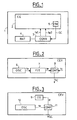
- FIG. 1 represents a portable apparatus 1, which may be, for example, a radiotelephone, essentially comprising a electronic circuit 2, called EC, which is powered by a converter of DC-DC supply voltage 3, called CONV, from a energy source 4 which will classically be a BAT rechargeable battery.
- the CONV converter provides at least one DC supply voltage ta1, but can provide at least a second supply voltage ta2.
- the devices Beside the electronic circuit CE, the devices have not been included human-machine interface, screen, keyboard, etc., that can be found almost always on portable electronic devices and whose power supply poses specific problems that will not be discussed here.
- the electronic circuit CE with the current technique can be realized in the form of an integrated circuit, comprising one or more chips semiconductor material.
- the invention applies regardless of the case.
- evaluation means electronic devices (5) within the electronic circuit CE, arranged to provide an indication sc of the conditions of operation of the electronic circuit CE, which is used to adjust the supply voltage ta 1 to a minimum value that still allows a correct operation of said electronic circuit CE.
- the indication sc is an electrical signal, a voltage for example, which can have two (or more) values, each value prescribing an evolution of the supply voltage ta1 (and ta2). For example, if the signal sc is positive voltage (above a given threshold), the voltage ta 1 must be increased of a given elementary quantity. If the signal sc is negative voltage (below another given threshold), the voltage ta1 must be reduced by one same basic amount. Between the two threshold values mentioned, the signal sc has no influence.
- the signal sc thus makes it possible to adjust the supply voltage.
- the conditions in which it is provided will allow it to be adjusted as indicated above, to a minimum value that still allows a functioning correct of said electronic circuit CE. It is necessary to consider the mode of realization of the CEV electronic evaluation means.
- CEV evaluation are called electronic because they must be sensitive to the same environmental conditions as the EC circuit, and in much the same way, and also be sensitive to the tension feeding, but only in a way that allows the adjustment of the voltage to a minimum value, for example in a loop servo.
- FIG. 2 represents the diagram of a first form of realization of the evaluation means CEV of the apparatus of FIG. which is an oscillator 6, called OSC, providing a signal of frequency fe to a frequency / voltage converter 7, called F / T, which provides an evaluation voltage signal te to a voltage comparator 8, called COMT, which also receives a set voltage tc.
- This COMT comparator provides the sc signal for voltage adjustment as indicated in the description relating to FIG.
- All the circuits of the CEV evaluation facilities should preferably be realized in the same technology as the electronic circuit CE, to have the same behavior, both in the face of environmental conditions and in front of the different values of the supply voltage.
- the circuit This is essentially an integrated circuit, the CEV means are advantageously integrated in the same chip.
- the oscillator OSC can be a simple loop of identical doors, in odd number. Its natural oscillation frequency will depend on the time of transit of a door and will be a representation of the operating conditions of the entire CE circuit.
- the frequency / voltage converter FT can be essentially a Linear integrator integrating amplitude-duration surface impulses constant at the frequency of the signal fe and thus providing a signal of voltage proportional to their frequency.
- the comparator COMT receives this signal te and also a predefined voltage tc, to provide a signal sc equal to the difference tc - te.
- tc predefined voltage
- the comparator COMT receives this signal te and also a predefined voltage tc, to provide a signal sc equal to the difference tc - te.
- FIG. 3 represents in fact a variant of the evaluation means CEV of FIG. 2, in which an oscillator 9, called CO, providing a stable frequency ff, being already available in the electronic circuit CE, the frequency fe of an oscillator OSC 10 is compared with this stable frequency ff in a COMF frequency comparator 11, which directly supplies the signal sc.
- CO oscillator 9
- FIG. 4 represents another embodiment of the means evaluation system of FIG. 1 comprising a stimulus generator 12, referred to as GS, which cyclically provides signal combinations st which are applied to a set of tested circuits 13, called CT, which in response provide rep response signals transmitted to a circuit 14, referred to as CAT, which in return provides the signal sc.
- the stimulus generator GS can be a read memory periodically during rest periods of the EC circuit.
- the signal combinations are applied to tested circuits that are either a subassembly of the CE circuit, a dedicated test circuit comprising circuits switching devices, memories, etc., constituting a representation of the circuit CE, and whose rep answer, ie the signals obtained in exchange for stimuli st, is evaluated, that is, for example, compared to an expected response, to produce a signal sc which is an evaluation of the operation of the EC circuit in accordance with the above Figures 1 to 3.
- FIG. 5 represents one embodiment of the means evaluation of FIG. 1 comprising a measuring device or temperature sensor 15, called DMT, which provides an indication of temperature mt at a temperature response table 16, called TRT, which provides a sd signal.
- DMT measuring device or temperature sensor 15
- TRT temperature response table 16
- Temperature sensors are known to those skilled in the art.
- the temperature measurement mt is a numerical value.
- the TT table is filled in following a test cycle that indicates for each temperature sd of the circuit What should be the supply voltage supplied to the EC circuit.
- the signal sd provides this indication.
- Figure 5 still represents a supply voltage comparator 17, referred to as COMV, which also receives the voltage ta1 and which provides the signal of command sc, under the conditions already discussed above. But he is obvious that the sd signal could be transmitted directly to a power converter such as CONV ( Figure 1), but arranged for respond directly to a signal sd indicating a voltage level supplying a supply voltage ta1, ta2 in response having this level.
- CONV Figure 1
Landscapes
- Engineering & Computer Science (AREA)
- Computer Networks & Wireless Communication (AREA)
- Signal Processing (AREA)
- Mobile Radio Communication Systems (AREA)
- Control Of Voltage And Current In General (AREA)
- Dc-Dc Converters (AREA)
- Power Sources (AREA)
- Direct Current Feeding And Distribution (AREA)
- Measurement Of Current Or Voltage (AREA)
Description
- la figure 1, le diagramme général d'un appareil incorporant la présente invention,
- la figure 2, une première forme de réalisation des moyens d'évaluation de l'appareil de la figure 1,
- la figure 3, une deuxième forme de réalisation des moyens d'évaluation de l'appareil de la figure 1,
- la figure 4, une troisième forme de réalisation des moyens d'évaluation de l'appareil de la figure 1,
- la figure 5, une quatrième forme de réalisation des moyens d'évaluation de l'appareil de la figure 1.
Claims (5)
- Système d'alimentation optimisée pour circuit électronique dont la tension d'alimentation est fournie par un convertisseur de tension continu-continu variable, à partir d'une pile ou d'une batterie rechargeable, caractérisé en ce que des moyens d'évaluation électroniques sont prévus au sein du circuit électronique, de manière à fournir, durant le fonctionnement du circuit électronique, une indication des conditions de fonctionnement du circuit électronique, laquelle est utilisée pour ajuster la tension d'alimentation jusqu'à une valeur minimale qui permette encore un fonctionnement correct dudit circuit électronique.
- Système d'alimentation conforme à la revendication 1, caractérisé en ce que lesdits moyens d'évaluation électroniques comprennent un oscillateur (OSC) dont la fréquence de fonctionnement (fe) fournit ladite indication.
- Système d'alimentation conforme à la revendication 2, caractérisé en ce que ladite fréquence est ensuite convertie en un signal de tension correspondante (te), lequel est comparé à une valeur de consigne (tc) qui est aussi une tension, le résultat de ladite comparaison (sc) étant utilisé pour ajuster la tension d'alimentation (ta1) jusqu'à une valeur minimale qui permette encore un fonctionnement correct dudit circuit électronique.
- Système d'alimentation conforme à la revendication 1, caractérisé en ce que lesdits moyens d'évaluation (CEV) comprennent un circuit de test (CT) comprenant au moins un circuit sensible à la valeur de la tension d'alimentation et aux conditions d'environnement, recevant périodiquement un ou des stimuli (st) et fournissant au moins une réponse (rep) utilisée pour ajuster la tension d'alimentation jusqu'à une valeur minimale qui permette encore un fonctionnement correct dudit circuit électronique.
- Système d'alimentation conforme à la revendication 1, caractérisé en ce que lesdits moyens d'évaluation (CEV) comprennent un dispositif DT) fournissant un signal d'évaluation représentant la température à laquelle est soumis ledit circuit électronique (CE) et un dispositif de conversion (TRT) traduisant ledit signal d'évaluation en un signal de commande (sd, sc) utilisé pour ajuster la tension d'alimentation jusqu'à une valeur minimale qui permette encore un fonctionnement correct dudit circuit électronique.
Applications Claiming Priority (2)
| Application Number | Priority Date | Filing Date | Title |
|---|---|---|---|
| FR9801334 | 1998-02-05 | ||
| FR9801334A FR2774487B1 (fr) | 1998-02-05 | 1998-02-05 | Systeme d'alimentation optimisee pour circuit electronique |
Publications (2)
| Publication Number | Publication Date |
|---|---|
| EP0935399A1 EP0935399A1 (fr) | 1999-08-11 |
| EP0935399B1 true EP0935399B1 (fr) | 2005-10-05 |
Family
ID=9522620
Family Applications (1)
| Application Number | Title | Priority Date | Filing Date |
|---|---|---|---|
| EP99400131A Expired - Lifetime EP0935399B1 (fr) | 1998-02-05 | 1999-01-21 | Système d'alimentation optimisée pour circuit électronique |
Country Status (6)
| Country | Link |
|---|---|
| US (1) | US6366072B2 (fr) |
| EP (1) | EP0935399B1 (fr) |
| JP (1) | JP4230586B2 (fr) |
| CA (1) | CA2259479A1 (fr) |
| DE (1) | DE69927537T2 (fr) |
| FR (1) | FR2774487B1 (fr) |
Families Citing this family (8)
| Publication number | Priority date | Publication date | Assignee | Title |
|---|---|---|---|---|
| US20060174303A1 (en) * | 2003-04-15 | 2006-08-03 | Kanazawa University Technology Licensing Organization Ltd. | Moving picture encoding or decoding processing system and mobin g picture encoding or decoding processing method |
| US7886167B2 (en) * | 2006-05-11 | 2011-02-08 | Intel Corporation | Load circuit supply voltage control |
| FR2964512B1 (fr) * | 2010-09-02 | 2013-06-28 | Finsecur | Dispositif electronique autonome a consommation d'energie reduite et procede d'economie d'energie |
| US10209726B2 (en) | 2016-06-10 | 2019-02-19 | Microsoft Technology Licensing, Llc | Secure input voltage adjustment in processing devices |
| US10310572B2 (en) | 2016-06-10 | 2019-06-04 | Microsoft Technology Licensing, Llc | Voltage based thermal control of processing device |
| US10338670B2 (en) | 2016-06-10 | 2019-07-02 | Microsoft Technology Licensing, Llc | Input voltage reduction for processing devices |
| US10248186B2 (en) | 2016-06-10 | 2019-04-02 | Microsoft Technology Licensing, Llc | Processor device voltage characterization |
| CN112448396B (zh) * | 2020-11-17 | 2023-11-10 | 海南省电力学校(海南省电力技工学校) | 一种虚拟电厂自趋优负荷跟踪控制方法 |
Family Cites Families (25)
| Publication number | Priority date | Publication date | Assignee | Title |
|---|---|---|---|---|
| JPS5596339A (en) * | 1979-01-13 | 1980-07-22 | Nippon Denso Co Ltd | Air-fuel ratio control method |
| JPS593635Y2 (ja) * | 1979-09-29 | 1984-02-01 | 日本電気株式会社 | 選択呼出受信機 |
| JPS5652440U (fr) * | 1979-09-29 | 1981-05-09 | ||
| DE3063190D1 (en) * | 1980-01-17 | 1983-06-16 | Autophon Ag | Portable paging receiver with a shift register and a direct current converter |
| GB2132452B (en) * | 1982-12-08 | 1986-10-08 | Racel Ses Limited | Radio systems |
| US4495648A (en) * | 1982-12-27 | 1985-01-22 | At&T Bell Laboratories | Transmitter power control circuit |
| JPS60145735A (ja) * | 1984-01-09 | 1985-08-01 | Nec Corp | バツテリ−セ−ビング方式 |
| JPS60170344A (ja) * | 1984-02-14 | 1985-09-03 | Matsushita Electric Ind Co Ltd | 選択呼出受信装置 |
| IT1227731B (it) * | 1988-12-28 | 1991-05-06 | Sgs Thomson Microelectronics | Stabilizzatore di tensione a bassissima caduta di tensione, atto a sopportare transitori di tensione elevata |
| US5218705A (en) * | 1989-04-17 | 1993-06-08 | Motorola, Inc. | Pager receiver with selective operating voltage and reduced power consumption |
| US5153535A (en) * | 1989-06-30 | 1992-10-06 | Poget Computer Corporation | Power supply and oscillator for a computer system providing automatic selection of supply voltage and frequency |
| US5606739A (en) * | 1991-04-19 | 1997-02-25 | Kabushiki Kaisha Toshiba | Radio communication apparatus having a battery saving function |
| US5285850A (en) * | 1991-10-11 | 1994-02-15 | Halliburton Company | Well completion system for oil and gas wells |
| US5191278A (en) * | 1991-10-23 | 1993-03-02 | International Business Machines Corporation | High bandwidth low dropout linear regulator |
| US5384564A (en) * | 1992-01-23 | 1995-01-24 | Keith H. Wycoff | Battery saving arrangement for selectively addressable, portable receivers |
| US5625278A (en) * | 1993-06-02 | 1997-04-29 | Texas Instruments Incorporated | Ultra-low drop-out monolithic voltage regulator |
| US5285650A (en) * | 1993-07-27 | 1994-02-15 | Lin Che Tzu | Automobile condenser electric fan controller |
| US5629609A (en) * | 1994-03-08 | 1997-05-13 | Texas Instruments Incorporated | Method and apparatus for improving the drop-out voltage in a low drop out voltage regulator |
| JPH0847251A (ja) * | 1994-07-29 | 1996-02-16 | Internatl Business Mach Corp <Ibm> | スイッチング・レギュレータ、情報処理装置及びその制御方法 |
| JP3047345B2 (ja) * | 1995-04-28 | 2000-05-29 | 静岡日本電気株式会社 | バッテリーセービング機能付き選択呼出受信機 |
| US5686821A (en) * | 1996-05-09 | 1997-11-11 | Analog Devices, Inc. | Stable low dropout voltage regulator controller |
| US5760636A (en) * | 1996-06-28 | 1998-06-02 | Intel Corporation | Adjusting clock frequency and voltage supplied to a processor in a computer system |
| DE59701197D1 (de) * | 1996-09-18 | 2000-04-06 | Siemens Ag | Verfahren und schaltungsanordnung zur spannungsversorgung in elektrischen funktionseinheiten |
| US5864225A (en) * | 1997-06-04 | 1999-01-26 | Fairchild Semiconductor Corporation | Dual adjustable voltage regulators |
| US5977733A (en) * | 1998-12-08 | 1999-11-02 | Shin Jiuh Corporation | Fan control device with breakdown warning capability |
-
1998
- 1998-02-05 FR FR9801334A patent/FR2774487B1/fr not_active Expired - Fee Related
-
1999
- 1999-01-21 DE DE69927537T patent/DE69927537T2/de not_active Expired - Lifetime
- 1999-01-21 EP EP99400131A patent/EP0935399B1/fr not_active Expired - Lifetime
- 1999-02-03 CA CA002259479A patent/CA2259479A1/fr not_active Abandoned
- 1999-02-04 US US09/244,827 patent/US6366072B2/en not_active Expired - Lifetime
- 1999-02-04 JP JP02790099A patent/JP4230586B2/ja not_active Expired - Fee Related
Also Published As
| Publication number | Publication date |
|---|---|
| US6366072B2 (en) | 2002-04-02 |
| US20020007262A1 (en) | 2002-01-17 |
| FR2774487A1 (fr) | 1999-08-06 |
| DE69927537T2 (de) | 2006-07-13 |
| FR2774487B1 (fr) | 2000-09-29 |
| EP0935399A1 (fr) | 1999-08-11 |
| JPH11332093A (ja) | 1999-11-30 |
| DE69927537D1 (de) | 2005-11-10 |
| CA2259479A1 (fr) | 1999-08-05 |
| JP4230586B2 (ja) | 2009-02-25 |
Similar Documents
| Publication | Publication Date | Title |
|---|---|---|
| EP0407268B1 (fr) | Circuit intégré à microprocesseur et horloge interne programmable | |
| EP0110775A1 (fr) | Régulateur à faible tension de déchet | |
| US6476587B2 (en) | Power circuit, power circuit control method and electronic device using the power circuit | |
| EP0935399A1 (fr) | Système d'alimentation optimisée pour circuit électronique | |
| WO2003052567A3 (fr) | Dispositif flash fonctionnant a partir d'une alimentation electrique en boitier ou d'une alimentation electrique sur puce | |
| CN111655534B (zh) | 用于估计soc的装置和方法 | |
| US6646960B1 (en) | Electronic timepiece | |
| US5847794A (en) | Photovoltaic module with display indicator | |
| JP2524911B2 (ja) | 充電装置 | |
| FR2605153A1 (fr) | Systeme autonome d'alimentation electrique | |
| Huet et al. | Design strategy of conventional electronic for wireless sensor node powered by vibration energy harvester | |
| JP2001133539A (ja) | レーダ探知システム | |
| JP2565018Y2 (ja) | 電源回路 | |
| JPH09264971A (ja) | 電力制御装置、発電装置および電子機器 | |
| US20250358371A1 (en) | Power sharing for smart doorbell head and chime controller | |
| CN214380266U (zh) | 电池控制装置、储能电源及其储能系统 | |
| EP0704800A3 (fr) | Dispositif de mémoire à semi-conducteur avec circuit de génération d'un signal de sélection d'une ligne de données redondante | |
| JPH01308135A (ja) | 車両用発電制御装置 | |
| US4530581A (en) | Information display device for camera | |
| EP3510682A1 (fr) | Circuit de transmission d'énergie électrique | |
| JPS5815440U (ja) | 充電回路 | |
| JP3675060B2 (ja) | 電力供給装置、発電装置および電子機器 | |
| US6029014A (en) | Light measuring apparatus and camera using the light measuring apparatus | |
| JP2934891B2 (ja) | カメラ用モータ駆動装置 | |
| JPH0669272B2 (ja) | 太陽光発電装置の負荷制御方式 |
Legal Events
| Date | Code | Title | Description |
|---|---|---|---|
| PUAI | Public reference made under article 153(3) epc to a published international application that has entered the european phase |
Free format text: ORIGINAL CODE: 0009012 |
|
| AK | Designated contracting states |
Kind code of ref document: A1 Designated state(s): DE ES GB IT |
|
| AX | Request for extension of the european patent |
Free format text: AL;LT;LV;MK;RO;SI |
|
| 17P | Request for examination filed |
Effective date: 20000211 |
|
| AKX | Designation fees paid |
Free format text: DE ES GB IT |
|
| 17Q | First examination report despatched |
Effective date: 20040220 |
|
| GRAP | Despatch of communication of intention to grant a patent |
Free format text: ORIGINAL CODE: EPIDOSNIGR1 |
|
| GRAS | Grant fee paid |
Free format text: ORIGINAL CODE: EPIDOSNIGR3 |
|
| GRAA | (expected) grant |
Free format text: ORIGINAL CODE: 0009210 |
|
| AK | Designated contracting states |
Kind code of ref document: B1 Designated state(s): DE ES GB IT |
|
| REG | Reference to a national code |
Ref country code: GB Ref legal event code: FG4D Free format text: NOT ENGLISH |
|
| REF | Corresponds to: |
Ref document number: 69927537 Country of ref document: DE Date of ref document: 20051110 Kind code of ref document: P |
|
| GBT | Gb: translation of ep patent filed (gb section 77(6)(a)/1977) | ||
| PG25 | Lapsed in a contracting state [announced via postgrant information from national office to epo] |
Ref country code: ES Free format text: LAPSE BECAUSE OF FAILURE TO SUBMIT A TRANSLATION OF THE DESCRIPTION OR TO PAY THE FEE WITHIN THE PRESCRIBED TIME-LIMIT Effective date: 20060116 |
|
| PLBE | No opposition filed within time limit |
Free format text: ORIGINAL CODE: 0009261 |
|
| STAA | Information on the status of an ep patent application or granted ep patent |
Free format text: STATUS: NO OPPOSITION FILED WITHIN TIME LIMIT |
|
| 26N | No opposition filed |
Effective date: 20060706 |
|
| REG | Reference to a national code |
Ref country code: GB Ref legal event code: 732E Free format text: REGISTERED BETWEEN 20131114 AND 20131120 |
|
| PGFP | Annual fee paid to national office [announced via postgrant information from national office to epo] |
Ref country code: DE Payment date: 20160120 Year of fee payment: 18 Ref country code: IT Payment date: 20160127 Year of fee payment: 18 |
|
| PGFP | Annual fee paid to national office [announced via postgrant information from national office to epo] |
Ref country code: GB Payment date: 20160120 Year of fee payment: 18 |
|
| REG | Reference to a national code |
Ref country code: DE Ref legal event code: R119 Ref document number: 69927537 Country of ref document: DE |
|
| GBPC | Gb: european patent ceased through non-payment of renewal fee |
Effective date: 20170121 |
|
| PG25 | Lapsed in a contracting state [announced via postgrant information from national office to epo] |
Ref country code: GB Free format text: LAPSE BECAUSE OF NON-PAYMENT OF DUE FEES Effective date: 20170121 Ref country code: DE Free format text: LAPSE BECAUSE OF NON-PAYMENT OF DUE FEES Effective date: 20170801 |
|
| PG25 | Lapsed in a contracting state [announced via postgrant information from national office to epo] |
Ref country code: IT Free format text: LAPSE BECAUSE OF NON-PAYMENT OF DUE FEES Effective date: 20170121 |