EP0933902A2 - Démodulation avec compensation d'évanouissements - Google Patents
Démodulation avec compensation d'évanouissements Download PDFInfo
- Publication number
- EP0933902A2 EP0933902A2 EP99300466A EP99300466A EP0933902A2 EP 0933902 A2 EP0933902 A2 EP 0933902A2 EP 99300466 A EP99300466 A EP 99300466A EP 99300466 A EP99300466 A EP 99300466A EP 0933902 A2 EP0933902 A2 EP 0933902A2
- Authority
- EP
- European Patent Office
- Prior art keywords
- signal
- fading distortion
- estimated
- output
- fading
- Prior art date
- Legal status (The legal status is an assumption and is not a legal conclusion. Google has not performed a legal analysis and makes no representation as to the accuracy of the status listed.)
- Granted
Links
Images


Classifications
-
- H—ELECTRICITY
- H04—ELECTRIC COMMUNICATION TECHNIQUE
- H04B—TRANSMISSION
- H04B7/00—Radio transmission systems, i.e. using radiation field
- H04B7/005—Control of transmission; Equalising
-
- H—ELECTRICITY
- H04—ELECTRIC COMMUNICATION TECHNIQUE
- H04L—TRANSMISSION OF DIGITAL INFORMATION, e.g. TELEGRAPHIC COMMUNICATION
- H04L27/00—Modulated-carrier systems
- H04L27/18—Phase-modulated carrier systems, i.e. using phase-shift keying
- H04L27/22—Demodulator circuits; Receiver circuits
- H04L27/233—Demodulator circuits; Receiver circuits using non-coherent demodulation
- H04L27/2332—Demodulator circuits; Receiver circuits using non-coherent demodulation using a non-coherent carrier
Definitions
- the present invention relates to digital modulation/demodulation used for satellite communication, mobile communication, mobile satellite communication, in particular, to a demodulator periodically inserting a known signal into transmitted signals, estimating channel distortion from the known signal, eliminating the channel distortion using the estimated value, and performing coherent detection of the received signal.
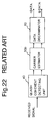
- Figs. 22 and 23 show conventional demodulation circuits disclosed in, for example, "Rayleigh Fading Compensation Method for 16QAM MODEM in Digital Land Mobile Radio Systems” (Sampei, Theses of The Institute of Electronics, Information and Communication Engineers (B-II), J72-II, No. 1, pp7 - 15 (1989-1)).
- a reference numeral 40 shows a quasicoherent detecting unit
- a reference numeral 50p shows a carrier estimator
- 60 shows a data discriminator.
- a reference numeral 51 shows a fading distortion estimator and 52 shows a fading distortion compensator.
- a transmitted signal S T (t), modulated by QPSK is given by the following expression (1).
- the faded signal is represented by a narrow-band random complex signal c(t) having fading power spectrum S(f) multiplied to S T (t).
- the received signal S R (t) faded by an envelope variation c(t) is given by expression (3).
- s R ( t ) Re[ c ( t ) z R ( t )exp( j 2 ⁇ f c t ) + n ( t )exp( j 2 ⁇ f c t )]
- z R (t) denotes the received baseband complex signal limited by the transmitter and receiver filters.
- n(t) denotes a white Gaussian noise.
- the quasi-coherent detection is performed on the received signal by the quasi-coherent detecting unit 40 with a local oscillator having oscillating frequency of f c - f off .
- a signal S RB (t) output from the quasi-coherent detecting unit 40 is given by the following expression (4).
- the carrier estimator 50p obtains c R (t), the estimation value of c(t) from the baseband signal u(t) output from the quasi-coherent detecting unit 40.
- the carrier estimator 50p also eliminates the distortion caused by c(t) from the received signal.
- c R (t) the estimation value of c(t) is obtained by the expression (6).
- u ( t ) c ( t ) a p + n ( t )
- An estimation of an interpolation sequence c RI (t) out of c RS (t) is, for example, performed by the following way using the interpolation.
- the fading compensator 52 eliminates the fading distortion from the received signal using the interpolation sequence c RI (k+m/N R ) output from the fading distortion estimator 51.
- a transmission function h(k+m/N R ) for compensating the fading distortion is represented by the following expression (9).
- the received signal z RE (k+m/N R ) of which fading distortion was compensated, can be obtained.
- the fading distortion of the information signal is estimated by the interpolation using the estimation value of the fading distortion obtained by the known signal. Therefore, in the nonfading channel or Rician fading channel, where thermal noise influences a lot in addition to the fading variation, an error of the estimation value obtained by the known signal becomes large, the fading distortion cannot be compensated properly, which degrades performance of the receiver such as a bit error rate characteristic.
- the fading channel and the nonfading channel have opposite characteristics, so that when the performance of the receiver is improved in one of two above channels, the performance of the receiver is degraded in the other channel. It is difficult to embody the receiver having a high performance in wide range from the fading channel to nonfading channel.
- the present invention is provided to solve the abovementioned problems.
- the invention aims to have a demodulator, where the estimation error of the fading distortion is reduced to improve the receiving performance such as the bit error rate characteristic not only in the fading channel, but also in a channel where the thermal noise influences a lot in addition to the fading variation such as the nonfading channel and Rician fading channel, or, in the fading channel where C/N rate is low, the estimation error of the fading distortion is made small to improve the receiving performance such as the bit error rate characteristic.
- a demodulator for estimating a carrier, and for coherent detection using specific symbols inserted in received signals has a fading distortion estimator and a fading distortion compensator using an output of the fading distortion estimator.
- the demodulator includes:
- a demodulation method in a demodulator having a fading distortion estimator and a fading distortion compensator using an output of the fading distortion estimator includes:
- a demodulator which performs coherent detection with compensating an amplitude and a phase of the received signal using a reference signal generated by complex multiplying an average value of the distortion compensated signal to the estimated fading distortion.
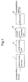
- Fig. 1 shows a configurational example of a transmitter of the first embodiment performing coherent detection of the received signal using a known signal inserted into transmitted signals.
- a reference numeral 1 shows a convolutional encoder
- 10 shows an interleaving unit
- 20 shows a known signal inserting unit
- 30 shows a modulator.
- the convolutional encoder 1 implements convolutional encoding to an information signal and output the code.
- the interleaving unit 10 arranges the encoded data supplied from the convolutional encoder 1 according to a specific rule.
- the known signal inserting unit 20 periodically inserts a known signal into the data output from the interleaving unit 10 and output the data.
- the signal output from the known signal inserting unit 20 becomes, for example, as shown in Fig. 2, the information signal of (N R -R) symbols periodically inserted the known signal of R symbol.
- the modulator 30 modulates the signal supplied from the known signal inserting unit 20 and outputs the modulated signal as a transmitting signal.
- the transmitting signal is, for example, modulated by QPSK modulating system and transmitted.
- Fig. 3 shows a configurational example of the receiver of the first embodiment performing coherent detection of the received signal using the known signal inserted into the transmitted signals.
- a reference numeral 40 shows a quasi-coherent detecting unit
- 50 shows a carrier estimator
- 60 shows a data discriminator
- 70 shows a di-interleaving unit
- 80 shows a Viterbi decoder.
- the quasi-coherent detecting unit 40 converts the frequency of the RF/IF (Radio Frequency/Intermediate Frequency) signal by orthogonal detection.
- the converted signal is further sampled by the A/D (analog to digital) converter to the discrete value, and is output as baseband signals of I channel and Q channel.
- the carrier estimator 50 obtains the estimated value c R (t) of the fading distortion c(t) to eliminate the distortion of the signal caused by fading, etc. from the baseband signals of I channel and Q channel.
- the data discriminator 60 discriminates the transmitted signal from the baseband signals in the I channel and Q channel, which was performed coherent detection and supplied from the carrier estimator 50.
- the diinterleaving unit 70 rearranges the data, which was arranged by the interleaving unit 20 according to the specific rule, to the original order.
- the Viterbi decoder 80 decodes the data supplied from the di-interleaving unit 70 using Viterbi algorithm.
- Fig. 4 shows a configurational example of the carrier estimator performing coherent detection of the received signal using the known signal inserted into the transmitted signals.
- a reference numeral 51 shows a fading distortion estimator
- 52 shows a fading distortion compensator
- 53 shows a modulation component eliminator
- 54 shows an averaging unit
- 55 shows an estimated signal generator
- 56 shows a signal compensator.
- the fading distortion estimator 51 estimates the fading distortion of the information signal using the known signal periodically inserted into the transmitted signals.
- the fading distortion compensator 52 compensates the fading distortion using the estimated value of fading distortion obtained by the fading distortion estimator 51, and eliminates the fading distortion from the signal output from the quasi-coherent detecting unit 40.
- the fading distortion estimator 51 and the fading distortion compensator 52 operate, for example, as described in the conventional related art.
- the fading distortion compensator 52 eliminates the fading distortion from the received signal using the interpolation sequence c RI (k+m/N R ) supplied from the fading distortion estimator 51. Namely, a transfer function h(k+m/N R ) for compensating the fading distortion is given by the following expression (12).
- the fading distortion can be compensated as given by the following expression (13) from the signal supplied from the quasi-coherent detecting unit 40.
- the modulation component eliminator 53 eliminates the modulation component from the received signal z RE (k+mN R ), which was compensated fading distortion and supplied from the fading distortion compensator 52. For example, assuming QPSK modulation signal having four phases of 45°, 135°, 225°, and 315° as signal points, the above elimination corresponds reducing the signal having the first quadrant through the fourth quadrant to only the first quadrant.
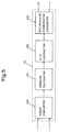
- Fig. 5 shows a configurational example of the modulation component 53.
- a reference numeral 530 shows an angle converter
- 531 shows a residual calculator
- 532 shows a ⁇ /4 subtractor
- 533 shows a orthogonal coordinates converter.
- the angle converter 530 converts the angles of I data and crossed Q data so as to be phase data.
- the residual calculator 531 divides the phase data output from the angle converter 530 by 90° and outputs the residue of the division.
- the ⁇ /4 subtractor 532 subtracts 45° from the phase data output from the residual calculator 531.
- the orthogonal coordinates converter 533 converts the phase data output from the ⁇ /4 subtractor 532 into rectangular coordinates. This operation can be represented by the following expression (14), where the phase component of z RE (k+m/N R ) is assumed to be ⁇ RE (k+m/N R ) and the signal eliminated by the modulation component eliminator 53 is assumed to be z RF (k+m/N R ).
- Re[ ⁇ ] represents a real part of [ ⁇ ]
- Im[ ⁇ ] represents an imaginary part of [ ⁇ ].
- the averaging unit 54 performs moving average of the signal of which the modulation component was eliminated by the modulation component eliminator 53 and compensated fading distortion.
- Fig. 6 shows a configurational example of the averaging unit 54.
- a reference numeral 540 shows an N-stage shift register, and 541 shows an adder.
- the adder 541 performs addition to each symbol of N pieces of data stored in the N-stage shift register 540, and outputs the result of the addition. This operation will be represented by the following expression (15).
- the estimated signal generator 55 compounds the estimated value c RI (k+m/N R ) of the fading distortion obtained by the fading distortion estimator 51 and the mean value z AV (k+m/N R ) output from the averaging unit 54, and generates a reference signal for estimating the carrier phase and performing coherent detection.
- Fig. 7 shows a concept of the estimated signal generator 55.
- a reference numeral 550 shows a complex multiplier.
- the complex multiplier 550 multiplies the signal output from the averaging unit 54 to the signal output from the fading distortion estimator 51 and outputs the result of the multiplication.
- This operation equals to the following expression (16) compounding and outputting the reference signal c EST (k+m/N R ) for coherent detection.
- c EST k + m N R c RI k + m N R ⁇ z AV k + m N R
- the estimated signal generator compounds a signal as given by the following expression and outputs the reference signal c EST (K+m/N R ) .
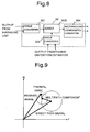
- Fig. 8 shows a configurational example of the estimated signal generator 55.
- a reference numerals 551 and 552 show angle converters
- 553 shows an adder
- 554 shows an orthogonal coordinates converter.
- the angle converter 551 converts the signal output from the averaging unit 54 into the phase data.
- the angle converter 552 converts the signal output from the fading distortion estimator 51 into the phase data.
- the adder 553 adds the phase data output from the angle converter 551 and the phase data output from the angle converter 552.
- the orthogonal coordinates converter 554 converts the phase data output from the adder 553 into the rectangle coordinates, and outputs I data and Q data. This operation equals to the following expression (17) generating the signal and outputting the reference signal c EST (k+m/N R ) for coherent detection.
- the signal compensator 56 compensates the amplitude and the phase of the received signal using the reference signal c EST (k+m/N R ) output from the estimated signal generator 55 and performs coherent detection.
- the received signal z RC (k+m/N R ) of the following expression (18) is obtained.
- Fig. 9 shows a signal vector diagram of the received signal, where the channel is assumed to be Rician fading channel.
- a signal vector is configured by the direct path. signal and multipath component. Further, the thermal noise generated in the receiver is added to the faded signal.
- the fading distortion estimator 51 mainly estimates the fading distortion based on the signal compounding the direct path signal and the multipath component, and the fading distortion compensator 52 compensates the fading distortion.
- the averaging unit 54 estimates distortion of the signal mainly caused by the thermal noise, which was not sufficiently compensated by the fading distortion compensator 52. By compounding the estimated values obtained by the fading distortion estimator 51 and by the averaging unit 54, both signal distortion caused by the fading and by the thermal noise can be estimated and compensated to be performed coherent detection.
- the signal is averaged to detect the estimation error caused by the thermal noise.
- the obtained estimation error is compounded to the estimated value supplied from the fading distortion estimator to obtain the reference signal to compensate the received signal.
- the estimation error caused by the thermal noise which was not sufficiently compensated, can be detected and the degradation of the characteristic caused by the fading and the thermal noise can be reduced.
- the signal is supposed to be modulated by the QPSK modulation method.
- the demodulator of the embodiment includes the convolutional encoder, the Viterbi decoder, the interleaving unit, and di-interleaving unit, however, these elements are not always required to be included in the demodulator.
- the demodulator having a simpler configuration than the first embodiment, which can reduce the influence of the thermal noise and can be applied to wide range of the characteristic of the channels, will be explained.
- the distortion is not obtained at once, but the distortion of the signal is compensated and then the distortion compensated signal is averaged by each calculation.
- the reference signal can be obtained as a result of this averaging.
- the operation from the coherent detection using the reference signal is the same as the first embodiment.
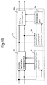
- Fig. 10 shows a configurational example of the carrier estimator 50b performing coherent detection of the received signal using the reference signal inserted into the transmitted signals.
- a reference numeral 51 shows the fading distortion estimator
- 52 shows the fading distortion compensator
- 53 shows the modulation component eliminator
- 54 shows the averaging unit
- 56b shows the signal compensator.
- the fading distortion estimator 51 estimates the fading variation in the information signal using the known signal periodically inserted into the received signal.
- the fading distortion compensator 52 compensates the fading distortion using the fading distortion estimated value estimated by the fading distortion estimator 51, and eliminates the fading distortion from the signal output from the quasi-coherent detector.
- the modulation component eliminator 53 eliminates the modulation component from the signal output from the fading distortion compensator 52.
- the averaging unit 54 averages the signal, of which the modulation component was eliminated by the modulation component eliminator 53 and of which the fading distortion was compensated. These operation are processed, for example, in the way as described in the first embodiment.
- the estimated signal generator is removed.
- the signal compensator 56b compensates the signal output from the fading distortion estimator 52 using the signal output from the averaging unit 54. Namely, when the output from the fading distortion estimator 52 is z RE (k+m/N R ) and the output from the averaging unit 54 is z AV (k+m/N R ) , the received signal z RC (k+m/N R ) of which the carrier phase was compensated, is given by the following expression (19) when the outputs are compounded to generate a signal intruding the amplitude.
- the signal can be compensated in another way as represented by the following expression (20).
- z RC k + m N R z RE k + m N R z AV k + m N R
- the demodulator of the second embodiment first compensates the fading distortion using the known signal, then averages the signal to detect the estimation error due to the thermal noise, and the signal is compensated.
- the embodiment enables to obtain the demodulator detecting the estimation error due to the thermal noise, which was not sufficiently compensated by the fading distortion compensator, and having a simpler configuration than the first embodiment. Accordingly, the demodulator can reduce the degradation of the performance caused by the fading and the thermal noise.
- the fading distortion is estimated not only using the distortion at the location of the known signal, but adding and averaging the signal after weighting the distortion of the previous signal and the subsequent signal. In this way, the distortion can be estimated based on the fading variation with reducing the estimation error due to the thermal noise.
- the carrier estimator performs the coherent detection of the received signal using the known signal inserted into the transmitted signals.
- the fading distortion estimator 51b is configured as shown in Fig. 11. Except the configuration of the fading distortion estimator 51b, the demodulator of the third embodiment has the same configuration of the first embodiment as shown in Fig. 4, or of the second embodiment as shown in Fig. 10.
- a reference numeral 510 shows a known signal extractor
- 511 shows a distortion detecting and averaging unit
- 512 shows a weighted averaging unit
- 513 shows an interpolator.
- the fading distortion estimated value c RB (k) of the known signal having consecutive R symbols is required to be obtained.
- the known signal extractor 510 extracts the signal corresponding to the known signal.
- the extracted known signal having consecutive R symbols is called as a known signal block.
- T R shows an insertion interval of the known signal
- N R shows the number of symbols corresponding to the interval.
- the estimated value c RB (k) of the fading distortion in the known signal block is obtained using the estimated values c R (k), c R (k+1/N R ) of the fading distortion in each known signal, which is given by the following expression (23).
- c RB ( k ) 1 2 ⁇ c R ( k )+ c R k + 1 N R
- the weighted averaging unit 512 performs the weighted average of the estimated value c RB (k) of the fading distortion output from the distortion detecting and averaging unit 511 as shown in the following expression (24).
- K represents a variable deciding the number of known signal blocks for weighted averaging.
- the estimated values of fading distortion in the previous and subsequent known signal blocks are weighted and added. The added result becomes the estimated value of the fading distortion at that location.
- the interpolator 513 estimates the fading distortion c RI (k+m/N R ) in the information signal using the estimated value c RBA (k) of the fading distortion at the known signal location output from the weighted averaging unit 512.
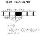
- the conventional way of the interpolation as shown in Fig. 24 can be applied to the above estimation of the fading distortion c RI (k+m/N R ) in the information signal using the estimated value of fading distortion c RBA (k).
- the estimated value c RI (k+m/N R ) of fading distortion in the information signal can be also obtained by, for example, the second order Gaussian interpolation, and the estimated value can be represented by the following expression (25).
- the estimated value c RI (k+m/N R ) of the fading distortion in the information signal, and the estimated value can be represented by the following expression (26).
- X t represents the transposed matrix X.
- the estimated value c RI (k+m/N R ) of the fading distortion in the information signal can be represented by the following expression (27).
- ⁇ represents a correlation function, which can be given by a time correlation function as obtained by the following expression (28), considering the fading process.
- C c RBA ( k -1) c RBA ( k ) c RBA ( k +1)
- H h 0 ( t m ) h 1 ( t m ) h 2 ( t m )
- R r 11 r 21 r 31 r 12 r 22 r 32 r 13 r 23 r 33
- W w m 1 w m 2 w m 3
- R ⁇ ij
- + (dagger) represents a conjugated transposition
- a p represents the known signal
- ⁇ c 2 represents dispersion of the amplitude of received signal
- J O ( ⁇ ) represents the zero-order Bessel function of the first kind
- f D T S represents normalized maximum Doppler frequency
- ⁇ ij represents Kronecker's delta.
- the demodulator of the embodiment averages the estimated value of the fading distortion obtained by the known signal block by adding weighted value to the previous and subsequent signal blocks of the known signal block, and then the interpolation is implemented to estimate the fading distortion.
- the embodiment can reduce the estimation error at the known signal location due to the thermal noise, and degradation of the characteristic caused by the thermal noise with following the fading variation.
- the value of the weighted coefficient is assumed as given by the expression (24).
- the weighted coefficient can be set independently.
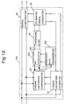
- Fig. 12 shows a configuration of another carrier estimator of the first embodiment performing the coherent detection of the received signal using the known signal inserted into the transmitted signals.
- the modulation component eliminator of the first embodiment is now configured as shown in Fig. 12.
- a reference numeral 534 shows a temporary data discriminator
- 535 shows a re-modulator.
- the other elements of the configuration of Fig. 12 are the same as elements of the first embodiment shown in Fig. 4. These are assigned the same reference numerals, and the explanation of the numerals are omitted.
- the temporary data discriminator 534 temporarily discriminates the transmitted signal from the output signal of the fading distortion compensator 52.
- the re-modulator 535 eliminates the modulation component by re-modulating the signal using the decoded data discriminated and output by the temporary data discriminator 534. This operation is represented by the following expression (29), where the output of the fading distortion compensator 52 is z RE (k+m/N R ) , and the signal of which the modulation component is eliminated is z RF (k+m/N R ) .
- Int[ ⁇ ] means to convert into an integral value by cutting off the decimal part.
- the modulation component is eliminated by re-modulating the signal using the output from the temporary data discriminator. Since the carrier estimator of the present embodiment can eliminate the modulation component more precisely than eliminating the modulation component by Nth power law and so on, which reduces the estimation error generated by the averaging unit, and the performance of the receiver has been improved. Further, the number of stages required for averaging to obtain the same performance can be decreased, thus the load of the averaging unit can be lessened.
- Fig. 13 shows a configuration of another carrier estimator of the second embodiment, which performs coherent detection of the received signal using the known signal inserted into the transmitted signals.
- the modulation component eliminator of the second embodiment is now configurated as shown in Fig. 13.
- a reference numeral 534d shows a temporary data discriminator
- 535d shows a re-modulator
- the temporary data discriminator 534d temporarily discriminates the transmitted data from the output signal of the fading distortion compensator 52.
- the re-modulator 535d eliminates the modulation component by re-modulating the signal using the decoded data discriminated and output by the temporary data discriminator 534d. These operation are performed in the same way as, for example, the demodulator of the fourth embodiment configured as shown Fig. 12.
- the modulation component is eliminated by re-modulating the signal using the output from the temporary data discriminator. Since the carrier estimator of the present embodiment can eliminate the modulation component more precisely than Nth power law and so on, which reduces the estimation error generated by the averaging unit, and the performance of the receiver has been improved. Further, the number of stages required for averaging can be decreased, thus the load of the averaging unit can be lessened.
- Fig. 14 shows a configuration of another carrier estimator of the first embodiment performing the coherent detection of the received signal using the known signal inserted into the transmitted signals.
- the modulation component eliminator of the first embodiment is now configured as shown in Fig. 14.
- a reference numeral 534e shows a temporary data discriminator
- 535e shows a re-modulator
- the temporary data discriminator 534e temporarily discriminates the transmitted signal from the output signal of the signal compensator 56.
- the re-modulator 535e eliminates the modulation component by remodulating the signal using the decoded data discriminated and output by the temporary data discriminator 534e. This operation is represented by the following expression (30), where the output of the signal compensator 56 is z RC (k+m/N R ) , and the signal of which the modulation component is eliminated is z RF (k+m/N R ) .
- the modulation component is eliminated by remodulating the signal using the output from the temporary data discriminator, which enables the carrier estimator of the present embodiment to eliminate the modulation component more precisely than the fourth embodiment. Accordingly, the estimation error generated by the averaging unit can be reduced, and the performance of the receiver is improved. Further, the number of stages required for averaging to obtain the same performance can be decreased, thus the load of the averaging unit can be lessened.
- Fig. 15 shows a configuration of another carrier estimator of the second embodiment, which performs the coherent detection of the received signal using the known signal inserted into the transmitted signals.
- the modulation component eliminator of the second embodiment is now configurated as shown in Fig. 15.
- a reference numeral 534f shows a temporary data discriminator
- 535f shows a re-modulator
- the temporary data discriminator 534f temporarily discriminates the transmitting data from the output signal of the signal compensator 56.
- the re-modulator 535f eliminates the modulation component by remodulating the signal using the decoded data discriminated and output by the temporary data discriminator 534f.
- the modulation component is eliminated by remodulating the signal using the output from the temporary data discriminator, which enables the carrier estimator of the present embodiment to eliminate the modulation component more precisely than the fourth embodiment. Therefore, the estimation error generated by the averaging unit can be reduced and the performance of the receiver is improved. Further, the number of stages required for averaging can be decreased, thus the load of the averaging unit can be lessened.
- the carrier estimator performs the coherent detection of the received signal using the known signal inserted into the transmitted signals.
- the averaging unit of the sixth embodiment is configured as shown in Fig. 16.
- the other elements of the configuration of the sixth embodiment are the same as elements of the first embodiment shown in Fig. 4 or the second embodiment shown in Fig. 10.
- a reference numeral 540 shows an N-stage shift register
- 541 shows an adder
- 542 shows a tap coefficient setting unit
- 543 shows a multiplier
- the N-stage shift register sequentially inputs each signal of I channel and Q channel output from the modulation component eliminator 53.
- the tap coefficient setting unit 542 outputs N tap coefficients, which can be set varied, corresponding to each shift register.
- the multiplier 543 multiplies N pieces of data stored in each shift register of the N-stage shift register 542, and N coefficients generated by the tap coefficient setting unit 542, respectively.
- the adder 541 adds N multiplied results supplied from the multiplier 543 and outputs the result of the addition.
- the demodulator of the sixth embodiment averages the signal, of which the modulation component was eliminated, using the N weighted coefficients set by the tap coefficient setting unit 542.
- the averaging process can be varied according to the channel condition by varying the number of pieces of data and the value of the weighted coefficients. Accordingly, the performance of the receiver has been improved.
- the error correction ability can be improved by generating soil decision data of the error correction code.
- a reliability factor is added to the received data input to the Viterbi decoder, which improves Viterbi decoding ability.
- the demodulator of the first embodiment performs the coherent detection of the received signal using the known signal inserted into the transmitted signals.
- the data discriminator is configured as shown in Fig. 17.
- a reference numeral 61 shows a hard data decision unit and 62 shows a reliability factor adding unit.
- the other element of Fig. 17 are the same as the elements of the first embodiment shown in Fig. 4.
- the hard data decision unit 61 discriminates the signal output from the signal compensator 56 by the hard decision data.
- the reliability factor adding unit 62 weights the reliability factor output from the fading distortion estimator 51 to the discriminated data supplied from the hard data decision unit 61, and the weighted data is output as the decoded data.
- the reliability factor is weighted to the data using the fading distortion information supplied from the fading distortion estimator.
- the Viterbi decoding can be performed by soft decision data with the reliability factor, so that the error correction ability is improved, and the performance of the receiver is also improved.
- Fig. 18 shows another configuration of the demodulator of the second embodiment intruding the data discriminator as described above.
- a reference numeral 61 shows the hard data decision unit and 62 shows the reliability factor adding unit.
- the other elements are the same as the elements of the second embodiment configured as shown in Fig. 10.
- the hard data decision unit 61 discriminates the signal supplied from the signal compensator 56 by hard decision data.
- the reliability factor adding unit 62 weights the amplitude factor to the discriminated data output from the hard data decision unit 61 using the amplitude factor of the fading distortion estimated by the fading distortion estimator 51, and the weighted data is output as the decoded data.
- the reliability factor is weighted using the fading distortion information, so that on Viterbi decoding, the performance of the Viterbi decoding is improved by implementing the soil decision data using the reliability factor.
- the fading distortion is estimated according to the variation of the characteristic of the channel varying in time and averaging parameters are adapted and controlled.
- Fig. 19 shows a configuration of the carrier estimator according to the eighth embodiment performing the coherent detection of the received signal using the known signal inserted into the transmitted signals.
- a reference numeral 57 shows a channel characteristic estimating and controlling unit.
- the other element of Fig. 19 are the same as the ones of the first embodiment shown in Fig. 4.
- the channel characteristic estimating and controlling unit 57 estimates the channel using the output signal of the quasi-coherent detecting unit 40, the output from the fading distortion compensator 52 and the output from the signal compensator 56.
- the weighted coefficient suitable to the present channel is set in the fading distortion estimator 51g using the weighted coefficient control signal, and the averaging process suitable to the present channel is set in the averaging unit 54g by the averaging coefficient control signal.
- the weighted coefficient of the weighted averaging unit 512 of the third embodiment shown in Fig. 11 is adaptably determined according to the channel condition.
- tap coefficient generated by the tap coefficient setting unit 542 of the sixth embodiment shown in Fig. 16 is adaptably determined.
- the channel condition is always estimated in order to set the most suitable control signal to the condition, which enables the subsequent coherent detection to be performed according to the characteristic variation of the channel. Therefore, the most suitable receiving performance can be obtained on receiving the signal from the fading channel to the nonfading channel.
- Fig. 20 shows another configuration of the demodulator of the second embodiment, where the carrier estimator of the eighth embodiment is applied.
- a reference numeral 57 shows the channel characteristic estimating and controlling unit
- the other elements of Fig. 20 are the same as the elements of the second embodiment shown in Fig. 10.
- the channel characteristic estimating and controlling unit 57 estimates the channel using the output signal from the quasi-coherent detecting unit 40, the output from the fading distortion compensator 52 and the output from the signal compensator 56.
- the weighted coefficient suitable to the present channel is set in the fading distortion estimator and the averaging process suitable to the present channel is set in the averaging unit.
- the subsequent coherent detection can be performed according the variation of the characteristic of the channel. Therefore, a high receiving performance is obtained on receiving the signal of wide range from the fading channel to the nonfading channel.
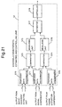
- Fig. 21 shows a configuration of another channel characteristic estimating and controlling unit according to the present embodiment.
- the other elements of the demodulator without shown in Fig. 21 is the same as the elements of the eighth embodiment shown in Fig. 19 or Fig. 20.
- reference numerals 570, 571 and 572 are temporary data discriminators, 573 and 574 are comparators, 575 and 576 show measuring units, 577 shows an estimator, and 578 shows a controller.
- the temporary data discriminator 570 temporarily discriminates the output from the quasi-coherent detecting unit 40
- the temporary data discriminator 571 temporarily discriminates the output from the signal compensator
- the temporary data discriminator 572 temporarily discriminates the output from the fading distortion compensator 52.
- the comparator 573 compares the outputs from the temporary data discriminators 570 and 571 and the comparator 573 outputs the comparison result.
- the comparator 574 compares the outputs from the temporary data discriminators 571 and 572 and the comparator 574 outputs the comparison result.
- the measuring unit 575 measures the comparison result supplied from the comparator 573
- the measuring unit 576 measures the comparison result supplied from the comparator 574.
- the estimator 577 estimates the channel condition, which varies, using the measured result of the measuring units 575 and 576.
- the controller 578 determines the weighted coefficient of the fading distortion estimator or tap coefficient of the averaging unit based on the channel condition estimated by the estimator 577, and parameters of the coefficient are respectively set.
- the demodulator of the ninth embodiment based on the demodulated data, which was compensated and output by the signal compensator, the data before fading distortion compensation and the data after fading distortion compensation are compared, the comparison result is measured, and the channel condition is estimated.
- the fading distortion can be estimated using the amount of characteristic improvement by the fading distortion compensation, and C/N can be also estimated using the amount of characteristic improvement by the averaging process.
- the parameters suitable to the channel condition can be set, and the demodulator having the most suitable receiving performance to the channel including wide range of characteristic from the fading channel to the nonfading channel.
- the signal is processed averaging to detect the estimation error caused by the thermal noise.
- the obtained estimation error is compounded to the estimated value supplied from the fading distortion estimator to obtain the reference signal to compensate the received signal.
- the estimation error caused by the thermal noise which was not sufficiently compensated conventionally by the fading distortion compensator, can be detected and the degradation of the characteristic caused by the fading and the thermal noise can be reduced.
- the demodulator of the invention first compensates the fading distortion using the known signal, and then averages the signal to detect the estimation error caused by the thermal noise, and the signal is compensated.
- the demodulator can detect the estimation error caused by the thermal noise and can reduce the degradation of the characteristics caused by the fading and the thermal noise by a simpler configuration.
- the demodulator of the invention averages the estimated value of the fading distortion obtained by the known signal block by adding the weighted value to the previous and subsequent signal blocks of the known signal block.
- the demodulator can reduce the degradation of the characteristic caused by the thermal noise with adapting the fading variation.
- the modulation component is eliminated by remodulating the signal using the output from the temporary data discriminator. Since the demodulator of the present invention can eliminate the modulation component more precisely than Nth power law and so on, which reduces the estimation error generated by the averaging unit. Further, the number of stages required for averaging can be decreased, thus the load of the averaging unit can be lessened.
- the modulation component is eliminated by re-modulating the signal using the output from the temporary data discriminator, which enables the demodulator of the present invention to eliminate the modulation component more precisely. Therefore, the estimation error generated by the averaging unit can be reduced. Further, the number of stages required for averaging can be decreased, thus the load of the averaging unit can be lessened.
- the demodulator of the present invention averages the signal, of which the modulation component was eliminated, by multiplying tap coefficients.
- the averaging can be processed according to the channel condition, which improves the performance of the receiver.
- the reliability factor is weighted to the data, which was processed by the hard data decision by the data discriminator, using the fading distortion information supplied from the fading distortion estimator.
- the Viterbi decoding is implemented by soil decision data according to the reliability factor, so that the error correction ability is improved, and the performance of the receiver has been improved.
- the channel condition is always estimated in order to set the most suitable control signal to the condition, which enables the subsequent coherent detection can be performed based on the characteristic variation of the channel. Therefore, the most suitable receiving performance can be obtained on receiving the signal from the fading channel to the nonfading channel.
Landscapes
- Engineering & Computer Science (AREA)
- Computer Networks & Wireless Communication (AREA)
- Signal Processing (AREA)
- Digital Transmission Methods That Use Modulated Carrier Waves (AREA)
- Mobile Radio Communication Systems (AREA)
- Noise Elimination (AREA)
Applications Claiming Priority (2)
| Application Number | Priority Date | Filing Date | Title |
|---|---|---|---|
| JP02055598A JP3475066B2 (ja) | 1998-02-02 | 1998-02-02 | 復調装置 |
| JP2055598 | 1998-02-02 |
Publications (3)
| Publication Number | Publication Date |
|---|---|
| EP0933902A2 true EP0933902A2 (fr) | 1999-08-04 |
| EP0933902A3 EP0933902A3 (fr) | 2002-09-18 |
| EP0933902B1 EP0933902B1 (fr) | 2004-04-07 |
Family
ID=12030415
Family Applications (1)
| Application Number | Title | Priority Date | Filing Date |
|---|---|---|---|
| EP99300466A Expired - Lifetime EP0933902B1 (fr) | 1998-02-02 | 1999-01-22 | Démodulation avec compensation d'évanouissements |
Country Status (3)
| Country | Link |
|---|---|
| US (1) | US6452983B1 (fr) |
| EP (1) | EP0933902B1 (fr) |
| JP (1) | JP3475066B2 (fr) |
Families Citing this family (15)
| Publication number | Priority date | Publication date | Assignee | Title |
|---|---|---|---|---|
| JP3289676B2 (ja) | 1998-05-28 | 2002-06-10 | 日本電気株式会社 | パイロット信号を含む受信信号の復調方法及びその装置 |
| WO2000076165A1 (fr) * | 1999-06-09 | 2000-12-14 | Mitsubishi Denki Kabushiki Kaisha | Controleur de frequences automatique |
| JP3581294B2 (ja) * | 2000-03-31 | 2004-10-27 | 株式会社東芝 | 受信装置 |
| JP2001339328A (ja) * | 2000-05-25 | 2001-12-07 | Communication Research Laboratory | 受信装置、受信方法、ならびに、情報記録媒体 |
| CN1393066A (zh) * | 2000-07-24 | 2003-01-22 | 三菱电机株式会社 | 无线通信接收装置及接收方法 |
| US20020172166A1 (en) * | 2001-03-22 | 2002-11-21 | Huseyin Arslan | Communications system and method for measuring short-term and long-term channel characteristics |
| JP3676986B2 (ja) | 2001-03-29 | 2005-07-27 | 松下電器産業株式会社 | 無線受信装置及び無線受信方法 |
| US7130587B2 (en) * | 2001-08-22 | 2006-10-31 | National Institute of Information and Communications Technology Incorporated, Administrative Agency | Communication quality estimation method, communication quality estimation apparatus, and communication system |
| KR100450949B1 (ko) * | 2001-09-18 | 2004-10-02 | 삼성전자주식회사 | 데이터 통신 시스템에서 채널 복호기 입력 연성 결정 값계산 장치 및 방법 |
| US7248625B2 (en) * | 2002-09-05 | 2007-07-24 | Silicon Storage Technology, Inc. | Compensation of I-Q imbalance in digital transceivers |
| US6885323B2 (en) * | 2003-06-27 | 2005-04-26 | Optichron, Inc. | Analog to digital converter with distortion correction |
| KR20050027785A (ko) * | 2003-09-16 | 2005-03-21 | 삼성전자주식회사 | 신호 품질 검출 방법 및 그 장치와, 이를 구현하기 위한프로그램이 기록된 기록매체 |
| US7979032B2 (en) * | 2007-12-18 | 2011-07-12 | Intel Corporation | Estimating statistical properties of noise in modulated data carrier signals |
| US8335438B2 (en) * | 2009-10-30 | 2012-12-18 | Fujitsu Limited | Estimating frequency offset using a feedback loop |
| US9203576B2 (en) | 2012-08-03 | 2015-12-01 | Telefonaktiebolaget L M Ericsson (Publ) | Quasi co-located antenna ports for channel estimation |
Family Cites Families (10)
| Publication number | Priority date | Publication date | Assignee | Title |
|---|---|---|---|---|
| JPH061908B2 (ja) * | 1988-02-02 | 1994-01-05 | 郵政省通信総合研究所長 | 伝送路歪補償方式 |
| US5400366A (en) * | 1992-07-09 | 1995-03-21 | Fujitsu Limited | Quasi-synchronous detection and demodulation circuit and frequency discriminator used for the same |
| KR100255726B1 (ko) * | 1993-03-31 | 2000-05-01 | 윤종용 | 자동 주파수 제어방법 및 장치 |
| JP3153869B2 (ja) * | 1993-05-11 | 2001-04-09 | 株式会社日立国際電気 | フェージング歪補償方式及びその回路 |
| EP0716520B1 (fr) * | 1994-06-23 | 2004-05-12 | NTT DoCoMo, Inc. | Circuit de demodulation de type cdma et procede de demodulation associe |
| DE69618200T2 (de) * | 1995-07-07 | 2002-06-20 | Nortel Networks Ltd., St.Laurent | Trägerrückgewinnung für digital phasenmodulierte signale, mittels einer phasemmodulierte bekannten folge |
| JP3013763B2 (ja) * | 1995-08-25 | 2000-02-28 | 日本電気株式会社 | キャリア同期ユニット |
| JPH09102806A (ja) * | 1995-10-06 | 1997-04-15 | Hitachi Denshi Ltd | 復調器 |
| JP3512296B2 (ja) * | 1996-03-08 | 2004-03-29 | 富士通株式会社 | フェージング等化器 |
| JP3327152B2 (ja) * | 1996-12-25 | 2002-09-24 | 三菱電機株式会社 | 自動周波数制御回路 |
-
1998
- 1998-02-02 JP JP02055598A patent/JP3475066B2/ja not_active Expired - Fee Related
-
1999
- 1999-01-22 EP EP99300466A patent/EP0933902B1/fr not_active Expired - Lifetime
- 1999-02-01 US US09/240,579 patent/US6452983B1/en not_active Expired - Fee Related
Also Published As
| Publication number | Publication date |
|---|---|
| EP0933902A3 (fr) | 2002-09-18 |
| US6452983B1 (en) | 2002-09-17 |
| EP0933902B1 (fr) | 2004-04-07 |
| JPH11220503A (ja) | 1999-08-10 |
| JP3475066B2 (ja) | 2003-12-08 |
Similar Documents
| Publication | Publication Date | Title |
|---|---|---|
| KR100505694B1 (ko) | 직접 계산 방식에 의한 코드화 직교 주파수 분할 다중화수신기의 채널 상태 평가 장치 및 그 방법 | |
| CN108234376B (zh) | 无线数据通信方法及装置 | |
| US6650718B1 (en) | Timing reproducer and demodulator comprising this | |
| US6243423B1 (en) | Receiver, transmitter-receiver, and communication method | |
| EP0933902B1 (fr) | Démodulation avec compensation d'évanouissements | |
| EP0736986B1 (fr) | Appareil de transmission et méthode associée, qui utilisent des données de référence, insérées dans le signal de transmission, pour estimer la qualité du canal de transmission | |
| US7477707B2 (en) | Computationally efficient demodulation for differential phase shift keying | |
| EP1453261B1 (fr) | Procédé d'estimation de canal pour un système de communication mobile | |
| US7940861B2 (en) | QAM phase error detector | |
| US6748026B1 (en) | Distortion estimation apparatus, frequency offset compensation apparatus and reception apparatus | |
| WO2002032067A1 (fr) | Procede de regulation de frequence automatique | |
| EP0692895A2 (fr) | Démodulateur utilisant une détection différentielle | |
| US6442218B1 (en) | Demodulator | |
| US20040252788A1 (en) | Demodulation for phase modulation | |
| JP2008530951A (ja) | 予め符号化された部分応答信号用の復調器および受信器 | |
| EP1245103B1 (fr) | Correction du decalage dans un systeme de communication a etalement du spectre | |
| EP0851640B1 (fr) | Correction de décalages du composant continu et de phase, dans des récepteurs de signaux MDP | |
| US6965654B1 (en) | Frequency offset quantity detecting apparatus | |
| US7583741B2 (en) | Likelihood corrector and likelihood correction method | |
| JP3018840B2 (ja) | フェージング補償装置 | |
| JP7660970B2 (ja) | 対数尤度比算出回路および無線受信装置 | |
| EP1313279A1 (fr) | Procédé de correction de décalages de phase dans un signal et récepteur correspondant | |
| KR100592704B1 (ko) | 무선 디지털 통신시스템에서 주파수 및 위상 옵셋의 동시추정 방법 | |
| EP2068521B1 (fr) | Détecteur d'erreur de phase QAM | |
| JP4435005B2 (ja) | 等化器 |
Legal Events
| Date | Code | Title | Description |
|---|---|---|---|
| PUAI | Public reference made under article 153(3) epc to a published international application that has entered the european phase |
Free format text: ORIGINAL CODE: 0009012 |
|
| AK | Designated contracting states |
Kind code of ref document: A2 Designated state(s): AT BE CH CY DE DK ES FI FR GB GR IE IT LI LU MC NL PT SE |
|
| AX | Request for extension of the european patent |
Free format text: AL;LT;LV;MK;RO;SI |
|
| PUAL | Search report despatched |
Free format text: ORIGINAL CODE: 0009013 |
|
| AK | Designated contracting states |
Kind code of ref document: A3 Designated state(s): AT BE CH CY DE DK ES FI FR GB GR IE IT LI LU MC NL PT SE |
|
| AX | Request for extension of the european patent |
Free format text: AL;LT;LV;MK;RO;SI |
|
| 17P | Request for examination filed |
Effective date: 20020906 |
|
| 17Q | First examination report despatched |
Effective date: 20021206 |
|
| GRAH | Despatch of communication of intention to grant a patent |
Free format text: ORIGINAL CODE: EPIDOS IGRA |
|
| AKX | Designation fees paid |
Designated state(s): FR GB IT |
|
| REG | Reference to a national code |
Ref country code: DE Ref legal event code: 8566 |
|
| GRAS | Grant fee paid |
Free format text: ORIGINAL CODE: EPIDOSNIGR3 |
|
| GRAA | (expected) grant |
Free format text: ORIGINAL CODE: 0009210 |
|
| AK | Designated contracting states |
Kind code of ref document: B1 Designated state(s): FR GB IT |
|
| REG | Reference to a national code |
Ref country code: GB Ref legal event code: FG4D |
|
| PLBE | No opposition filed within time limit |
Free format text: ORIGINAL CODE: 0009261 |
|
| STAA | Information on the status of an ep patent application or granted ep patent |
Free format text: STATUS: NO OPPOSITION FILED WITHIN TIME LIMIT |
|
| PG25 | Lapsed in a contracting state [announced via postgrant information from national office to epo] |
Ref country code: FR Free format text: LAPSE BECAUSE OF FAILURE TO SUBMIT A TRANSLATION OF THE DESCRIPTION OR TO PAY THE FEE WITHIN THE PRESCRIBED TIME-LIMIT Effective date: 20050311 |
|
| EN | Fr: translation not filed | ||
| 26N | No opposition filed |
Effective date: 20050110 |
|
| REG | Reference to a national code |
Ref country code: FR Ref legal event code: RN Ref country code: FR Ref legal event code: FC |
|
| ET | Fr: translation filed | ||
| PGFP | Annual fee paid to national office [announced via postgrant information from national office to epo] |
Ref country code: IT Payment date: 20060131 Year of fee payment: 8 |
|
| PGFP | Annual fee paid to national office [announced via postgrant information from national office to epo] |
Ref country code: GB Payment date: 20070117 Year of fee payment: 9 |
|
| PGFP | Annual fee paid to national office [announced via postgrant information from national office to epo] |
Ref country code: FR Payment date: 20070109 Year of fee payment: 9 |
|
| GBPC | Gb: european patent ceased through non-payment of renewal fee |
Effective date: 20080122 |
|
| REG | Reference to a national code |
Ref country code: FR Ref legal event code: ST Effective date: 20081029 |
|
| PG25 | Lapsed in a contracting state [announced via postgrant information from national office to epo] |
Ref country code: GB Free format text: LAPSE BECAUSE OF NON-PAYMENT OF DUE FEES Effective date: 20080122 |
|
| PG25 | Lapsed in a contracting state [announced via postgrant information from national office to epo] |
Ref country code: IT Free format text: LAPSE BECAUSE OF NON-PAYMENT OF DUE FEES Effective date: 20070122 |
|
| PG25 | Lapsed in a contracting state [announced via postgrant information from national office to epo] |
Ref country code: FR Free format text: LAPSE BECAUSE OF FAILURE TO SUBMIT A TRANSLATION OF THE DESCRIPTION OR TO PAY THE FEE WITHIN THE PRESCRIBED TIME-LIMIT Effective date: 20080131 |